EP2109223A2 - Analog-Digital-Umwandlung bei Pixelarrays - Google Patents
Analog-Digital-Umwandlung bei Pixelarrays Download PDFInfo
- Publication number
- EP2109223A2 EP2109223A2 EP09153222A EP09153222A EP2109223A2 EP 2109223 A2 EP2109223 A2 EP 2109223A2 EP 09153222 A EP09153222 A EP 09153222A EP 09153222 A EP09153222 A EP 09153222A EP 2109223 A2 EP2109223 A2 EP 2109223A2
- Authority
- EP
- European Patent Office
- Prior art keywords
- analog
- signal
- counter
- ramp signal
- level
- Prior art date
- Legal status (The legal status is an assumption and is not a legal conclusion. Google has not performed a legal analysis and makes no representation as to the accuracy of the status listed.)
- Granted
Links
Images


Classifications
-
- H—ELECTRICITY
- H03—ELECTRONIC CIRCUITRY
- H03M—CODING; DECODING; CODE CONVERSION IN GENERAL
- H03M1/00—Analogue/digital conversion; Digital/analogue conversion
- H03M1/10—Calibration or testing
- H03M1/1009—Calibration
- H03M1/1014—Calibration at one point of the transfer characteristic, i.e. by adjusting a single reference value, e.g. bias or gain error
- H03M1/1019—Calibration at one point of the transfer characteristic, i.e. by adjusting a single reference value, e.g. bias or gain error by storing a corrected or correction value in a digital look-up table
-
- H—ELECTRICITY
- H04—ELECTRIC COMMUNICATION TECHNIQUE
- H04N—PICTORIAL COMMUNICATION, e.g. TELEVISION
- H04N25/00—Circuitry of solid-state image sensors [SSIS]; Control thereof
- H04N25/60—Noise processing, e.g. detecting, correcting, reducing or removing noise
- H04N25/616—Noise processing, e.g. detecting, correcting, reducing or removing noise involving a correlated sampling function, e.g. correlated double sampling [CDS] or triple sampling
-
- H—ELECTRICITY
- H04—ELECTRIC COMMUNICATION TECHNIQUE
- H04N—PICTORIAL COMMUNICATION, e.g. TELEVISION
- H04N25/00—Circuitry of solid-state image sensors [SSIS]; Control thereof
- H04N25/70—SSIS architectures; Circuits associated therewith
- H04N25/76—Addressed sensors, e.g. MOS or CMOS sensors
- H04N25/78—Readout circuits for addressed sensors, e.g. output amplifiers or A/D converters
-
- H—ELECTRICITY
- H03—ELECTRONIC CIRCUITRY
- H03M—CODING; DECODING; CODE CONVERSION IN GENERAL
- H03M1/00—Analogue/digital conversion; Digital/analogue conversion
- H03M1/12—Analogue/digital converters
- H03M1/1205—Multiplexed conversion systems
- H03M1/123—Simultaneous, i.e. using one converter per channel but with common control or reference circuits for multiple converters
-
- H—ELECTRICITY
- H03—ELECTRONIC CIRCUITRY
- H03M—CODING; DECODING; CODE CONVERSION IN GENERAL
- H03M1/00—Analogue/digital conversion; Digital/analogue conversion
- H03M1/12—Analogue/digital converters
- H03M1/124—Sampling or signal conditioning arrangements specially adapted for A/D converters
- H03M1/129—Means for adapting the input signal to the range the converter can handle, e.g. limiting, pre-scaling ; Out-of-range indication
- H03M1/1295—Clamping, i.e. adjusting the DC level of the input signal to a predetermined value
-
- H—ELECTRICITY
- H03—ELECTRONIC CIRCUITRY
- H03M—CODING; DECODING; CODE CONVERSION IN GENERAL
- H03M1/00—Analogue/digital conversion; Digital/analogue conversion
- H03M1/12—Analogue/digital converters
- H03M1/20—Increasing resolution using an n bit system to obtain n + m bits
- H03M1/202—Increasing resolution using an n bit system to obtain n + m bits by interpolation
- H03M1/203—Increasing resolution using an n bit system to obtain n + m bits by interpolation using an analogue interpolation circuit
-
- H—ELECTRICITY
- H03—ELECTRONIC CIRCUITRY
- H03M—CODING; DECODING; CODE CONVERSION IN GENERAL
- H03M1/00—Analogue/digital conversion; Digital/analogue conversion
- H03M1/12—Analogue/digital converters
- H03M1/50—Analogue/digital converters with intermediate conversion to time interval
- H03M1/56—Input signal compared with linear ramp
Definitions
- This invention relates to analog-to-digital conversion which can be used, for example, in processing signals output from a pixel array.
- Imaging sensors comprise an array of unit elements (pixels).
- the array of pixels is exposed to radiation during an exposure period and, subsequently, the signal value of each pixel is read from the array.
- the array can be a one dimensional array (linear sensor) or a two dimensional array (area array) with pixels arranged in rows and columns.
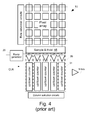
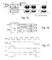
- Figure 1 shows the architecture of a CMOS imaging sensor. Impinging photons are converted into charges in the pixel array and are accumulated during a certain integration period. Typically, the pixels are selected row by row for readout of their signals.
- a typical 4T pixel is shown in Figure 2 .
- the pixel includes a photodiode PD, a transfer gate to transfer the charges in the photodiode to the floating diffusion FD, a reset transistor M1, a source follower M2 and a row selection transistor M3.
- the reset transistor is used to reset the floating diffusion FD to a known state before transferring charge from the photodiode PD to it as is known in the art.
- the source follower M2 converts the charges stored at the floating diffusion FD into an electrical output voltage signal at the column bus.
- the useful signal outputs of a pixel are analog voltages representing: (i) the reset signal level V reset and (ii) the signal level V sig that is generated after charge transfer from the photodiode.
- the final signal that represents the amount of photons impinged onto the pixel is the difference signal between these two signals.
- the two signals, or the difference between these signals, must be converted from an analog value to a digital value.
- the analog-to-digital conversion is performed by a single ADC 16 in the output stage of the array and this single ADC 16 is used, on a time-shared basis, by the column circuits.
- signal values are transferred from each of the column circuits to the ADC 16 and converted to digital form.
- FIG. 3 shows an alternative approach. Analog-to-digital conversion is performed, in parallel, in each column of the array.
- the single-slope ADC comprises a ramp generator 20 and a synchronous counter 17.
- Each column has data latches 18 and a comparator 19.
- a ramp signal is applied to each of the columns circuits. The ramp signal is distributed to all columns.
- the counter 17 is incremented in synchronism with the ramp signal such that, at any point in time, the counter 17 provides a digital representation of the analog value of the ramp signal output by the ramp generator 20.
- the comparator 19 in each column compares the level of the input signal (V reset or V sig ) against the gradually changing ramp signal.
- the comparator 19 output changes state and latches the digital code of the counter into a first memory 18. Afterwards, the same process is repeated for the other of the signals (V reset , V sig ) and the code is latched into a second memory. The difference in digital codes is then sent to the output of the sensor.
- TDI Time Delay and Integration
- US 7,129,509 describes an imaging system for performing TDI in which an output signal from a column of a pixel array is first converted to digital form and then added to a value which has been stored in digital memory. Although accumulation in the digital domain can have some advantages, the technique described in US 7,129,509 requires a separate storage register and adder to perform the addition of the digital value representing the latest exposure level of an element of the pixel array, with a previously stored value. This can be expensive in terms of area and layout in a semiconductor device.
- the rate at which the ADC can operate is limited by several constraints.
- a significant constraint is the period of the ramp signal against which the analog reset level and signal level are compared.
- the gradient of the ramp signal V ramp signal can be increased but, for a given resolution (number of bits), it is necessary to proportionally increase the frequency of the master clock that is distributed to the counters in the column processing units. In practice, there is a limit to the clock frequency that can be achieved.
- the present invention seeks to provide an alternative way of performing analog-to-digital conversion.
- a first aspect of the present invention provides an analog-to-digital converter for generating an output digital value equivalent to the difference between two analog signal values comprising:
- This aspect of the invention can have an advantage of avoiding the need to distribute a counter signal across multiple ADC units, which improves the accuracy of the accumulated value. It can also avoid the need for counter direction changing circuitry as each counter is only required to count in a single direction.
- the analog-to-digital converter performs the conversion during a conversion cycle.
- the conversion cycle can make use of a ramp signal having two cycles, or just a single cycle.
- the use of a single ramp cycle can reduce the conversion time as both of the analog signals are compared with the same cycle of the ramp signal.
- the comparison of the first and second analog signals with the ramp signal can occur concurrently or sequentially during the ramp signal.
- the control stage can use an intentional offset during the comparisons of the first and second analog signals with the ramp signal.
- the value accumulated by the counter can be output directly, or the analog-to-digital converter can comprise an inversion function for inverting the value of the counter.
- control stage is arranged to enable counter circuitry based on a comparison of the analog ramp signal with the first analog signal and the second analog signal, and the counter circuitry comprises:
- the comparison of the ramp signal with the first analog signal and the second analog signal produces a pulsed signal which is asynchronous with respect to the clock signal and wherein:
- control stage is arranged to translate the period between an edge of the pulsed signal and a predetermined point which is synchronous with the clock signal into a longer period which is measurable by the second counter using the clock signal.
- a further aspect of the invention provides an analog-to-digital conversion apparatus comprising: a plurality of the analog-to-digital converters arranged in parallel; and a signal generator for generating the ramp signal, wherein the signal generator provides the ramp signal input to each of the plurality of converters.
- the analog-to-digital conversion apparatus comprises a storage element for the first analog signal level and a storage element for the second analog signal level.
- a second aspect of the present invention provides a processing unit for a pixel array, the processing unit being arranged to accumulate digital signal values for elements of an image over multiple exposure periods and comprising an analog-to-digital converter (ADC) for generating an output digital value equivalent to an analog signal value derived from a pixel of the pixel array, wherein the analog-to-digital converter comprises:
- This aspect of the invention is particularly advantageous in Time Delay and Integration (TDI) applications and any application where multiple values need to be accumulated.
- TDI Time Delay and Integration
- a counter can be allocated to accumulate the digital signal value for a particular element of the image across the multiple exposure periods.
- an ADC can be associated with a pixel, or line of pixels, of the pixel array with an accumulated digital value being held in a memory and loaded into the counter as the starting digital value at the start of a processing operation for each exposure period.
- the processing unit monitors the accumulated digital value and determines if any further processing operations should occur. This determination can be based on the current accumulated exposure level. Operating in this manner makes it possible to prevent saturation of image elements, before saturation occurs. The determination can be made independently for each accumulated element of the image.
- control stage causes the number of exposure periods for which accumulation has occurred to be stored in the memory.
- a third aspect of the present invention provides a processing unit for a pixel array, the processing unit comprising an analog-to-digital converter for generating an output digital value equivalent to an analog signal value derived from a pixel of the pixel array, wherein the analog-to-digital converter comprises:
- This aspect of the invention can have an advantage of increasing speed of conversion in the ADC without requiring a high speed clock signal.
- each of the aspects of the invention is applied to the processing of analog output signals from a pixel array.
- the analog-to-digital converter can be used to process an output of a pixel or a group of pixels (e.g. a column) of the pixel array.
- the analog signal levels can correspond to a reset level of a pixel and a signal value of the pixel following exposure to radiation.
- a plurality of the analog-to-digital converters are arranged in parallel.
- Each analog-to-digital converter receives the same ramp signal as an input.
- Each ADC is associated with a pixel (e.g. linear 1D array) or a line of pixels of the pixel array.
- the analog-to-digital converter, or parallel set of ADCs is advantageously provided on the same semiconductor device (e.g. integrated circuit) as a pixel array, although the analog-to-digital converter, or set of ADCs, can be provided on a separate semiconductor device.
- the analog-to-digital converter can be also used in a 3D integrated sensor.
- a 3D integrated sensor is a sensor that is built up from multiple chips that are stacked on top of each other. For example, a first chip contains the pixel photodiodes or pixel circuitry. This chip is bonded to a second chip containing readout circuitry (e.g. analog processing circuits or ADCs) and so on.
- the invention also provides a corresponding method for each of the aspects of the invention.
- first, second and third aspects of the present invention can be combined with one another.
- the first aspect of the invention can make use of the features of the third aspect of the invention to improve conversion speed.
- FIG. 6 shows an architecture of a sensor which includes column processing stages to perform double sampling, or correlated double sampling (CDS), in accordance with an embodiment of the present invention
- Figures 7 and 8 show two alternative ways in which the column processing stages 30 of Figure 6 can operate.
- Each of the parallel set of column processing stages 30 comprises a comparator 19 and a unidirectional counter 32.
- the use of a unidirectional counter avoids the need for any circuitry to change the direction of counting.
- a ramp generator 20 generates a ramp signal which is distributed to each column processing stage 30.
- a clock signal CLK is also distributed to each column processing stage 30.
- Comparator 19 receives the ramp signal on one of the comparator inputs.
- Each of the signals (V reset , V sig ) held by the sample and hold circuitry 15 is sequentially applied to the other comparator input.
- the comparator 19 enables counter 32 based on the comparison of the input signals (V reset , V sig ) with the ramp signal.
- counter 32 holds a count value which is representative of the difference between the two analog signals (V reset , V sig ).
- Column selection circuits 33 selectively transfer, on a time-shared basis, the digital values held by counters 32 to the output 34.
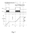
- the first operating scheme is shown in Figure 7 .
- the reset level V reset is compared with the ramp signal.
- the ramp signal begins at time t1.
- the counter begins at time t2 when the ramp signal equals the reset level V reset and the counter is stopped at time t3 at the end of the ramp.
- the signal level V sig is compared with the ramp signal.
- the ramp signal begins at time t4.
- the counter is also restarted at the same time, t4, and continues to count in the same direction from the value accumulated at time t3.
- the counter is stopped at time t5 when the ramp signal equals the signal level V sig .
- the ramp signal ends at time t6.
- the second operating scheme is shown in Figure 8 and this is essentially an inverse of the operation shown in Figure 7 .
- the reset level V reset is compared with the ramp signal.
- the ramp signal begins at time t1 and the counter also begins at t1.
- the counter is stopped.
- the ramp signal ends at time t3.
- the signal level V sig is compared with the ramp signal.
- the ramp signal begins at time t4.
- time t5 when the ramp signal equals the signal level V sig , the counter is restarted, and continues to count in the same direction from the value accumulated at time t2.
- the ramp signal ends and the counter is stopped.
- the final counter value corresponds in this case to the 'inverse' signal (counter value is maximum for small signals).
- the ramp signal has a smaller amplitude range, and a shorter period, in the first phase of the operating cycle compared to the second phase of the operating cycle. This is possible because the range of reset levels (including pixel, column and comparator offsets and noise) is considerably smaller than the range of the signal representing an exposure level of a pixel. Providing a ramp signal with two different ranges and/or periods, helps to reduce the overall length of the conversion cycle.
- the double sampling operation requires two separate phases of a conversion cycle, with the ramp signal being reset between the two phases.
- the reset level V reset is compared with the ramp signal
- the signal level V sig is compared with the ramp signal.
- the conversion cycle has a single phase with a single ramp signal and both the reset level V reset and the signal V sig are compared with the same ramp signal.
- the two signals to be converted are made available concurrently, e.g. by sample and hold circuitry 15 at the output of the column.
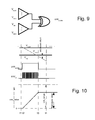
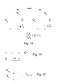
- the first technique shown in Figures 9 and 10 , uses comparison logic which is capable of comparing both the reset level V reset and the signal V sig with the ramp signal.
- the comparison logic can comprise a comparator with three inputs or, as shown in Figure 9 , it can comprise two comparators each having two inputs and an exclusive OR gate.
- the ramp signal starts at time t1 and ends at time t4. When the ramp signal equals the reset level V reset , at time t2, the counter is enabled and stays enabled until the ramp signal equals the signal level V sig , at time t3.
- the comparison is not an exact comparison of the levels, but includes a systematic offset of at least 1 clock period for the case that the signal level equals the reset level (i.e. for net zero input, the enable signal for the counter is at least 1 clock period long).
- This is advantageous to ensure that all random variations of the comparators (in the columns) can be measured, i.e. the systematic offset is larger than the largest possible random offset such that the counter value is larger than zero for net zero input.
- the systematic offset can also be ensured by using an offset in the V ramp generation of one of the comparators.
- These systematic offsets (and random variation of this systematic offset) can then be calibrated and stored periodically (e.g. each frame or at start up of the sensor) by setting signal equal to reset signal and storing the result which is then systematically subtracted from each measurement (could be only a few bits, subtraction at output or during initialization of the counters).
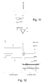
- the second technique is schematically depicted in Figures 11 and 12 .
- Sample & hold capacitors C R (x), C S (x) store the reset level and the signal level of a pixel in the pixel array.
- a single comparator 40 is used within the column processing stage 30.
- a first input 41 of comparator 40 receives the ramp signal and the second input 42 of comparator 40 receives one of the sampled signals held on capacitors C R (x), C S (x).
- comparator input 42 is connected to the first capacitor C R (x) that is storing the reset level. Once the ramp signal reaches the reset level, the comparator input 42 is disconnected from this first capacitor C R (x), and connected to the second capacitor C S (x) which is storing the signal level including an offset.
- an intentional offset is used on the reference signal. This helps to ensure that all random variations in case of small signals are converted.
- the intentional offset is required because switching the input from V reset to V sig takes some time (while the ramp signal is continuously changing).
- the stored values can be subtracted on-chip (e.g. at the output or by proper initialization of the counters) or off-chip.
- the calibration does not need to be performed each row, but can be performed only from time to time.
- Time Delay and Integration Imaging process
- TDI Time Delay Integration
- line scan applications where the light level is low, or where the relative speed of the movement is large
- Time Delay Integration (TDI) image sensors are useful.
- the pixel signals delivered by the pixels of the same column are in that case adequately delayed and added synchronously with the optical scanning.
- the light from a given point in the scene impinges successively on each pixel of the given corresponding column.
- the signals from each of the rows are added to increase the final SNR.
- a simple example of the TDI principle is illustrated in Figure 13 .
- a 1D image sensor comprising a column of pixels (Pixel 1, pixel 2, pixel 3) 120 is shown.
- a subject 122 is moved past the image sensor 120 in the direction 121.
- Five separate integration periods are shown.
- the first integration period the first element of subject 122 is detected by pixel 1 of the sensor 120 and stored in a first storage device of processing circuitry 124, which can be located on or off-chip.
- the first element of subject 122 is detected by pixel 2 of the sensor 120 and is summed (integrated) with the previously stored copy of the same element in the first storage device of processing circuitry 124 (which now shows a count of "2").
- the second element of subject 122 is detected by pixel 2 of the sensor 120 and is stored in a second storage device of processing circuitry 124. The process continues over subsequent integration periods, with each storage device in processing circuitry 124 accumulating multiple detected copies of the same elements of subject 122.
- a first scheme uses a single counter in combination with a memory array (e.g. DRAM like).
- Figure 14 shows the image sensor of Figure 6 with additional apparatus to perform TDI.
- the image sensor comprises a pixel array 10 with an output per column.
- Sample & hold stages 15 are not always required, depending on the readout timing.
- Each column has a column processing unit 30 which includes a comparator and a counter 32.
- Each column processing unit 30 is associated with a set of storage locations 51 which are accessible by the column processing unit 30.
- a bus connects the column processing unit 30 to the storage locations 51.
- a read/write control signal 53 controls direction of flow of data between a storage location 51 and a counter 32, and a switch 52 at each storage location determines which storage location is used to store a counter value, or determines from which storage location an accumulated value is read.
- the counter 32 in a column processing unit 30 is initialised with an accumulated signal value stored in a memory location. Counter 32 then begins to count in the manner described in any of Figures 5 , 7 or 8 , with the difference that the count begins at the value loaded from the storage location (and representing the accumulated value over previous TDI integration cycles). The counter 32 is incremented according to the reset and signal values (V reset , V sig ) for the currently selected pixel.
- the counter value is written to the appropriate memory location.
- the memory is read out in a rolling readout sequence (readout pointer required).
- the last memory location (holding the fully accumulated TDI signal) always has to be read out.
- a second scheme adds a new pixel signal to an already accumulated signal by choosing and incrementing the appropriate counter in the A/D conversion process.
- There is an array of counters and logic routes the new signal to the correct counter and the counters themselves act as memories in this case.
- a counter comprises a number of flip flops and is thus able to store the signal, as it behaves in a similar manner to static memory. The enable signal, clock signal and ramp signal are routed to the correct counter.
- This aspect of the invention can use a single direction counter with a single ramp cycle, or two ramp cycles. It can alternatively use a counter with up/down counting as described in US 7,088,279 .
- the dynamic range of a TDI pixel is practically unlimited if the bit depth of the counter is sufficient.
- the dynamic range of the TDI signal can be controlled as follows. This technique can be applied to TDI sensors as well as to linear sensors (or any other kind of sensor) where a pixel signal value is accumulated by reading a pixel multiple times during a frame period.
- the principle is illustrated in Figure 15 for a TDI sensor.
- the counter shown in Figure 15 can be the unidirectional counter 32 previously described.
- a memory location 51 stores an accumulated TDI signal.
- An additional counter 55 maintains a count of the number of TDI cycles that have been performed.
- An additional memory location 54 is associated with memory location 51.
- the additional memory location 54 stores a count of the number of TDI cycles (addition cycles) for which the signal value has been accumulated. After each addition a decision is made as to whether the next addition should take place or not. As an example, if the accumulated counter value stored in memory location 51 exceeds a certain (pre-defined or programmable) value (logic operation in the counter), the addition of the next pixel signal is suppressed and the TDI depth (i.e. the number of TDI cycles, or the number of addition steps up to that point) is memorised. A practical example will now be described. Consider that there are eight TDI cycles and that counter 32 is a 6-bit counter 32.
- Each TDI cycle contributes a signal which increases the counter value by '000011' (as an example). After eight such TDI cycles the final value of counter 32 will be about '011000', resulting from eight additions of approximately the same signal '000011'. The additional memory location 54 will, in this case, indicate '111 as eight TDI cycles were performed without reaching the maximum value of counter 32.
- a TDI imaging process of a relatively bright object Each TDI cycle contributes a signal which increases the counter value by '001011' (as an example). After four such TDI cycles the value of counter 32 is about '101100'.
- '100000' is taken as a threshold counter value, this means that any further addition operations are suppressed.
- the final value of counter 32 remains as '101100' and the additional memory location 54 contains a value '011', meaning that the value held in counter 32 was reached after 4 addition operations. If the TDI process had continued, the final counter value would have been '111111' with no indication of when this value was reached, i.e. a useless saturated signal.
- the TDI counter value in the second memory location 54 can be incremented at each addition step or, alternatively, the TDI counter value can be written into the second memory location 54 only when it is required. Memory access to memory location 51 is frozen for future additions. This means that each pixel of the final image can have its own optimal TDI level and at the same time use the full dynamic range offered by the accumulator.
- the final signal (expressed as bits/s) is equal to 'TDI value / T int ', where TDI value is the value accumulated and stored in memory, and T int is the total integration period.
- the signal for a particular image element is equal to: TDI value * / f ⁇ T int where TDI value* is the accumulated value stored in memory location 51 and f is the fraction of the total integration period, based on the value stored in memory location 54.
- This aspect of the invention can use a single direction counter with a single cycle, or two cycles. It can alternatively use a counter with up/down counting as described in US 7,088,279 .
- the rate at which the ADC can operate is limited by several constraints.
- a significant constraint is the period of the ramp signal (V ramp in Figure 7 ) against which the analog reset level and signal level are compared.
- the gradient of the ramp signal V ramp signal can be increased but, for a given resolution (number of bits), it is necessary to proportionally increase the frequency of the master clock that is distributed to the counters in the column processing units 30. In practice, there is a limit to the clock frequency.
- the conversion time: T conversion 2 N ⁇ T clock with N is the number of wanted bits and T clock is the master clock period.
- the master clock is used to derive only the M most significant bits and an additional mechanism is used to derive the remaining L least significant bits LSBs (with L equal or larger than N-M).
- the additional mechanism is a phase detection method which detects the phase shift between the clock signal and an ENABLE signal, indicating the start or stop of the counter.
- it is not essential to resolve the phase detection with absolute accuracy, good relative accuracy with good linearity is sufficient.
- the phase detection is resolved with a resolution of T clock /2 L with L an integer value, but it is not mandatory.
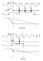
- Figure 16 schematically shows the overall apparatus and Figure 17 shows a timing diagram for the operation of the apparatus.
- a clock signal and an enable signal are applied to logic 60.
- the clock signal is the signal CLK shown in Figure 6 which is distributed to the parallel set of column processing units 30.
- the enable signal is generated by comparator 32 by comparing the ramp signal with the reset level and the signal level.
- the enable signal is asynchronous with respect to the clock, i.e. the start and end of the enable signal do not necessarily coincide with the cycles of the clock.
- the total period that the enable signal is high is represented by the combination of C MSB , C 1 and C 2 .
- Pulsed signals C MSB , C 1 and C 2 are generated by logic.
- the respective counters MSB counter, LSB counter 1, LSB counter 2 compute these respective parts of the overall time period.
- C MSB is synchronous with the main clock signal and indicates the number of complete clock cycles.
- C 1 and C 2 are pulses that are active high until the next rising edge of the clock signal following a rising/falling edge of the enable signal respectively.
- the main counter counts the number of master clock cycles which occur during this time period. In Figure 16 this is achieved by applying the clock signal and signal C MSB to an AND gate and outputting the resulting signal to the MSB counter.
- the clock signal and signal C 1 are applied to Interpolator 1, and the output of Interpolator 1 is applied to LSB counter 1.
- LSB counter 1 counts the fractions of a clock cycle which occur between the rising edge of the enable signal and the next rising edge of the clock signal.
- the clock signal and signal C 2 are applied to Interpolator 2, and the output of Interpolator 2 is applied to LSB counter 2.
- LSB counter 2 counts the fractions of a clock cycle which occur between the falling edge of the enable signal and the next rising edge of the clock signal.
- Length of ENABLE pulse DN MSB x T clock + (DN 1 - DN 2 ) x T clock /2 L
- L the number of equivalent bits (LSBs) of the interpolators.
- L is an integer value
- the signal is a simple concatenation of the values (e.g. if DN MSB is '0110' and DN 1 is '1010', then the final value is '01101010').
- Two interpolators are not always needed, such as when one of the edges of the enable signal is synchronous with the clock. It is possible to re-use the same interpolator to measure the C 2 pulse if the length of the enable signal is larger than the time the interpolator needs to convert the C 1 pulse. This is also possible when two ramp cycles are used for the analog-to-digital conversion operation. Three examples of implementation of the interpolation will now be described.
- the pulses C 1 and C 2 are less than one clock cycle in duration, with the pulses ending with a rising edge of the next clock cycle. It is also possible to make the pulses C 1 and C 2 , or at least one of these pulses, have a duration of at least one clock cycle. This can be useful to ensure that the value of the LSB counter is larger than zero, and serves a similar purpose as the intentional offset previously described.
- the rising edge of a clock cycle is used as an easily identifiable point of reference in Figure 17 , although it is possible to use any other identifiable feature of the clock cycle as an alternative to the rising edge.
- the example shown in Figure 17 has an ENABLE signal which results from comparing a ramp signal against two analog signal levels.
- each end of the ENABLE signal is asynchronous with respect to the clock and therefore both ends of the ENABLE signal need to be accurately measured.
- the ENABLE signal results from comparing a ramp signal against one analog signal level, such as an exposure level of a pixel, then the ENABLE signal can be arranged to start synchronously with the clock signal and it is only the end of the ENABLE signal which is asynchronous with respect to the clock signal. Thus, it is only necessary to accurately measure the end portion of the ENABLE signal.
- Figures 18-21 show a pulse stretching technique.
- Figure 18 shows an arrangement of two capacitors C A , C B used in the process.
- V A and V B are the respective voltages across the capacitors.
- Figure 19 shows logic used to generate the signal C' in Figure 18.
- Figure 20 shows a comparator which generates a stretched pulse C stretched in response to the voltages V A and V B .
- pulse C represents C 1 or C 2 shown in Figure 17 , i.e. a pulse generated at a start or end of the enable signal which it is desired to measure. Pulse C has a width which is less than T clock
- the pulse stretching technique measures the length of pulse C by forming a stretched pulse C stretched and measuring the length of the stretched pulse by counting the number of clock cycles.
- the enable signal goes high and pulse C also goes high.
- C' also goes high using the logic gate of Figure 19 .
- the switches shown in Figure 18 are closed and this starts the discharge of capacitors C A .and C B .
- the current sources I A and I B are connected to the respective capacitors.
- the comparator shown in Figure 20 compares voltages V A and V B and provides a high output as long as V B is above V A .
- the discharge of C A is stopped at the end of pulse C (time t2). Since V A has decreased faster than V B , signal C' remains high.
- pulse C stretched. has a length of three full clock cycles (after the C pulse) and if pulse C were equal to the length (T clock ) of a clock cycle, pulse C stretched would have a length of four clock cycles. Therefore, it is possible to deduce that C is at least three quarters of a clock cycle in length.
- pulse C stretched. has a length of more than one full clock cycle (after the C pulse) since pulse C has a length of more than one quarter of the clock period.
- Figures 18-21 show a simple way of performing the stretching, which should be easy to integrate with relatively good matching, but it will be appreciated that other techniques may exist.
- Figures 22 and 23 show another method to implement the interpolator.
- a pulse C is generated between the start or fall of the enable signal and the rising edge of the next clock cycle.
- This will be called an input pulse because, in this embodiment, the input pulse is circulated around a delay loop.
- the delay loop includes a pulse shrinking element which has the function of reducing the length of the pulse during each cycle around the delay loop. The reduction in length is a constant w.
- the pulse C begins at time t1 and ends at time t2.
- a pulse of length W-w original length minus constant w
- the length of the pulse is reduced by w after each cycle in the loop.
- the pulse appears for the last time and afterwards disappears completely.
- the pulse that is circulated around the loop is used as a clock input for a counter 61.
- the delay in the loop must be longer than the maximum width of the input pulse C. The technique is very easy to implement and consumes almost no power.
- T conversion T clock + f ⁇ T clock / W
- f the margin to make sure that the delay in the loop is larger than the maximal input width.
- the constant w should ideally be equal to T clock /2 L , however, it is not mandatory.
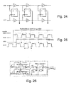
- Figure 24 shows two delay lines with a small (defined) difference in delay are used for time resolving.
- the start signal which corresponds to the rising edge of pulse C 1 or C 2 shown in Figure 17 is fed into a delay line with a propagation delay of T s .
- the stop signal is fed into a second delay line with a shorter propagation delay T f .
- the stop signal is synchronous with the master clock. Since the stop signal propagates faster, it will catch up with the start signal and the latched outputs of the flip-flops will be toggled from 0 to 1 from then on (thermometer code).
- the effective time resolution is the delay propagation difference (T s -T f ).
- Figure 25 shows the corresponding timing diagram.
- the oscillators could be voltage controlled oscillators (VCOs) which are controlled by reference phase-locked loops (PLLs) having a copy of the corresponding VCO, and deduced from a signal clock.
- VCOs voltage controlled oscillators
- PLLs reference phase-locked loops
- the delay lines could be controlled by DLL or in case of the Vernier based technique a dual DLL (course counting by master clock, fine counting by latching the status of the VCO or through Vernier line (from the paper " A High-Precision Time-to-Digital Converter Using a Two-Level Conversion Scheme", Hwang et al, IEEE Transcations on Nuclear Science, Vol.51, No.4, August 2004, pp.1349-1352 .)
- Figure 28 below shows how the delay lines can be controlled by a dual DLL.
- Both of the papers cited above (Chan, Hwang) are in the field of Time-to-Digital Converters (TDC).
- TDC is a technique to measure time intervals, and has been applied to particle life time detection in particle physics, measuring on-chip clock jitter measurements, laser range finders, thickness measurements, phase meters, automatic test equipment.
- Figure 29 shows another way of implementing the Vernier principle.
- RampA is used for the general conversion (see figure top, giving the MSBs).
- rampA signal is compared to an ac-coupled rampB which has a slightly steeper slope (the ac coupling makes the rampB signal start at the signal level at the reference point).
- rampB has slope 4/3 compared to rampA slope (resulting in 2 LSB bits). In this case, the time between rampA crossing the signal and the reference point (start of ac coupled rampB) is larger than 3 ⁇ 4 of the clock cycle, hence the LSB counter counts three clock cycles (shown by the downward arrows).
- Figure 30 illustrates how the conversion time can be reduced using one of the interpolation techniques shown in Figures 16-29 . It is assumed that 12 bit resolution is required. Figure 30 shows the estimated conversion time required for a single measurement (extra overhead for double sampling or CDS not taken into account) for different combinations of coarse and fine (interpolation) bits.
- the converter receives two analog input signals and outputs a digital value which is the difference between those input signals.
- the input signals have been described as the pixel signals V reset , V sig but there are other possibilities for the input signals.
- one of the analog input signals is the quantity (V reset - V sig ), a scaled version of this quantity, or this quantity with an offset, and the second of the analog input signals is a reference signal. This can be useful for various reasons, such as to change the offset level of the input signals to match the ADC input range or to add gain on the signal, which can be useful for noise performance.
- Figure 31 shows an input circuit which can be used with a converter of any one of the previously described embodiments.
- V reset and V sig are sequentially applied as the input signal V in of differential amplifier 80.
- V reset is applied as the signal V in
- the reset switch in the feedback loop is closed.
- the signal value is equal to V ref + V offset of the amplifier.
- This value is sampled by a switch on a first sample capacitor after the reset switch is released and forms signal V 1 .
- This also samples the kTC noise of the capacitive amplifier.
- the pixel (light-induced) signal V sig is applied to the input.
- the output signal level of the amplifier will then become approximately V ref + V offset + C2/C1*(V reset - V sig ), if kTC noise contribution is neglected. This is sampled on the other capacitor, and becomes analog signal V 2 .
- V offset between columns is made much smaller than V reset non-uniformity between pixels, so this circuit also performs a first analog FPN (fixed pattern noise) correction and this can also reduce the ramp swing for the reference conversion.
- FPN fixed pattern noise
Landscapes
- Engineering & Computer Science (AREA)
- Multimedia (AREA)
- Signal Processing (AREA)
- Theoretical Computer Science (AREA)
- Transforming Light Signals Into Electric Signals (AREA)
- Analogue/Digital Conversion (AREA)
Priority Applications (1)
| Application Number | Priority Date | Filing Date | Title |
|---|---|---|---|
| EP12196587.5A EP2571167B1 (de) | 2008-04-09 | 2009-02-19 | Analog-Digital-Umwandlung bei Pixelarrays |
Applications Claiming Priority (1)
| Application Number | Priority Date | Filing Date | Title |
|---|---|---|---|
| GBGB0806427.1A GB0806427D0 (en) | 2008-04-09 | 2008-04-09 | Parallel analog-to-digital conversion in pixel arrays |
Related Child Applications (3)
| Application Number | Title | Priority Date | Filing Date |
|---|---|---|---|
| EP12196587.5A Division EP2571167B1 (de) | 2008-04-09 | 2009-02-19 | Analog-Digital-Umwandlung bei Pixelarrays |
| EP12196587.5A Previously-Filed-Application EP2571167B1 (de) | 2008-04-09 | 2009-02-19 | Analog-Digital-Umwandlung bei Pixelarrays |
| EP12196587.5 Division-Into | 2012-12-11 |
Publications (3)
| Publication Number | Publication Date |
|---|---|
| EP2109223A2 true EP2109223A2 (de) | 2009-10-14 |
| EP2109223A3 EP2109223A3 (de) | 2011-12-14 |
| EP2109223B1 EP2109223B1 (de) | 2013-04-17 |
Family
ID=39433344
Family Applications (2)
| Application Number | Title | Priority Date | Filing Date |
|---|---|---|---|
| EP12196587.5A Active EP2571167B1 (de) | 2008-04-09 | 2009-02-19 | Analog-Digital-Umwandlung bei Pixelarrays |
| EP09153222.6A Active EP2109223B1 (de) | 2008-04-09 | 2009-02-19 | Analog-Digital-Umwandlung bei Pixelarrays |
Family Applications Before (1)
| Application Number | Title | Priority Date | Filing Date |
|---|---|---|---|
| EP12196587.5A Active EP2571167B1 (de) | 2008-04-09 | 2009-02-19 | Analog-Digital-Umwandlung bei Pixelarrays |
Country Status (3)
| Country | Link |
|---|---|
| US (3) | US7880662B2 (de) |
| EP (2) | EP2571167B1 (de) |
| GB (1) | GB0806427D0 (de) |
Cited By (5)
| Publication number | Priority date | Publication date | Assignee | Title |
|---|---|---|---|---|
| WO2012107542A1 (fr) * | 2011-02-10 | 2012-08-16 | E2V Semiconductors | Capteur d'image lineaire a deux lignes et a pixels partages |
| EP3101812A1 (de) | 2015-06-05 | 2016-12-07 | Cmosis Bvba | Pixelinterner differenz-transkonduktanzverstärker für adc und bildsensorarchitektur |
| BE1024789B1 (fr) * | 2011-03-02 | 2018-06-27 | Cmosis Nv | Analoog-digitaal convertor in beeldopnemers |
| US10804916B2 (en) | 2017-03-30 | 2020-10-13 | Ams Ag | Analog-to-digital converter circuit and method for analog-to-digital conversion |
| DE102011052874B4 (de) | 2010-11-30 | 2021-08-05 | X-Scan Imaging Corp. | CMOS-TDI-Sensor zur Anwendung von bildgebenden Röntgenverfahren |
Families Citing this family (49)
| Publication number | Priority date | Publication date | Assignee | Title |
|---|---|---|---|---|
| GB0806427D0 (en) * | 2008-04-09 | 2008-05-14 | Cmosis Nv | Parallel analog-to-digital conversion in pixel arrays |
| JP5293052B2 (ja) * | 2008-09-29 | 2013-09-18 | 富士通セミコンダクター株式会社 | 固体撮像素子 |
| FR2943199B1 (fr) * | 2009-03-13 | 2012-12-28 | E2V Semiconductors | Procede de lecture de signal de capteur d'image et capteur d'image. |
| US8648932B2 (en) | 2009-08-13 | 2014-02-11 | Olive Medical Corporation | System, apparatus and methods for providing a single use imaging device for sterile environments |
| JP5219962B2 (ja) * | 2009-08-13 | 2013-06-26 | キヤノン株式会社 | 固体撮像素子、その駆動方法、及び撮像システム |
| KR101605831B1 (ko) * | 2009-08-24 | 2016-03-24 | 삼성전자주식회사 | 씨모스 이미지 센서 및 그것의 영상 신호 검출 방법 |
| US8568319B1 (en) * | 2010-02-11 | 2013-10-29 | Mitchell Kaplan | Ultrasound imaging system apparatus and method with ADC saturation monitor |
| KR101855158B1 (ko) | 2010-03-25 | 2018-05-08 | 디퍼이 신테스 프로덕츠, 인코포레이티드 | 의료 애플리케이션을 위한 1회용 촬상 디바이스를 제공하는 시스템과 방법 |
| FR2959901B1 (fr) * | 2010-05-04 | 2015-07-24 | E2V Semiconductors | Capteur d'image a matrice d'echantillonneurs |
| US8606051B2 (en) * | 2010-08-16 | 2013-12-10 | SK Hynix Inc. | Frame-wise calibration of column-parallel ADCs for image sensor array applications |
| GB2483236B (en) * | 2010-08-31 | 2017-08-30 | Gigle Networks Ltd | Analogue-to-digital conversion |
| JP5695401B2 (ja) * | 2010-12-01 | 2015-04-08 | オリンパス株式会社 | 撮像装置 |
| US9052497B2 (en) | 2011-03-10 | 2015-06-09 | King Abdulaziz City For Science And Technology | Computing imaging data using intensity correlation interferometry |
| US9099214B2 (en) | 2011-04-19 | 2015-08-04 | King Abdulaziz City For Science And Technology | Controlling microparticles through a light field having controllable intensity and periodicity of maxima thereof |
| CA2835870A1 (en) | 2011-05-12 | 2012-11-15 | Olive Medical Corporation | Pixel array area optimization using stacking scheme for hybrid image sensor with minimal vertical interconnects |
| JP5784377B2 (ja) * | 2011-06-14 | 2015-09-24 | オリンパス株式会社 | Ad変換回路および撮像装置 |
| US8564464B2 (en) * | 2011-09-23 | 2013-10-22 | Analog Devices, Inc. | Techniques for reducing correlated errors in multi-channel sampling systems |
| JP5882041B2 (ja) | 2011-12-08 | 2016-03-09 | ルネサスエレクトロニクス株式会社 | Adコンバータおよびそれを用いた固体撮像装置 |
| CN102595066B (zh) * | 2012-03-05 | 2013-07-24 | 天津大学 | 低功耗数字域累加cmos-tdi图像传感器 |
| KR101934260B1 (ko) * | 2012-03-19 | 2019-01-03 | 삼성전자 주식회사 | 이미지 센서 |
| CN104486987A (zh) | 2012-07-26 | 2015-04-01 | 橄榄医疗公司 | 具有最小面积单片式cmos图像传感器的相机系统 |
| US8975570B2 (en) | 2012-08-23 | 2015-03-10 | Teledyne Dalsa Inc. | CMOS time delay and integration image sensor |
| US9148601B2 (en) | 2012-09-26 | 2015-09-29 | Teledyne Dalsa, Inc. | CMOS TDI image sensor with rolling shutter pixels |
| WO2014082660A1 (en) | 2012-11-27 | 2014-06-05 | Sabanci Üniversitesi | Pixel level digital implementation of time delay integration algorithm for low noise, high dynamic range and low power readout integrated circuits |
| CN103051848B (zh) * | 2013-01-21 | 2015-12-09 | 长春长光辰芯光电技术有限公司 | 图像数据模数转换方法及图像传感器 |
| GB201300999D0 (en) | 2013-01-21 | 2013-03-06 | Cmosis Nv | Analog-to-digital conversation in pixel arrays |
| AU2014233192B2 (en) | 2013-03-15 | 2018-11-22 | DePuy Synthes Products, Inc. | Minimize image sensor I/O and conductor counts in endoscope applications |
| WO2014145246A1 (en) | 2013-03-15 | 2014-09-18 | Olive Medical Corporation | Image sensor synchronization without input clock and data transmission clock |
| KR102079716B1 (ko) * | 2013-10-25 | 2020-02-20 | 삼성전자주식회사 | 배경 신호를 제거하는 센서 및 배경 신호를 제거하는 방법 |
| US9544520B2 (en) | 2014-04-28 | 2017-01-10 | Samsung Electronics Co., Ltd. | Analog signal generation circuit |
| US10075658B2 (en) * | 2014-05-30 | 2018-09-11 | Seek Thermal, Inc. | Data digitization and display for an imaging system |
| US9357145B2 (en) * | 2014-07-11 | 2016-05-31 | Imperx, Inc. | Area scan interline transfer CCD imaging device and apparatus with TDI scanning mode |
| WO2016075772A1 (ja) * | 2014-11-12 | 2016-05-19 | オリンパス株式会社 | 時間検出回路、ad変換回路、および固体撮像装置 |
| US9723179B2 (en) | 2014-11-25 | 2017-08-01 | Raytheon Company | Time delay and integration (TDI) imaging sensor and method |
| US9529336B2 (en) * | 2015-02-25 | 2016-12-27 | Taiwan Semiconductor Manufacturing Company, Ltd. | Analog to digital converter compatible with image sensor readout |
| US9357151B1 (en) | 2015-03-27 | 2016-05-31 | Teledyne Scientific & Imaging, Llc | Shared counter circuit with low-voltage signal output for a column-parallel single slope ADC |
| FR3036247B1 (fr) | 2015-05-12 | 2017-06-09 | Pyxalis | Circuit de lecture d'un capteur a matrice de pixels avec conversion analogique - numerique a haute cadence d'acquisition, et capteur d'images comprenant un tel circuit |
| US9900538B2 (en) | 2016-05-18 | 2018-02-20 | Semiconductor Components Industries, Llc | Phase delay counting analog-to-digital converter circuitry |
| JP6885246B2 (ja) * | 2017-07-18 | 2021-06-09 | 株式会社リコー | 光電変換装置、撮像装置、光電変換方法 |
| EP3439182B1 (de) * | 2017-07-31 | 2023-03-01 | ams International AG | Analog-digital-wandlerschaltung und verfahren zur analog-digital-umwandlung |
| JP6704944B2 (ja) * | 2018-02-09 | 2020-06-03 | キヤノン株式会社 | 撮像装置、撮像システム、移動体 |
| EP3713092B1 (de) * | 2019-03-20 | 2024-07-10 | ams Sensors Belgium BVBA | Analog-digital-wandler für einen bildsensor |
| US11956560B2 (en) | 2020-10-09 | 2024-04-09 | Meta Platforms Technologies, Llc | Digital pixel sensor having reduced quantization operation |
| US12022218B2 (en) * | 2020-12-29 | 2024-06-25 | Meta Platforms Technologies, Llc | Digital image sensor using a single-input comparator based quantizer |
| KR102887864B1 (ko) * | 2021-01-20 | 2025-11-18 | 에스케이하이닉스 주식회사 | 이미지 센싱 장치 및 그의 동작 방법 |
| CN113014258B (zh) * | 2021-02-22 | 2022-09-16 | 天津大学 | 应用于图像传感器领域的高速单斜坡模数转换器 |
| CN113346904B (zh) * | 2021-05-21 | 2024-01-12 | 西安理工大学 | 用于提升单斜式模数转换电路精度的高速转换电路及方法 |
| CN113422916B (zh) * | 2021-06-08 | 2022-10-11 | 天津大学 | 消除抖动的数字累加器及抖动消除方法 |
| EP4358505A4 (de) * | 2021-07-13 | 2025-02-26 | Hamamatsu Photonics K.K. | Röntgenbilderfassungsvorrichtung und röntgenbilderfassungssystem |
Citations (3)
| Publication number | Priority date | Publication date | Assignee | Title |
|---|---|---|---|---|
| US7088279B2 (en) | 2004-04-12 | 2006-08-08 | Sony Corporation | AD conversion method, AD converter, semiconductor device for detecting distribution of physical quantities, and electronic apparatus |
| US7129509B2 (en) | 2001-06-22 | 2006-10-31 | Orbotech, Ltd. | High-sensitivity optical scanning using memory integration |
| US7321329B2 (en) | 2005-07-06 | 2008-01-22 | Sony Corporation | Analog-to-digital converter and semiconductor device |
Family Cites Families (14)
| Publication number | Priority date | Publication date | Assignee | Title |
|---|---|---|---|---|
| US4786861A (en) | 1987-09-01 | 1988-11-22 | Sundstrand Data Control, Inc. | Frequency counting apparatus and method |
| US5877715A (en) | 1997-06-12 | 1999-03-02 | International Business Machines Corporation | Correlated double sampling with up/down counter |
| US6433822B1 (en) * | 1998-03-31 | 2002-08-13 | Intel Corporation | Method and apparatus for self-calibration and fixed-pattern noise removal in imager integrated circuits |
| US6583817B1 (en) * | 1998-06-24 | 2003-06-24 | Taiwan Advanced Sensors Corp. | Autocalibration of the A/D converter within the CMOS type image sensor |
| US6453181B1 (en) | 1999-11-04 | 2002-09-17 | Qualcomm, Incorporated | Method and apparatus for compensating for frequency drift in a low frequency sleep clock within a mobile station operating in a slotted paging mode |
| KR100594227B1 (ko) * | 2003-06-19 | 2006-07-03 | 삼성전자주식회사 | 피크 전류가 감소된 인버터를 가지는 저전력 저잡음 비교기 |
| US7005900B1 (en) | 2003-07-11 | 2006-02-28 | Xilinx, Inc. | Counter-based clock doubler circuits and methods with optional duty cycle correction and offset |
| US7129883B2 (en) * | 2004-02-23 | 2006-10-31 | Sony Corporation | Method and apparatus for AD conversion, semiconductor device for detecting distribution of physical quantity, and electronic apparatus |
| US7129880B2 (en) * | 2004-08-09 | 2006-10-31 | Northrop Grumman Corporation | Auto-zoom sloped ADC |
| GB2424781B (en) * | 2005-03-30 | 2007-11-28 | Micron Technology Inc | High density row ram for column parallel CMOS image sensors |
| JP4442578B2 (ja) | 2006-03-14 | 2010-03-31 | ソニー株式会社 | Ad変換装置、物理量分布検出装置および撮像装置 |
| JP5076568B2 (ja) * | 2007-03-12 | 2012-11-21 | ソニー株式会社 | データ処理方法、データ処理装置、固体撮像装置、撮像装置、電子機器 |
| TWI399088B (zh) | 2007-10-12 | 2013-06-11 | Sony Corp | 資料處理器,固態成像裝置,成像裝置,及電子設備 |
| GB0806427D0 (en) * | 2008-04-09 | 2008-05-14 | Cmosis Nv | Parallel analog-to-digital conversion in pixel arrays |
-
2008
- 2008-04-09 GB GBGB0806427.1A patent/GB0806427D0/en not_active Ceased
-
2009
- 2009-02-19 EP EP12196587.5A patent/EP2571167B1/de active Active
- 2009-02-19 EP EP09153222.6A patent/EP2109223B1/de active Active
- 2009-02-19 US US12/388,590 patent/US7880662B2/en active Active
-
2010
- 2010-12-30 US US12/982,027 patent/US8253617B2/en active Active
- 2010-12-30 US US12/981,911 patent/US8253616B2/en active Active
Patent Citations (3)
| Publication number | Priority date | Publication date | Assignee | Title |
|---|---|---|---|---|
| US7129509B2 (en) | 2001-06-22 | 2006-10-31 | Orbotech, Ltd. | High-sensitivity optical scanning using memory integration |
| US7088279B2 (en) | 2004-04-12 | 2006-08-08 | Sony Corporation | AD conversion method, AD converter, semiconductor device for detecting distribution of physical quantities, and electronic apparatus |
| US7321329B2 (en) | 2005-07-06 | 2008-01-22 | Sony Corporation | Analog-to-digital converter and semiconductor device |
Non-Patent Citations (2)
| Title |
|---|
| CHAN ET AL.: "A deep sub-micron Timing Measurement Circuit using a Single-Stage Vernier Delay Line", IEEE CUSTOM INTEGRATED CIRCUITS CONFERENCE PP, pages 77 - 80 |
| HWANG ET AL.: "A High-Precision Time-to-Digital Converter Using a Two-Level Conversion Scheme", IEEE TRANSCATIONS ON NUCLEAR SCIENCE, vol. 51, no. 4, August 2004 (2004-08-01), pages 1349 - 1352 |
Cited By (7)
| Publication number | Priority date | Publication date | Assignee | Title |
|---|---|---|---|---|
| DE102011052874B4 (de) | 2010-11-30 | 2021-08-05 | X-Scan Imaging Corp. | CMOS-TDI-Sensor zur Anwendung von bildgebenden Röntgenverfahren |
| WO2012107542A1 (fr) * | 2011-02-10 | 2012-08-16 | E2V Semiconductors | Capteur d'image lineaire a deux lignes et a pixels partages |
| FR2971621A1 (fr) * | 2011-02-10 | 2012-08-17 | E2V Semiconductors | Capteur d'image lineaire a deux lignes et a pixels partages |
| US9531974B2 (en) | 2011-02-10 | 2016-12-27 | E2V Semiconductors | Two-line, shared pixel linear image sensor |
| BE1024789B1 (fr) * | 2011-03-02 | 2018-06-27 | Cmosis Nv | Analoog-digitaal convertor in beeldopnemers |
| EP3101812A1 (de) | 2015-06-05 | 2016-12-07 | Cmosis Bvba | Pixelinterner differenz-transkonduktanzverstärker für adc und bildsensorarchitektur |
| US10804916B2 (en) | 2017-03-30 | 2020-10-13 | Ams Ag | Analog-to-digital converter circuit and method for analog-to-digital conversion |
Also Published As
| Publication number | Publication date |
|---|---|
| EP2109223A3 (de) | 2011-12-14 |
| US20110095929A1 (en) | 2011-04-28 |
| US20110095926A1 (en) | 2011-04-28 |
| US8253616B2 (en) | 2012-08-28 |
| EP2571167B1 (de) | 2014-05-14 |
| EP2571167A1 (de) | 2013-03-20 |
| EP2109223B1 (de) | 2013-04-17 |
| US7880662B2 (en) | 2011-02-01 |
| GB0806427D0 (en) | 2008-05-14 |
| US20090256735A1 (en) | 2009-10-15 |
| US8253617B2 (en) | 2012-08-28 |
Similar Documents
| Publication | Publication Date | Title |
|---|---|---|
| US7880662B2 (en) | Analog-to-digital conversion in pixel arrays | |
| US8446309B2 (en) | Analog-to-digital conversion in pixel arrays | |
| US8040269B2 (en) | Analog-to-digital conversion in pixel array | |
| US9529336B2 (en) | Analog to digital converter compatible with image sensor readout | |
| US7859583B2 (en) | Solid-state image capture device, analog/digital conversion method for solid state image capture device, and image capture device | |
| CN102811059B (zh) | 图像传感器的列并行单斜率adc的数字校准的自动偏移调整 | |
| US8872089B2 (en) | Solid-state imaging device | |
| JP4952301B2 (ja) | 撮像装置およびカメラ | |
| JP6004685B2 (ja) | 固体撮像装置及びその駆動方法 | |
| US20050242849A1 (en) | Counter circuit, AD conversion method, AD converter, semiconductor device for detecting distribution of physical quantities, and electronic apparatus | |
| JP2015130611A (ja) | アナログデジタル変換器およびイメージセンサ | |
| KR101411369B1 (ko) | 촬상 시스템 및 촬상장치 | |
| US10129496B2 (en) | Imaging device and imaging system | |
| JP5131024B2 (ja) | A/d変換器、a/d変換方法、およびa/d変換器もしくはa/d変換方法を備えた固体撮像装置 | |
| CN113660438B (zh) | 具有高分辨率模数转换器的图像传感器 | |
| US9806737B2 (en) | Circuit and method for converting analog signal to digital value representation | |
| JP2014155152A (ja) | 残差時間電圧変換回路、a/d変換装置及びイメージセンサ |
Legal Events
| Date | Code | Title | Description |
|---|---|---|---|
| PUAI | Public reference made under article 153(3) epc to a published international application that has entered the european phase |
Free format text: ORIGINAL CODE: 0009012 |
|
| AK | Designated contracting states |
Kind code of ref document: A2 Designated state(s): AT BE BG CH CY CZ DE DK EE ES FI FR GB GR HR HU IE IS IT LI LT LU LV MC MK MT NL NO PL PT RO SE SI SK TR |
|
| AX | Request for extension of the european patent |
Extension state: AL BA RS |
|
| PUAL | Search report despatched |
Free format text: ORIGINAL CODE: 0009013 |
|
| AK | Designated contracting states |
Kind code of ref document: A3 Designated state(s): AT BE BG CH CY CZ DE DK EE ES FI FR GB GR HR HU IE IS IT LI LT LU LV MC MK MT NL NO PL PT RO SE SI SK TR |
|
| AX | Request for extension of the european patent |
Extension state: AL BA RS |
|
| RIC1 | Information provided on ipc code assigned before grant |
Ipc: H04N 5/335 20110101ALN20111108BHEP Ipc: H03M 1/10 20060101AFI20111108BHEP Ipc: H03M 1/12 20060101ALN20111108BHEP |
|
| 17P | Request for examination filed |
Effective date: 20120611 |
|
| 17Q | First examination report despatched |
Effective date: 20120711 |
|
| AKX | Designation fees paid |
Designated state(s): AT BE BG CH CY CZ DE DK EE ES FI FR GB GR HR HU IE IS IT LI LT LU LV MC MK MT NL NO PL PT RO SE SI SK TR |
|
| GRAP | Despatch of communication of intention to grant a patent |
Free format text: ORIGINAL CODE: EPIDOSNIGR1 |
|
| RIC1 | Information provided on ipc code assigned before grant |
Ipc: H03M 1/10 20060101AFI20121206BHEP Ipc: H04N 5/335 20110101ALN20121206BHEP Ipc: H03M 1/12 20060101ALN20121206BHEP |
|
| RIN1 | Information on inventor provided before grant (corrected) |
Inventor name: BOGAERTS, JAN CMOSIS NV |
|
| RAP1 | Party data changed (applicant data changed or rights of an application transferred) |
Owner name: CMOSIS NV |
|
| GRAS | Grant fee paid |
Free format text: ORIGINAL CODE: EPIDOSNIGR3 |
|
| GRAA | (expected) grant |
Free format text: ORIGINAL CODE: 0009210 |
|
| AK | Designated contracting states |
Kind code of ref document: B1 Designated state(s): AT BE BG CH CY CZ DE DK EE ES FI FR GB GR HR HU IE IS IT LI LT LU LV MC MK MT NL NO PL PT RO SE SI SK TR |
|
| REG | Reference to a national code |
Ref country code: GB Ref legal event code: FG4D |
|
| REG | Reference to a national code |
Ref country code: CH Ref legal event code: EP |
|
| REG | Reference to a national code |
Ref country code: IE Ref legal event code: FG4D |
|
| REG | Reference to a national code |
Ref country code: AT Ref legal event code: REF Ref document number: 607839 Country of ref document: AT Kind code of ref document: T Effective date: 20130515 |
|
| REG | Reference to a national code |
Ref country code: DE Ref legal event code: R096 Ref document number: 602009014979 Country of ref document: DE Effective date: 20130613 |
|
| REG | Reference to a national code |
Ref country code: NL Ref legal event code: T3 |
|
| REG | Reference to a national code |
Ref country code: AT Ref legal event code: MK05 Ref document number: 607839 Country of ref document: AT Kind code of ref document: T Effective date: 20130417 |
|
| REG | Reference to a national code |
Ref country code: LT Ref legal event code: MG4D |
|
| PG25 | Lapsed in a contracting state [announced via postgrant information from national office to epo] |
Ref country code: NO Free format text: LAPSE BECAUSE OF FAILURE TO SUBMIT A TRANSLATION OF THE DESCRIPTION OR TO PAY THE FEE WITHIN THE PRESCRIBED TIME-LIMIT Effective date: 20130717 Ref country code: ES Free format text: LAPSE BECAUSE OF FAILURE TO SUBMIT A TRANSLATION OF THE DESCRIPTION OR TO PAY THE FEE WITHIN THE PRESCRIBED TIME-LIMIT Effective date: 20130728 Ref country code: GR Free format text: LAPSE BECAUSE OF FAILURE TO SUBMIT A TRANSLATION OF THE DESCRIPTION OR TO PAY THE FEE WITHIN THE PRESCRIBED TIME-LIMIT Effective date: 20130718 Ref country code: AT Free format text: LAPSE BECAUSE OF FAILURE TO SUBMIT A TRANSLATION OF THE DESCRIPTION OR TO PAY THE FEE WITHIN THE PRESCRIBED TIME-LIMIT Effective date: 20130417 Ref country code: SI Free format text: LAPSE BECAUSE OF FAILURE TO SUBMIT A TRANSLATION OF THE DESCRIPTION OR TO PAY THE FEE WITHIN THE PRESCRIBED TIME-LIMIT Effective date: 20130417 Ref country code: IS Free format text: LAPSE BECAUSE OF FAILURE TO SUBMIT A TRANSLATION OF THE DESCRIPTION OR TO PAY THE FEE WITHIN THE PRESCRIBED TIME-LIMIT Effective date: 20130817 Ref country code: PT Free format text: LAPSE BECAUSE OF FAILURE TO SUBMIT A TRANSLATION OF THE DESCRIPTION OR TO PAY THE FEE WITHIN THE PRESCRIBED TIME-LIMIT Effective date: 20130819 Ref country code: SE Free format text: LAPSE BECAUSE OF FAILURE TO SUBMIT A TRANSLATION OF THE DESCRIPTION OR TO PAY THE FEE WITHIN THE PRESCRIBED TIME-LIMIT Effective date: 20130417 Ref country code: FI Free format text: LAPSE BECAUSE OF FAILURE TO SUBMIT A TRANSLATION OF THE DESCRIPTION OR TO PAY THE FEE WITHIN THE PRESCRIBED TIME-LIMIT Effective date: 20130417 Ref country code: LT Free format text: LAPSE BECAUSE OF FAILURE TO SUBMIT A TRANSLATION OF THE DESCRIPTION OR TO PAY THE FEE WITHIN THE PRESCRIBED TIME-LIMIT Effective date: 20130417 |
|
| PG25 | Lapsed in a contracting state [announced via postgrant information from national office to epo] |
Ref country code: CY Free format text: LAPSE BECAUSE OF FAILURE TO SUBMIT A TRANSLATION OF THE DESCRIPTION OR TO PAY THE FEE WITHIN THE PRESCRIBED TIME-LIMIT Effective date: 20130417 Ref country code: BG Free format text: LAPSE BECAUSE OF FAILURE TO SUBMIT A TRANSLATION OF THE DESCRIPTION OR TO PAY THE FEE WITHIN THE PRESCRIBED TIME-LIMIT Effective date: 20130717 Ref country code: PL Free format text: LAPSE BECAUSE OF FAILURE TO SUBMIT A TRANSLATION OF THE DESCRIPTION OR TO PAY THE FEE WITHIN THE PRESCRIBED TIME-LIMIT Effective date: 20130417 Ref country code: LV Free format text: LAPSE BECAUSE OF FAILURE TO SUBMIT A TRANSLATION OF THE DESCRIPTION OR TO PAY THE FEE WITHIN THE PRESCRIBED TIME-LIMIT Effective date: 20130417 Ref country code: HR Free format text: LAPSE BECAUSE OF FAILURE TO SUBMIT A TRANSLATION OF THE DESCRIPTION OR TO PAY THE FEE WITHIN THE PRESCRIBED TIME-LIMIT Effective date: 20130417 |
|
| PG25 | Lapsed in a contracting state [announced via postgrant information from national office to epo] |
Ref country code: EE Free format text: LAPSE BECAUSE OF FAILURE TO SUBMIT A TRANSLATION OF THE DESCRIPTION OR TO PAY THE FEE WITHIN THE PRESCRIBED TIME-LIMIT Effective date: 20130417 Ref country code: SK Free format text: LAPSE BECAUSE OF FAILURE TO SUBMIT A TRANSLATION OF THE DESCRIPTION OR TO PAY THE FEE WITHIN THE PRESCRIBED TIME-LIMIT Effective date: 20130417 Ref country code: CZ Free format text: LAPSE BECAUSE OF FAILURE TO SUBMIT A TRANSLATION OF THE DESCRIPTION OR TO PAY THE FEE WITHIN THE PRESCRIBED TIME-LIMIT Effective date: 20130417 Ref country code: DK Free format text: LAPSE BECAUSE OF FAILURE TO SUBMIT A TRANSLATION OF THE DESCRIPTION OR TO PAY THE FEE WITHIN THE PRESCRIBED TIME-LIMIT Effective date: 20130417 |
|
| PLBE | No opposition filed within time limit |
Free format text: ORIGINAL CODE: 0009261 |
|
| STAA | Information on the status of an ep patent application or granted ep patent |
Free format text: STATUS: NO OPPOSITION FILED WITHIN TIME LIMIT |
|
| PG25 | Lapsed in a contracting state [announced via postgrant information from national office to epo] |
Ref country code: IT Free format text: LAPSE BECAUSE OF FAILURE TO SUBMIT A TRANSLATION OF THE DESCRIPTION OR TO PAY THE FEE WITHIN THE PRESCRIBED TIME-LIMIT Effective date: 20130417 Ref country code: RO Free format text: LAPSE BECAUSE OF FAILURE TO SUBMIT A TRANSLATION OF THE DESCRIPTION OR TO PAY THE FEE WITHIN THE PRESCRIBED TIME-LIMIT Effective date: 20130417 |
|
| 26N | No opposition filed |
Effective date: 20140120 |
|
| REG | Reference to a national code |
Ref country code: DE Ref legal event code: R097 Ref document number: 602009014979 Country of ref document: DE Effective date: 20140120 |
|
| PG25 | Lapsed in a contracting state [announced via postgrant information from national office to epo] |
Ref country code: LU Free format text: LAPSE BECAUSE OF FAILURE TO SUBMIT A TRANSLATION OF THE DESCRIPTION OR TO PAY THE FEE WITHIN THE PRESCRIBED TIME-LIMIT Effective date: 20140219 Ref country code: MC Free format text: LAPSE BECAUSE OF FAILURE TO SUBMIT A TRANSLATION OF THE DESCRIPTION OR TO PAY THE FEE WITHIN THE PRESCRIBED TIME-LIMIT Effective date: 20130417 |
|
| REG | Reference to a national code |
Ref country code: CH Ref legal event code: PL |
|
| PG25 | Lapsed in a contracting state [announced via postgrant information from national office to epo] |
Ref country code: LI Free format text: LAPSE BECAUSE OF NON-PAYMENT OF DUE FEES Effective date: 20140228 Ref country code: CH Free format text: LAPSE BECAUSE OF NON-PAYMENT OF DUE FEES Effective date: 20140228 |
|
| REG | Reference to a national code |
Ref country code: IE Ref legal event code: MM4A |
|
| PG25 | Lapsed in a contracting state [announced via postgrant information from national office to epo] |
Ref country code: IE Free format text: LAPSE BECAUSE OF NON-PAYMENT OF DUE FEES Effective date: 20140219 |
|
| REG | Reference to a national code |
Ref country code: FR Ref legal event code: PLFP Year of fee payment: 8 |
|
| PG25 | Lapsed in a contracting state [announced via postgrant information from national office to epo] |
Ref country code: MT Free format text: LAPSE BECAUSE OF FAILURE TO SUBMIT A TRANSLATION OF THE DESCRIPTION OR TO PAY THE FEE WITHIN THE PRESCRIBED TIME-LIMIT Effective date: 20130417 |
|
| PGFP | Annual fee paid to national office [announced via postgrant information from national office to epo] |
Ref country code: BE Payment date: 20151218 Year of fee payment: 8 |
|
| PGFP | Annual fee paid to national office [announced via postgrant information from national office to epo] |
Ref country code: FR Payment date: 20160218 Year of fee payment: 8 Ref country code: NL Payment date: 20160217 Year of fee payment: 8 |
|
| PG25 | Lapsed in a contracting state [announced via postgrant information from national office to epo] |
Ref country code: HU Free format text: LAPSE BECAUSE OF FAILURE TO SUBMIT A TRANSLATION OF THE DESCRIPTION OR TO PAY THE FEE WITHIN THE PRESCRIBED TIME-LIMIT; INVALID AB INITIO Effective date: 20090219 Ref country code: TR Free format text: LAPSE BECAUSE OF FAILURE TO SUBMIT A TRANSLATION OF THE DESCRIPTION OR TO PAY THE FEE WITHIN THE PRESCRIBED TIME-LIMIT Effective date: 20130417 |
|
| PG25 | Lapsed in a contracting state [announced via postgrant information from national office to epo] |
Ref country code: BE Free format text: LAPSE BECAUSE OF NON-PAYMENT OF DUE FEES Effective date: 20170228 |
|
| REG | Reference to a national code |
Ref country code: NL Ref legal event code: MM Effective date: 20170301 |
|
| PG25 | Lapsed in a contracting state [announced via postgrant information from national office to epo] |
Ref country code: NL Free format text: LAPSE BECAUSE OF NON-PAYMENT OF DUE FEES Effective date: 20170301 |
|
| REG | Reference to a national code |
Ref country code: FR Ref legal event code: ST Effective date: 20171031 |
|
| PG25 | Lapsed in a contracting state [announced via postgrant information from national office to epo] |
Ref country code: FR Free format text: LAPSE BECAUSE OF NON-PAYMENT OF DUE FEES Effective date: 20170228 |
|
| REG | Reference to a national code |
Ref country code: BE Ref legal event code: MM Effective date: 20170228 |
|
| PG25 | Lapsed in a contracting state [announced via postgrant information from national office to epo] |
Ref country code: MK Free format text: LAPSE BECAUSE OF FAILURE TO SUBMIT A TRANSLATION OF THE DESCRIPTION OR TO PAY THE FEE WITHIN THE PRESCRIBED TIME-LIMIT Effective date: 20130417 |
|
| P01 | Opt-out of the competence of the unified patent court (upc) registered |
Effective date: 20230822 |
|
| REG | Reference to a national code |
Ref country code: DE Ref legal event code: R081 Ref document number: 602009014979 Country of ref document: DE Owner name: AMS SENSORS BELGIUM BV, BE Free format text: FORMER OWNER: CMOSIS NV, ANTWERPEN, BE |
|
| PGFP | Annual fee paid to national office [announced via postgrant information from national office to epo] |
Ref country code: GB Payment date: 20260219 Year of fee payment: 18 |
|
| PGFP | Annual fee paid to national office [announced via postgrant information from national office to epo] |
Ref country code: DE Payment date: 20260218 Year of fee payment: 18 |