EP2109224A2 - Mesure d'impédance dans un transmetteur de fréquence radio actif - Google Patents
Mesure d'impédance dans un transmetteur de fréquence radio actif Download PDFInfo
- Publication number
- EP2109224A2 EP2109224A2 EP09157880A EP09157880A EP2109224A2 EP 2109224 A2 EP2109224 A2 EP 2109224A2 EP 09157880 A EP09157880 A EP 09157880A EP 09157880 A EP09157880 A EP 09157880A EP 2109224 A2 EP2109224 A2 EP 2109224A2
- Authority
- EP
- European Patent Office
- Prior art keywords
- voltage
- samples
- impedance
- signal
- current
- Prior art date
- Legal status (The legal status is an assumption and is not a legal conclusion. Google has not performed a legal analysis and makes no representation as to the accuracy of the status listed.)
- Granted
Links
Images

Classifications
-
- H—ELECTRICITY
- H04—ELECTRIC COMMUNICATION TECHNIQUE
- H04B—TRANSMISSION
- H04B1/00—Details of transmission systems, not covered by a single one of groups H04B3/00 - H04B13/00; Details of transmission systems not characterised by the medium used for transmission
- H04B1/02—Transmitters
- H04B1/04—Circuits
- H04B1/0458—Arrangements for matching and coupling between power amplifier and antenna or between amplifying stages
-
- H—ELECTRICITY
- H04—ELECTRIC COMMUNICATION TECHNIQUE
- H04B—TRANSMISSION
- H04B17/00—Monitoring; Testing
- H04B17/10—Monitoring; Testing of transmitters
Definitions
- the present disclosure relates to impedance measurement in a radio frequency transmitter. More specifically, it relates to a method for impedance measurement in an active, or running, radio frequency transmitter of an antenna coupled to the transmitter.
- knowing the impedance a transmitter is operating into can be essential for ensuring proper spectral performance and reception, particularly with digital standards such as National Radio System Committee NRSC-5A In-band/on-channel Digital Radio Broadcasting Standard.
- the impedance may be influenced by different factors such as the transmitter filter, tuning networks external to the transmitter, and the antenna. As a result, the impedance must fall within certain specifications, or problems may develop with respect to spectral compliance or reception which is especially true for digital operation.
- the equipment required to determine the impedance that the transmitter is operating into has to be inserted at the appropriate place, so the transmitter must be disconnected to effect this measurement. This results in the transmitter being temporarily taken off the air while the measurement is being made.
- specialized equipment that may not be commonly available at the transmitter site is required to make the measurement. As a result of these factors, the current method is time consuming, costly and can require several iterations before an acceptable operating impedance is reached.
- the present disclosure provides a method that can be used to measure the impedance of an antenna while the transmitter is active.
- a method for determining impedance of an antenna coupled to an active radio frequency transmitter Voltage and current samples are received from a sampling probe sampling a modulating broadcast signal being transmitted from the transmitter to the antenna. Analog to digital conversion is performed of the voltage and current samples. Complex demodulation is performed of each of the voltage and current samples to baseband levels. Decimation of the voltage and current samples is performed to reduce the number of samples and an impedance estimate is calculated from the decimated voltage and current samples.
- a radio frequency transmitter comprising a modulation chain coupled to an antenna, the modulation chain modulating and amplifying a broadcast signal for transmission through the antenna.
- a voltage probe and a current probe for sampling the modulating broadcast signal between the modulation chain and the antenna.
- One or more analog to digital converters for converting voltage and current samples.
- a down conversion module for performing complex demodulation on the voltage and current samples and performing decimation of the voltage and current samples to reduce the number of samples.
- a signal processing module for calculating an impedance estimate from the voltage and current samples.
- the disclosed transmitter and method work with a modulating signal, rather than a fixed fundamental frequency or a training signal.
- the disclosure provides a means to generate an impedance estimate using real audio being transmitted through the system as the measurement is being made and still having an accurate result.
- various type of signal modulation and encoding schemes can be utilized such as amplitude modulated (AM), frequency modulated (FM) signals, National Radio System Committee NRSC-5A In-band/on-channel Digital Radio Broadcasting Standard compliant, Digital Radio Mondiale (ETSI ES 201 980) compliant, or LORAN (Long Range Aid to Navigation) type system utilizing pulse signals, the frequency content available on any given update to the measurement is based on what content or audio is in the transmitted signal.
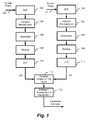
- FIG. 1 shows a block representation of a process for generating an impedance estimate in an active transmitter of an antenna coupled to the transmitter.
- the voltage 100 and current 101 samples are measured using probes such as a transformer-coupled current probe and a capacitive attenuator voltage probe.
- the probes sample the modulating live broadcast signal across the range of frequency content. The sampling rate does not need any particular relationship to the carrier frequency of the modulated signal.
- both the voltage 100 and current 101 samples can be processed through independent parallel paths.
- the voltage 100 and current 101 are then sampled using analog-to-digital converters (ADC) 102 and 103 for each probe.
- ADC analog-to-digital converters
- the voltage 100 and current 101 could be calculated from alternative samples captured using appropriate probes.
- directional couplers could be used to measure the forward and reflected voltage.
- voltage would be calculated by the sum of these samples and the current determined by the difference in the samples. This calculation can either be made on the analog samples, or at any point before the complex division 112.
- complex demodulation 104 and 105 is performed on each sample in order to shift the samples 100 and101 from radio frequency back to baseband. This shift can be accomplished by multiplying a complex phasor at the carrier frequency. Alternatively, if the carrier frequency is low enough, the demodulation 104 and 105 can be bypassed. In this case, the resulting impedance measurement will be centered around baseband, rather than at the carrier frequency.
- the signals are further processed by decimation at 106 and 107.
- decimation at 106 and 107 the signals are passed through a low pass filter and then down-sampled to lower sampling rate.
- DFTs discrete Fourier transforms
- the amount of decimation required is dependent on the ADC bandwidth (number of bits) and sampling rate. A higher sampling rate will require more decimation of the samples before the FFT is applied.
- the impedance measurements are calculated by using blocks of samples.
- the block length determines the computational requirements and the frequency of resolution that is obtained. For most antennas, the impedance will typically not vary dramatically over the pass band, so a block length that gives a reasonable number of sample points is appropriate.
- the sampling of these blocks will also affect the exact time domain points used to determine the impedance.
- Representative sampling methods include an overlapping window approach, such as that commonly used for power spectral density estimations, and random sampling. An overlapping window approach may be used in order to provide a more accurate estimation of the relative frequency content of the two time domain signals.
- window functions 108 and 109 for this application include high-valued Kaiser windows, Blackmann-Harris window, Nuttall window, or similar low-resolution (high-dynamic-range) window. However, based on the type of signal, any one of a number of windows could be applied. For example, if the signal has sufficient frequency content at all desired measurement frequencies, a window with less dynamic range may be used.
- the windowing may be bypassed entirely if the signal permits a rectangular window to be used, although some degradation to the resulting impedance measurement may occur.
- a discrete Fourier transform such as a finite Fourier transform (FFT) 110 and 111 to extract the phase and amplitude of each frequency component on both the voltage and current samples for each block.
- DFT discrete Fourier transform
- FFT finite Fourier transform
- the fast Fourier transform can be applied to extract the phase and amplitude of each frequency component, however, based on the type of signal, other methods can be employed to extract this information.
- the resulting frequency domains for the voltage and the current can be used to determine an approximate value for the impedance in which the transmitter is feeding into.
- the impedance at each frequency can be obtained by dividing the frequency domain value for the voltage by the frequency domain value of the current (represented by block 112).
- additional equations or data manipulation may be required to obtain the impedance.
- the accuracy of impedance measurement is highly dependent on the level of frequency content present in the sampled block. Accordingly, the estimates must be averaged to obtain a reasonably accurate measurement. To achieve such an average, a first-order decaying exponential filter with an adequate delay can be applied. Similar-type filters could be applied to the estimates in order to achieve a reasonably accurate measurement.
- the signal being used for the estimate is not a training signal or known signal, there may be frequencies that have either intermittent or no signal content. If the impedance calculation is performed and there is not enough signal content, then the estimate will be inaccurate at those frequencies. In these cases, intelligent averaging and interpolation 113 is applied to mitigate this effect. There are several different ways this can be accomplished. For example, if the signal intermittently has content at all frequencies, the impedance estimate can be managed by making the weighting of the average proportional to the signal power present in that block at each frequency. Using this method, the points with the most power at a particular frequency will have the most influence on the impedance estimate at that frequency. However, situations will still arise where there is no power at all, at certain frequencies. If there is no signal content at the frequency in question, and no reasonable estimate can be obtained for the impedance, a value can potentially be interpolated from other known points.
- FIG. 2 shows a transmitter 200 providing impedance measurement capability.
- a signal source 202 provides a broadcast or audio input to the transmitter 200 and the modulation chain 201.
- a digital modulator 204 modulates the incoming signal to the desired modulation.
- the modulating signal is then up-converted by a synthesized frequency source 206 to the desired carrier frequency.
- the resulting signal is then filtered by a band-pass filter 208, such as a dual band-pass filter, to remove unwanted frequency components.
- the signal is then amplified by one or more power amplifiers 210.
- a transmission line connects the transmitter 200 to a tuning or load matching network 212 to provide impedance matching with an antenna 214.
- the tuning network 212 is typically adjusted by using a test signal and lower power test equipment to calculate an impedance estimate.
- samples of the amplified signal prior in the transmission line to the tuning network 212 are sampled using voltage and current probes 220 and 222.
- the probes may alternatively be directional couplers.
- the directional couplers measure the forward and reverse voltage waves in the transmission line, whereas the voltage probe measures the voltage just at that point in the line, and the current probe measures the current at that point. If the load is perfect (for example: resistive 50 ohm load) then the voltage and current measured at different lengths along the transmission line would be the same. If not, a high and low points in both voltage and current result, determined by the voltage standing wave ratio.
- the directional sample is better, since all that is needed is the forward voltage to make that measurement.
- FM higher frequency
- directional couplers are more common than pure voltage or current samples, and are typically coupled off using the geometry of the probe, rather than a transformer or capacitor. The relationship is that the forward voltage is the sum of the current and voltage samples at any point on the transmission line, and the reverse voltage is the difference.
- the voltage 220 and current 222 probe or coupler provide an analog output to analog to digital converters (ADCs) 224 and 226 respectively.
- the digital output is then demodulated using complex demodulation using the down-conversion module 228.
- Complex demodulation may be performed using a processor such as a digital signal processor (DSP), field programmable gate array (FPGA) or application specific integrated circuit (ASIC).
- DSP digital signal processor
- FPGA field programmable gate array
- ASIC application specific integrated circuit
- the down-conversion module 228 can also provide decimation of the samples prior to passing through a low pass filter 230 to remove the -2 f c .
- the decimation process down-samples the demodulated digital signals to a lower sampling rate. After filtering has been performed the remaining frequency data is processed by a signal processing module 232.
- the signal processing module 232 may be implemented by one or more processor, DSP's, FPGA's, or ASICs or a combination thereof.
- the signal processing module 232 can then implement processing of the samples such as by using a FFT to extract phase and amplitude of each frequency component for both the voltage and current samples for each block.
- the signal processing module 232 may perform adaptive filtering using a finite impulse response (FIR), filter such as Least Mean Squares and zero padding the FIR result to generate an impedance estimate.
- FIR finite impulse response
- the resulting FIR structure produces a filter with the same amplitude and phase response as the antenna load.
- the resulting impedance data can then be further processed by processor 234, for either providing pre-distortion data to digital modulator 204, providing control of the tuning network or tuning values for use by the tuning network 212 to improve transmission efficiency and performance.
- the data may be provided to an external data processing system such as a computer 250 for further trending or storage on storage device 252. Again, this data may be utilized to control the load matching network 212.
- a computer or processor readable memory 236 may be used by the processors of down-conversion module 228, signal processing module 232 or processor module 234 to enable access to software code or instructions, determine data value, configuration parameters or operating characteristics.
- the memory 234 may be embodied in random access memory, read only memory, nonvolatile memory such as flash memory.
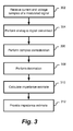
- FIG. 3 shows a method of generating an impedance estimate in an active transmitter.
- the method commences with receiving voltage and current samples of a modulating signal 302 from a transmission line between a transmitter 200 and an antenna 214 using voltage and current probes 220 and 222.
- the sampling is provided at a fixed sampling rate independent of the carrier frequency of the RF transmission.
- Analog to digital down conversion is then performed at 304 of voltage and current samples by ADCs 224 and 226.
- the samples may be converted in parallel or sequentially depending on the implementation of the ADC converters.
- Complex demodulation is then performed on the digital samples at 306 by down-conversion module 228.
- the demodulated samples are decimated at 308 to reduce the number of samples to be processed.
- the estimate may also be filtered using a low pass filter 230.
- the impedance estimate can by generated by performing impedance calculations using the voltage and frequency samples by signal processing unit 232.
- the impedance estimate may be determined using frequency domains for the voltage and current samples as described in Figure 4 or by determining a frequency response between current and voltage samples using a time domain adaptive filtering method as described in Figure 5 .
- the impedance estimate can then be provided to internal processor 234 or external computing device 250 at 312 for further processing or storage.
- the resulting estimate may then be provided to load matching network or digital modulator 204 to improve performance of the transmitter 200.
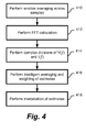
- Figure 4 shows a method of calculating an impedance estimate in an active transmitter using a fast Fourier transform (FFT) as implemented at 310 of Figure 3 .
- the signal processing unit 232 at 410 can, after decimation and filtering is performed at 308, apply a windowing function for averaging across the samples based upon the type of transmitted signal. Windowing is applied to shape the time portion of sample data, to minimize edge effects that result in spectral leakage in the FFT spectrum. By using window functions correctly, the spectral resolution of the frequency-domain result will increase. Windowing is required when using a broadcast signal due to the large carrier frequency component.
- the modulating signal content is typically anywhere from 15 to 50 dB lower, so getting an accurate measurement without it would be unfeasible.
- Appropriate windowing functions for this application include high-valued Kaiser windows, Blackmann-Harris window, Nuttall window, or similar low-resolution (high-dynamic-range) windowing techniques. However, based on the type of signal, any one of a number of windowing techniques could be applied. Similarly windowing may be bypassed if it is not required for the signal being analyzed.
- a FFT calculation is then performed on the data to extract the phase and amplitude of each frequency component on both the voltage and current samples at 412. Complex division of V(f) and I(f) can then be performed to generate the impedance estimates for the modulating signal at 414.
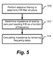
- FIG. 5 shows a method of calculating an impedance estimate in an active transmitter using time domain adaptive filtering as implemented at 310 of Figure 3 .
- the frequency response between current and voltage can be determined using a time domain adaptive filtering method.
- decimation at 308 the current samples and a delayed version of the voltage samples are passed into an adaptive finite impulse response (FIR) filtering process, such as Least Mean Squares (LMS) at 510.
- FIR finite impulse response
- LMS Least Mean Squares
- Other adaptive FIR algorithms could also be used.
- the current samples are taken to be the input to this process, with the delayed voltage samples representing the desired signal.
- the filtering process adapts the resulting FIR structure, it will produce a filter with the same amplitude and phase response as the load, with some additional delay.
- the adaptive filtering process is inherently averaging, so the impedance measured by this method would not require any further averaging.
- the impedance estimate of the load can be determined by zero-padding the filter and taking a DFT (or FFT) at 512. This provides a complex response of the load versus frequency.
- the additional delay added to the voltage vector in the adaptive filtering process must be removed at 514 to get an accurate phase measurement. This can be accomplished by converting the delay to the appropriate phase at each frequency and canceling it.
- the resulting estimate can than be provided at 312.
- a computer readable memory may be utilized to store instructions of the described method for execution by a processor, DSP or ASIC.
Landscapes
- Engineering & Computer Science (AREA)
- Computer Networks & Wireless Communication (AREA)
- Signal Processing (AREA)
- Physics & Mathematics (AREA)
- Electromagnetism (AREA)
- Transmitters (AREA)
- Measurement Of Resistance Or Impedance (AREA)
- Amplitude Modulation (AREA)
Applications Claiming Priority (1)
| Application Number | Priority Date | Filing Date | Title |
|---|---|---|---|
| US4421308P | 2008-04-11 | 2008-04-11 |
Publications (3)
| Publication Number | Publication Date |
|---|---|
| EP2109224A2 true EP2109224A2 (fr) | 2009-10-14 |
| EP2109224A3 EP2109224A3 (fr) | 2014-03-12 |
| EP2109224B1 EP2109224B1 (fr) | 2019-05-22 |
Family
ID=40847054
Family Applications (1)
| Application Number | Title | Priority Date | Filing Date |
|---|---|---|---|
| EP09157880.7A Active EP2109224B1 (fr) | 2008-04-11 | 2009-04-14 | Mesure d'impédance dans un transmetteur de fréquence radio actif |
Country Status (3)
| Country | Link |
|---|---|
| US (2) | US8213885B2 (fr) |
| EP (1) | EP2109224B1 (fr) |
| TR (1) | TR201910525T4 (fr) |
Cited By (3)
| Publication number | Priority date | Publication date | Assignee | Title |
|---|---|---|---|---|
| US9584191B2 (en) | 2013-12-20 | 2017-02-28 | Southern Avionics Co. | Antenna tuning unit |
| EP3297408A4 (fr) * | 2015-06-11 | 2019-02-20 | Southwestern Institute of Physics | Procédé et système de calcul en temps réel de signal de déphasage, procédé et système de diagnostic de plasma |
| CN112272032A (zh) * | 2020-10-15 | 2021-01-26 | 沈阳安费诺三浦汽车电子有限公司 | V2x有源收发天线、v2x有源接收天线及集成天线 |
Families Citing this family (17)
| Publication number | Priority date | Publication date | Assignee | Title |
|---|---|---|---|---|
| US8213885B2 (en) | 2008-04-11 | 2012-07-03 | Nautel Limited | Impedance measurement in an active radio frequency transmitter |
| US9203489B2 (en) | 2010-05-05 | 2015-12-01 | Google Technology Holdings LLC | Method and precoder information feedback in multi-antenna wireless communication systems |
| US20120027058A1 (en) * | 2010-07-29 | 2012-02-02 | The Regents Of The University Of Michigan | Portable, wireless multi-channel impedance analyzer |
| US8674782B2 (en) * | 2011-03-31 | 2014-03-18 | Texas Instruments Incorporated | RF impedance detection using two point voltage sampling |
| US9392558B2 (en) * | 2012-06-08 | 2016-07-12 | Qualcomm Incorporated | Control of transmit power and adjustment of antenna tuning network of a wireless device |
| US9813262B2 (en) | 2012-12-03 | 2017-11-07 | Google Technology Holdings LLC | Method and apparatus for selectively transmitting data using spatial diversity |
| US9591508B2 (en) | 2012-12-20 | 2017-03-07 | Google Technology Holdings LLC | Methods and apparatus for transmitting data between different peer-to-peer communication groups |
| US9979531B2 (en) | 2013-01-03 | 2018-05-22 | Google Technology Holdings LLC | Method and apparatus for tuning a communication device for multi band operation |
| US10229697B2 (en) | 2013-03-12 | 2019-03-12 | Google Technology Holdings LLC | Apparatus and method for beamforming to obtain voice and noise signals |
| US9386542B2 (en) | 2013-09-19 | 2016-07-05 | Google Technology Holdings, LLC | Method and apparatus for estimating transmit power of a wireless device |
| US9549290B2 (en) | 2013-12-19 | 2017-01-17 | Google Technology Holdings LLC | Method and apparatus for determining direction information for a wireless device |
| US9491007B2 (en) | 2014-04-28 | 2016-11-08 | Google Technology Holdings LLC | Apparatus and method for antenna matching |
| US9478847B2 (en) | 2014-06-02 | 2016-10-25 | Google Technology Holdings LLC | Antenna system and method of assembly for a wearable electronic device |
| FR3091089B1 (fr) * | 2018-12-19 | 2022-03-11 | Commissariat Energie Atomique | Dispositif de transmission acoustique |
| CN116235060B (zh) * | 2020-07-29 | 2025-08-22 | 技术应用股份公司 | 接地系统的阻抗测量 |
| US12047757B2 (en) * | 2021-11-09 | 2024-07-23 | Cirrus Logic Inc. | Windowing filter for amplifier device |
| US20250337505A1 (en) * | 2024-04-30 | 2025-10-30 | Microsoft Technology Licensing, Llc | Adjusting a transmission signal |
Family Cites Families (28)
| Publication number | Priority date | Publication date | Assignee | Title |
|---|---|---|---|---|
| GB2178616B (en) | 1985-07-26 | 1989-04-26 | Marconi Co Ltd | Impedance matching arrangement |
| US4965607A (en) * | 1987-04-30 | 1990-10-23 | Br Communications, Inc. | Antenna coupler |
| US5247470A (en) * | 1987-07-29 | 1993-09-21 | E-Systems, Inc. | Method and apparatus for estimating signal components of a filter output |
| US4967159A (en) | 1989-02-23 | 1990-10-30 | Abbott Laboratories | Self-balancing reflectometer |
| US5386194A (en) * | 1991-10-18 | 1995-01-31 | Harris Corporation | Digital impedance determination using peak detection of current and voltage samplers |
| US5206600A (en) | 1991-10-18 | 1993-04-27 | Harris Corporation | Impedance determining apparatus using quadrature current and peak detectors |
| US5458732A (en) * | 1992-04-14 | 1995-10-17 | Texas Instruments Incorporated | Method and system for identifying process conditions |
| US5565737A (en) * | 1995-06-07 | 1996-10-15 | Eni - A Division Of Astec America, Inc. | Aliasing sampler for plasma probe detection |
| US6032028A (en) * | 1996-04-12 | 2000-02-29 | Continentral Electronics Corporation | Radio transmitter apparatus and method |
| US5770922A (en) * | 1996-07-22 | 1998-06-23 | Eni Technologies, Inc. | Baseband V-I probe |
| US5931892A (en) * | 1996-12-20 | 1999-08-03 | Compaq Computer Corporation | Enhanced adaptive filtering technique |
| US6005398A (en) | 1997-09-26 | 1999-12-21 | Rockwell Science Center, Inc. | High speed phase and amplitude measurement system and method |
| FR2797957B1 (fr) * | 1999-08-24 | 2001-11-16 | Thomson Csf | Procede et dispositif pour la mesure d'impedance d'antenne |
| EP1385439A1 (fr) * | 2001-05-10 | 2004-02-04 | Rita Medical Systems, Inc. | Appareil et procede d'ablation tissulaire par rf |
| AU2003250755A1 (en) * | 2002-06-18 | 2003-12-31 | Automotive Distance Control Systems Gmbh | Circuit arrangement for generating an iq signal |
| US6707255B2 (en) * | 2002-07-10 | 2004-03-16 | Eni Technology, Inc. | Multirate processing for metrology of plasma RF source |
| EP1547117A4 (fr) * | 2002-09-23 | 2010-04-07 | Turner Entpr & Associates | Ensemble transducteur servant a commander des processus |
| KR101058733B1 (ko) * | 2004-01-02 | 2011-08-22 | 삼성전자주식회사 | 전력 증폭기의 비선형 왜곡 특성을 보상하는 전치보상 장치 |
| US7379714B2 (en) | 2004-04-02 | 2008-05-27 | Interdigital Technology Corporation | Method and apparatus for dynamically adjusting a transmitter's impedance |
| US7602127B2 (en) * | 2005-04-18 | 2009-10-13 | Mks Instruments, Inc. | Phase and frequency control of a radio frequency generator from an external source |
| US7151382B1 (en) * | 2005-09-22 | 2006-12-19 | Rockwell Collins, Inc. | Apparatus and method for radio frequency power and standing wave ratio measurement |
| US7774396B2 (en) * | 2005-11-18 | 2010-08-10 | Dynamic Hearing Pty Ltd | Method and device for low delay processing |
| US7489145B2 (en) | 2005-12-14 | 2009-02-10 | Daihen Corporation | Plasma processing system |
| DE102006031053A1 (de) * | 2006-07-05 | 2008-01-10 | Rohde & Schwarz Gmbh & Co. Kg | Anordnung zum Bestimmen der Betriebskenngrößen eines Hochfrequenz-Leistungsverstärkers |
| KR100758206B1 (ko) | 2006-09-14 | 2007-09-12 | 주식회사 쏠리테크 | 반향성분 제거 시스템 및 반향성분 제거방법 |
| US7629795B2 (en) * | 2007-07-30 | 2009-12-08 | John D. Terleski | Vector impedance measurement system and method of using same |
| FR2920927B1 (fr) | 2007-09-11 | 2011-05-06 | Commissariat Energie Atomique | Procede d'adaptation automatique d'impedance de circuit radiofrequence et chaine d'emission ou reception a adaptation automatique |
| US8213885B2 (en) | 2008-04-11 | 2012-07-03 | Nautel Limited | Impedance measurement in an active radio frequency transmitter |
-
2009
- 2009-04-09 US US12/421,519 patent/US8213885B2/en active Active
- 2009-04-14 EP EP09157880.7A patent/EP2109224B1/fr active Active
- 2009-04-14 TR TR2019/10525T patent/TR201910525T4/tr unknown
-
2012
- 2012-03-06 US US13/412,661 patent/US8452245B2/en active Active
Cited By (3)
| Publication number | Priority date | Publication date | Assignee | Title |
|---|---|---|---|---|
| US9584191B2 (en) | 2013-12-20 | 2017-02-28 | Southern Avionics Co. | Antenna tuning unit |
| EP3297408A4 (fr) * | 2015-06-11 | 2019-02-20 | Southwestern Institute of Physics | Procédé et système de calcul en temps réel de signal de déphasage, procédé et système de diagnostic de plasma |
| CN112272032A (zh) * | 2020-10-15 | 2021-01-26 | 沈阳安费诺三浦汽车电子有限公司 | V2x有源收发天线、v2x有源接收天线及集成天线 |
Also Published As
| Publication number | Publication date |
|---|---|
| TR201910525T4 (tr) | 2019-08-21 |
| US8213885B2 (en) | 2012-07-03 |
| EP2109224A3 (fr) | 2014-03-12 |
| US20120170632A1 (en) | 2012-07-05 |
| US20090258614A1 (en) | 2009-10-15 |
| US8452245B2 (en) | 2013-05-28 |
| EP2109224B1 (fr) | 2019-05-22 |
Similar Documents
| Publication | Publication Date | Title |
|---|---|---|
| EP2109224B1 (fr) | Mesure d'impédance dans un transmetteur de fréquence radio actif | |
| US11387920B2 (en) | Methods and apparatuses for measuring the distance to a passive intermodulation source | |
| EP3016291B1 (fr) | Procédé d'atténuation adaptative des interférences dans un spectre à large bande | |
| CN111835434B (zh) | 一种宽带频率响应的测量方法及其测量装置 | |
| US9482705B2 (en) | Measurement of voltage standing wave ratio of antenna system | |
| US8837653B2 (en) | High frequency signal receiver with self-calibrated group delay compensation | |
| CN109257051B (zh) | 一种数字信道化射频存储系统 | |
| US8837654B2 (en) | Signal receiver with group delay and amplitude distortion compensation | |
| CN106664148B (zh) | 同时呼叫传输检测 | |
| CN103837740A (zh) | 一种高精度数字瞬时测频方法及装置 | |
| CN117997455B (zh) | 一种计算群时延测量相位的方法及系统 | |
| CN119535115A (zh) | 一种多通道漏泄同轴电缆故障定位系统及方法 | |
| US9654233B2 (en) | VSWR estimation using spectral analysis to suppress external interference | |
| US7161511B2 (en) | Linearization system and method | |
| CN116388897A (zh) | 一种全数字超宽带测频测向系统及其使用方法 | |
| CN1968161B (zh) | 一种模拟信号通道的滤波均衡的方法 | |
| US9813134B1 (en) | Base station and antenna calibration method | |
| CN118688777B (zh) | 一种应用于干扰信道场景的多载波相位测距方法 | |
| CN116566415B (zh) | 超宽带不平坦和iq不平衡的校准方法、装置、介质及设备 | |
| CN115494464A (zh) | 线性调频信号的预失真补偿方法、电子设备及存储介质 | |
| JP2009276247A (ja) | レーダ信号処理装置 | |
| CN114844579B (zh) | 基于窄带滤波器的时域统计qec校准方法及装置 | |
| CN119544104B (zh) | 数字相控阵接收通道相位非线性的测量方法、装置及设备 | |
| Peltola | Design of a software defined radio spectrometer for space applications | |
| WO2005036771A1 (fr) | Procede et appareil de determination d'un retard |
Legal Events
| Date | Code | Title | Description |
|---|---|---|---|
| PUAI | Public reference made under article 153(3) epc to a published international application that has entered the european phase |
Free format text: ORIGINAL CODE: 0009012 |
|
| AK | Designated contracting states |
Kind code of ref document: A2 Designated state(s): AT BE BG CH CY CZ DE DK EE ES FI FR GB GR HR HU IE IS IT LI LT LU LV MC MK MT NL NO PL PT RO SE SI SK TR |
|
| PUAL | Search report despatched |
Free format text: ORIGINAL CODE: 0009013 |
|
| AK | Designated contracting states |
Kind code of ref document: A3 Designated state(s): AT BE BG CH CY CZ DE DK EE ES FI FR GB GR HR HU IE IS IT LI LT LU LV MC MK MT NL NO PL PT RO SE SI SK TR |
|
| AX | Request for extension of the european patent |
Extension state: AL BA RS |
|
| RIC1 | Information provided on ipc code assigned before grant |
Ipc: H04B 1/04 20060101AFI20140204BHEP |
|
| 17P | Request for examination filed |
Effective date: 20140906 |
|
| RBV | Designated contracting states (corrected) |
Designated state(s): AT BE BG CH CY CZ DE DK EE ES FI FR GB GR HR HU IE IS IT LI LT LU LV MC MK MT NL NO PL PT RO SE SI SK TR |
|
| 17Q | First examination report despatched |
Effective date: 20150703 |
|
| GRAP | Despatch of communication of intention to grant a patent |
Free format text: ORIGINAL CODE: EPIDOSNIGR1 |
|
| STAA | Information on the status of an ep patent application or granted ep patent |
Free format text: STATUS: GRANT OF PATENT IS INTENDED |
|
| INTG | Intention to grant announced |
Effective date: 20181129 |
|
| GRAS | Grant fee paid |
Free format text: ORIGINAL CODE: EPIDOSNIGR3 |
|
| GRAA | (expected) grant |
Free format text: ORIGINAL CODE: 0009210 |
|
| STAA | Information on the status of an ep patent application or granted ep patent |
Free format text: STATUS: THE PATENT HAS BEEN GRANTED |
|
| AK | Designated contracting states |
Kind code of ref document: B1 Designated state(s): AT BE BG CH CY CZ DE DK EE ES FI FR GB GR HR HU IE IS IT LI LT LU LV MC MK MT NL NO PL PT RO SE SI SK TR |
|
| REG | Reference to a national code |
Ref country code: GB Ref legal event code: FG4D |
|
| REG | Reference to a national code |
Ref country code: CH Ref legal event code: EP |
|
| REG | Reference to a national code |
Ref country code: IE Ref legal event code: FG4D |
|
| REG | Reference to a national code |
Ref country code: DE Ref legal event code: R096 Ref document number: 602009058435 Country of ref document: DE |
|
| REG | Reference to a national code |
Ref country code: AT Ref legal event code: REF Ref document number: 1137323 Country of ref document: AT Kind code of ref document: T Effective date: 20190615 |
|
| REG | Reference to a national code |
Ref country code: NO Ref legal event code: T2 Effective date: 20190522 |
|
| REG | Reference to a national code |
Ref country code: SE Ref legal event code: TRGR |
|
| REG | Reference to a national code |
Ref country code: NL Ref legal event code: MP Effective date: 20190522 |
|
| REG | Reference to a national code |
Ref country code: LT Ref legal event code: MG4D |
|
| REG | Reference to a national code |
Ref country code: GR Ref legal event code: EP Ref document number: 20190402186 Country of ref document: GR Effective date: 20191016 |
|
| PG25 | Lapsed in a contracting state [announced via postgrant information from national office to epo] |
Ref country code: FI Free format text: LAPSE BECAUSE OF FAILURE TO SUBMIT A TRANSLATION OF THE DESCRIPTION OR TO PAY THE FEE WITHIN THE PRESCRIBED TIME-LIMIT Effective date: 20190522 Ref country code: LT Free format text: LAPSE BECAUSE OF FAILURE TO SUBMIT A TRANSLATION OF THE DESCRIPTION OR TO PAY THE FEE WITHIN THE PRESCRIBED TIME-LIMIT Effective date: 20190522 Ref country code: HR Free format text: LAPSE BECAUSE OF FAILURE TO SUBMIT A TRANSLATION OF THE DESCRIPTION OR TO PAY THE FEE WITHIN THE PRESCRIBED TIME-LIMIT Effective date: 20190522 Ref country code: ES Free format text: LAPSE BECAUSE OF FAILURE TO SUBMIT A TRANSLATION OF THE DESCRIPTION OR TO PAY THE FEE WITHIN THE PRESCRIBED TIME-LIMIT Effective date: 20190522 Ref country code: NL Free format text: LAPSE BECAUSE OF FAILURE TO SUBMIT A TRANSLATION OF THE DESCRIPTION OR TO PAY THE FEE WITHIN THE PRESCRIBED TIME-LIMIT Effective date: 20190522 Ref country code: PT Free format text: LAPSE BECAUSE OF FAILURE TO SUBMIT A TRANSLATION OF THE DESCRIPTION OR TO PAY THE FEE WITHIN THE PRESCRIBED TIME-LIMIT Effective date: 20190922 |
|
| PG25 | Lapsed in a contracting state [announced via postgrant information from national office to epo] |
Ref country code: LV Free format text: LAPSE BECAUSE OF FAILURE TO SUBMIT A TRANSLATION OF THE DESCRIPTION OR TO PAY THE FEE WITHIN THE PRESCRIBED TIME-LIMIT Effective date: 20190522 Ref country code: BG Free format text: LAPSE BECAUSE OF FAILURE TO SUBMIT A TRANSLATION OF THE DESCRIPTION OR TO PAY THE FEE WITHIN THE PRESCRIBED TIME-LIMIT Effective date: 20190822 |
|
| REG | Reference to a national code |
Ref country code: AT Ref legal event code: MK05 Ref document number: 1137323 Country of ref document: AT Kind code of ref document: T Effective date: 20190522 |
|
| PG25 | Lapsed in a contracting state [announced via postgrant information from national office to epo] |
Ref country code: RO Free format text: LAPSE BECAUSE OF FAILURE TO SUBMIT A TRANSLATION OF THE DESCRIPTION OR TO PAY THE FEE WITHIN THE PRESCRIBED TIME-LIMIT Effective date: 20190522 Ref country code: CZ Free format text: LAPSE BECAUSE OF FAILURE TO SUBMIT A TRANSLATION OF THE DESCRIPTION OR TO PAY THE FEE WITHIN THE PRESCRIBED TIME-LIMIT Effective date: 20190522 Ref country code: SK Free format text: LAPSE BECAUSE OF FAILURE TO SUBMIT A TRANSLATION OF THE DESCRIPTION OR TO PAY THE FEE WITHIN THE PRESCRIBED TIME-LIMIT Effective date: 20190522 Ref country code: DK Free format text: LAPSE BECAUSE OF FAILURE TO SUBMIT A TRANSLATION OF THE DESCRIPTION OR TO PAY THE FEE WITHIN THE PRESCRIBED TIME-LIMIT Effective date: 20190522 Ref country code: AT Free format text: LAPSE BECAUSE OF FAILURE TO SUBMIT A TRANSLATION OF THE DESCRIPTION OR TO PAY THE FEE WITHIN THE PRESCRIBED TIME-LIMIT Effective date: 20190522 Ref country code: EE Free format text: LAPSE BECAUSE OF FAILURE TO SUBMIT A TRANSLATION OF THE DESCRIPTION OR TO PAY THE FEE WITHIN THE PRESCRIBED TIME-LIMIT Effective date: 20190522 |
|
| REG | Reference to a national code |
Ref country code: DE Ref legal event code: R097 Ref document number: 602009058435 Country of ref document: DE |
|
| PG25 | Lapsed in a contracting state [announced via postgrant information from national office to epo] |
Ref country code: IT Free format text: LAPSE BECAUSE OF FAILURE TO SUBMIT A TRANSLATION OF THE DESCRIPTION OR TO PAY THE FEE WITHIN THE PRESCRIBED TIME-LIMIT Effective date: 20190522 |
|
| PLBE | No opposition filed within time limit |
Free format text: ORIGINAL CODE: 0009261 |
|
| STAA | Information on the status of an ep patent application or granted ep patent |
Free format text: STATUS: NO OPPOSITION FILED WITHIN TIME LIMIT |
|
| 26N | No opposition filed |
Effective date: 20200225 |
|
| PG25 | Lapsed in a contracting state [announced via postgrant information from national office to epo] |
Ref country code: PL Free format text: LAPSE BECAUSE OF FAILURE TO SUBMIT A TRANSLATION OF THE DESCRIPTION OR TO PAY THE FEE WITHIN THE PRESCRIBED TIME-LIMIT Effective date: 20190522 |
|
| PG25 | Lapsed in a contracting state [announced via postgrant information from national office to epo] |
Ref country code: SI Free format text: LAPSE BECAUSE OF FAILURE TO SUBMIT A TRANSLATION OF THE DESCRIPTION OR TO PAY THE FEE WITHIN THE PRESCRIBED TIME-LIMIT Effective date: 20190522 |
|
| REG | Reference to a national code |
Ref country code: DE Ref legal event code: R119 Ref document number: 602009058435 Country of ref document: DE |
|
| PG25 | Lapsed in a contracting state [announced via postgrant information from national office to epo] |
Ref country code: MC Free format text: LAPSE BECAUSE OF FAILURE TO SUBMIT A TRANSLATION OF THE DESCRIPTION OR TO PAY THE FEE WITHIN THE PRESCRIBED TIME-LIMIT Effective date: 20190522 |
|
| REG | Reference to a national code |
Ref country code: CH Ref legal event code: PL |
|
| PG25 | Lapsed in a contracting state [announced via postgrant information from national office to epo] |
Ref country code: CH Free format text: LAPSE BECAUSE OF NON-PAYMENT OF DUE FEES Effective date: 20200430 Ref country code: LU Free format text: LAPSE BECAUSE OF NON-PAYMENT OF DUE FEES Effective date: 20200414 Ref country code: FR Free format text: LAPSE BECAUSE OF NON-PAYMENT OF DUE FEES Effective date: 20200430 Ref country code: LI Free format text: LAPSE BECAUSE OF NON-PAYMENT OF DUE FEES Effective date: 20200430 Ref country code: DE Free format text: LAPSE BECAUSE OF NON-PAYMENT OF DUE FEES Effective date: 20201103 |
|
| REG | Reference to a national code |
Ref country code: BE Ref legal event code: MM Effective date: 20200430 |
|
| PG25 | Lapsed in a contracting state [announced via postgrant information from national office to epo] |
Ref country code: BE Free format text: LAPSE BECAUSE OF NON-PAYMENT OF DUE FEES Effective date: 20200430 |
|
| PG25 | Lapsed in a contracting state [announced via postgrant information from national office to epo] |
Ref country code: IE Free format text: LAPSE BECAUSE OF NON-PAYMENT OF DUE FEES Effective date: 20200414 |
|
| PG25 | Lapsed in a contracting state [announced via postgrant information from national office to epo] |
Ref country code: MT Free format text: LAPSE BECAUSE OF FAILURE TO SUBMIT A TRANSLATION OF THE DESCRIPTION OR TO PAY THE FEE WITHIN THE PRESCRIBED TIME-LIMIT Effective date: 20190522 Ref country code: CY Free format text: LAPSE BECAUSE OF FAILURE TO SUBMIT A TRANSLATION OF THE DESCRIPTION OR TO PAY THE FEE WITHIN THE PRESCRIBED TIME-LIMIT Effective date: 20190522 |
|
| PG25 | Lapsed in a contracting state [announced via postgrant information from national office to epo] |
Ref country code: MK Free format text: LAPSE BECAUSE OF FAILURE TO SUBMIT A TRANSLATION OF THE DESCRIPTION OR TO PAY THE FEE WITHIN THE PRESCRIBED TIME-LIMIT Effective date: 20190522 Ref country code: IS Free format text: LAPSE BECAUSE OF FAILURE TO SUBMIT A TRANSLATION OF THE DESCRIPTION OR TO PAY THE FEE WITHIN THE PRESCRIBED TIME-LIMIT Effective date: 20190922 |
|
| PGFP | Annual fee paid to national office [announced via postgrant information from national office to epo] |
Ref country code: SE Payment date: 20220411 Year of fee payment: 14 Ref country code: NO Payment date: 20220411 Year of fee payment: 14 Ref country code: GB Payment date: 20220407 Year of fee payment: 14 |
|
| PGFP | Annual fee paid to national office [announced via postgrant information from national office to epo] |
Ref country code: GR Payment date: 20220420 Year of fee payment: 14 |
|
| REG | Reference to a national code |
Ref country code: NO Ref legal event code: MMEP |
|
| REG | Reference to a national code |
Ref country code: SE Ref legal event code: EUG |
|
| GBPC | Gb: european patent ceased through non-payment of renewal fee |
Effective date: 20230414 |
|
| PG25 | Lapsed in a contracting state [announced via postgrant information from national office to epo] |
Ref country code: GB Free format text: LAPSE BECAUSE OF NON-PAYMENT OF DUE FEES Effective date: 20230414 Ref country code: GR Free format text: LAPSE BECAUSE OF NON-PAYMENT OF DUE FEES Effective date: 20231110 |
|
| PG25 | Lapsed in a contracting state [announced via postgrant information from national office to epo] |
Ref country code: SE Free format text: LAPSE BECAUSE OF NON-PAYMENT OF DUE FEES Effective date: 20230415 Ref country code: NO Free format text: LAPSE BECAUSE OF NON-PAYMENT OF DUE FEES Effective date: 20230430 Ref country code: GR Free format text: LAPSE BECAUSE OF NON-PAYMENT OF DUE FEES Effective date: 20231110 Ref country code: GB Free format text: LAPSE BECAUSE OF NON-PAYMENT OF DUE FEES Effective date: 20230414 |
|
| PGFP | Annual fee paid to national office [announced via postgrant information from national office to epo] |
Ref country code: TR Payment date: 20250404 Year of fee payment: 17 |