EP2110849A2 - Verbindungsstruktur mit Hybridrahmenplatte - Google Patents
Verbindungsstruktur mit Hybridrahmenplatte Download PDFInfo
- Publication number
- EP2110849A2 EP2110849A2 EP09157431A EP09157431A EP2110849A2 EP 2110849 A2 EP2110849 A2 EP 2110849A2 EP 09157431 A EP09157431 A EP 09157431A EP 09157431 A EP09157431 A EP 09157431A EP 2110849 A2 EP2110849 A2 EP 2110849A2
- Authority
- EP
- European Patent Office
- Prior art keywords
- region
- insulative layer
- electronic device
- base insulative
- frame panel
- Prior art date
- Legal status (The legal status is an assumption and is not a legal conclusion. Google has not performed a legal analysis and makes no representation as to the accuracy of the status listed.)
- Ceased
Links
Images

Classifications
-
- H—ELECTRICITY
- H10—SEMICONDUCTOR DEVICES; ELECTRIC SOLID-STATE DEVICES NOT OTHERWISE PROVIDED FOR
- H10W—GENERIC PACKAGES, INTERCONNECTIONS, CONNECTORS OR OTHER CONSTRUCTIONAL DETAILS OF DEVICES COVERED BY CLASS H10
- H10W99/00—Subject matter not provided for in other groups of this subclass
-
- H—ELECTRICITY
- H10—SEMICONDUCTOR DEVICES; ELECTRIC SOLID-STATE DEVICES NOT OTHERWISE PROVIDED FOR
- H10W—GENERIC PACKAGES, INTERCONNECTIONS, CONNECTORS OR OTHER CONSTRUCTIONAL DETAILS OF DEVICES COVERED BY CLASS H10
- H10W70/00—Package substrates; Interposers; Redistribution layers [RDL]
- H10W70/01—Manufacture or treatment
- H10W70/05—Manufacture or treatment of insulating or insulated package substrates, or of interposers, or of redistribution layers
- H10W70/08—Manufacture or treatment of insulating or insulated package substrates, or of interposers, or of redistribution layers by depositing layers on the chip or wafer, e.g. "chip-first" RDLs
- H10W70/09—Manufacture or treatment of insulating or insulated package substrates, or of interposers, or of redistribution layers by depositing layers on the chip or wafer, e.g. "chip-first" RDLs extending onto an encapsulation that laterally surrounds the chip or wafer, e.g. fan-out wafer level package [FOWLP] RDLs
-
- H—ELECTRICITY
- H10—SEMICONDUCTOR DEVICES; ELECTRIC SOLID-STATE DEVICES NOT OTHERWISE PROVIDED FOR
- H10W—GENERIC PACKAGES, INTERCONNECTIONS, CONNECTORS OR OTHER CONSTRUCTIONAL DETAILS OF DEVICES COVERED BY CLASS H10
- H10W70/00—Package substrates; Interposers; Redistribution layers [RDL]
- H10W70/60—Insulating or insulated package substrates; Interposers; Redistribution layers
- H10W70/611—Insulating or insulated package substrates; Interposers; Redistribution layers for connecting multiple chips together
- H10W70/614—Insulating or insulated package substrates; Interposers; Redistribution layers for connecting multiple chips together the multiple chips being integrally enclosed
-
- H—ELECTRICITY
- H10—SEMICONDUCTOR DEVICES; ELECTRIC SOLID-STATE DEVICES NOT OTHERWISE PROVIDED FOR
- H10W—GENERIC PACKAGES, INTERCONNECTIONS, CONNECTORS OR OTHER CONSTRUCTIONAL DETAILS OF DEVICES COVERED BY CLASS H10
- H10W70/00—Package substrates; Interposers; Redistribution layers [RDL]
- H10W70/01—Manufacture or treatment
- H10W70/05—Manufacture or treatment of insulating or insulated package substrates, or of interposers, or of redistribution layers
- H10W70/093—Connecting or disconnecting other interconnections thereto or therefrom, e.g. connecting bond wires or bumps
-
- H—ELECTRICITY
- H10—SEMICONDUCTOR DEVICES; ELECTRIC SOLID-STATE DEVICES NOT OTHERWISE PROVIDED FOR
- H10W—GENERIC PACKAGES, INTERCONNECTIONS, CONNECTORS OR OTHER CONSTRUCTIONAL DETAILS OF DEVICES COVERED BY CLASS H10
- H10W70/00—Package substrates; Interposers; Redistribution layers [RDL]
- H10W70/60—Insulating or insulated package substrates; Interposers; Redistribution layers
-
- H—ELECTRICITY
- H10—SEMICONDUCTOR DEVICES; ELECTRIC SOLID-STATE DEVICES NOT OTHERWISE PROVIDED FOR
- H10W—GENERIC PACKAGES, INTERCONNECTIONS, CONNECTORS OR OTHER CONSTRUCTIONAL DETAILS OF DEVICES COVERED BY CLASS H10
- H10W72/00—Interconnections or connectors in packages
- H10W72/071—Connecting or disconnecting
- H10W72/073—Connecting or disconnecting of die-attach connectors
-
- H—ELECTRICITY
- H10—SEMICONDUCTOR DEVICES; ELECTRIC SOLID-STATE DEVICES NOT OTHERWISE PROVIDED FOR
- H10W—GENERIC PACKAGES, INTERCONNECTIONS, CONNECTORS OR OTHER CONSTRUCTIONAL DETAILS OF DEVICES COVERED BY CLASS H10
- H10W72/00—Interconnections or connectors in packages
- H10W72/90—Bond pads, in general
- H10W72/941—Dispositions of bond pads
- H10W72/9413—Dispositions of bond pads on encapsulations
-
- H—ELECTRICITY
- H10—SEMICONDUCTOR DEVICES; ELECTRIC SOLID-STATE DEVICES NOT OTHERWISE PROVIDED FOR
- H10W—GENERIC PACKAGES, INTERCONNECTIONS, CONNECTORS OR OTHER CONSTRUCTIONAL DETAILS OF DEVICES COVERED BY CLASS H10
- H10W90/00—Package configurations
- H10W90/701—Package configurations characterised by the relative positions of pads or connectors relative to package parts
- H10W90/731—Package configurations characterised by the relative positions of pads or connectors relative to package parts of die-attach connectors
- H10W90/737—Package configurations characterised by the relative positions of pads or connectors relative to package parts of die-attach connectors between a chip and a laterally-adjacent lead frame, conducting package substrate or heat sink
Definitions
- the invention includes embodiments that relate to an interconnect structure. More particularly, the invention embodiments relate to an interconnect structure including a frame panel.
- Bonding of electronic devices such as semiconductor chips, discrete passives, BGA carriers or other electrical elements onto printed circuit boards, substrates, interconnect structures or flex circuits is generally done with solders or adhesives.
- the electrical connections are made by raising the temperature to reflow the solder, which solidifies upon cooling.
- CTE coefficient of thermal expansion
- thermal cycling will stress the solder joints and may cause solder fatigue failure.
- One method to overcome this issue is to encase the solder joints with a polymer resin underfill such as a filled epoxy to stress relieve the solder joints. These underfills can be applied by dispensing liquid resin on one or more sides of a component and allowing the resin to flow under the component by capillary action.
- ECBU Embedded Chip Build-Up
- CFBU Chips First Build-Up
- bare chips are packaged with perimeter or peripheral I/O pads or with an array of I/O pads distributed over the top surface into a high density interconnect structure without the need for either solder joints or wirebonds.
- the ECBU or CFBU process can be used to form a chip carrier that interconnects a complex semiconductor chip to larger contact pads that are compatible with board level assemblies such as printed circuit boards.
- the interconnect structure may include a base insulative layer.
- the base insulative layer may support optional layers of metallization on the surface of the insulative layer. If a support structure provides rigidity to the base insulative layer, the support structure should withstand reliability testing of the interconnect structure, such as stress, temperature and humidity based testing.
- the invention provides an electronic component.
- the electronic component includes a base insulative layer having a first surface and a second surface; at least one electronic device having a first surface and a second surface, wherein the electronic device is secured to the base insulative layer; at least one I/O contact located on the first surface of the electronic device; and a frame panel defining an aperture, wherein the electronic device is disposed within the aperture, and the frame panel is a multi-functional structure having a first region comprising a first material, wherein a surface of the first region secures to the base insulative layer; and a second region comprising a second material, wherein the first material and the second material differ from each other and have differing adhesability to the base insulative layer.
- an electronic component includes a base insulative layer having a first surface and a second surface; an electronic device having a first surface and a second surface, and the electronic device is secured to the base insulative layer; a first I/O contact located on the first surface of the electronic device; and a frame panel defining an aperture, wherein the electronic device is disposed within the aperture, and the frame panel is a multi-functional structure having a first region secured to the base insulative layer, wherein the first region is defined by a relatively high affinity or adhesability to the base insulative layer; and a second region that has a relatively lower high affinity or adhesability to the base insulative layer, but a relatively higher dimensional stability, or resistance to stress, temperature or humidity, than the first region.
- the invention includes embodiments that relate to an interconnect structure. More particularly, certain invention embodiments relate to an interconnect structure including a frame panel.
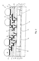
- an electronic component 10 including a base insulative layer 12 having a first surface 14 and a second surface 16.
- An electronic device 18 secures to the base insulative layer.
- the electronic device has a first surface 20 and a second surface 22.
- At least one I/O contact 24 is located on the first surface of the electronic device.
- a frame panel 26 includes a first region 28 comprised of a first material and a second region 30 comprised of a second material. The first material and the second material differ from each other.
- a surface of the frame panel first region is secured to the base insulative layer.
- the frame panel also includes at least one aperture, wherein the electronic device is disposed within the aperture.
- the base insulative layer is formed from an electrically insulating material.
- the base insulative layer may be a polymer film to which an electrically conductive material can be secured.
- Suitable material for use as the base insulative layer may include one or more of polyimide, polyetherimide, benzocyclobutene (BCB), liquid crystal polymer, bismaleimide-triazine resin (BT resin), epoxy, or silicone.
- Suitable commercially available materials for use as the base insulative layer may include KAPTON H polyimide or KAPTON E polyimide (manufactured by E. I.
- the base insulative layer is fully cured as KAPTON H polyimide.
- the base insulative layer may be formed into an interconnect structure, flex circuit, circuit board, or other structure.
- the interconnect structure can mount and interconnect with one or more electronic devices.
- selection properties for the base insulative layer include an elastic modulus and coefficients of thermal and humidity expansion that provide minimal dimensional change during processing. To maintain flexibility, the thickness of the base insulative layer may be minimized.
- the base insulative layer must have enough rigidity (due to either thickness, a support structure, or material characteristic) to support layers of metallization optionally on both the first and second surfaces of the base insulative layer.
- suitable thickness may be selected with reference to the end-use application, the number and type of electronic devices, and the like.
- the thickness may be greater than about 10 micrometers.
- the thickness may be less than about 50 micrometers.
- the base insulative layer has a thickness in a range of from about 10 micrometers to about 20 micrometers, from about 20 micrometers to about 30 micrometers, from about 30 micrometers to about 40 micrometers, from about 40 micrometers to about 50 micrometers, or greater than about 50 micrometers.
- the base insulative layer is a circuit board
- its suitable thickness may be based on the number of layers within the circuit board.
- the number of circuit board layers generally ranges from about 2 to about 50 or more with each layer having a thickness of about 100 micrometers.
- the first surface of the electronic device may be the active surface of the device upon which one or more I/O contacts are located.
- I/O contacts which may be located on the electronic device, include pads, pins, bumps, and solder balls.
- the I/O contacts are I/O pads.
- Other suitable electronic devices may be a packaged or unpackaged semiconductor chip such as a microprocessor, a microcontroller, a video processor, or an ASIC (Application Specific Integrated Circuit); a discrete passive; or a ball grid array (BGA) carrier.
- the electronic device is a semiconductor silicon chip with an array of I/O contact pads disposed on its first surface.
- the frame panel has a first surface 32 and a second surface 34.
- the first surface of the electronic device and the first surface of the frame panel secure to the second surface of the base insulative layer.
- the base insulative layer may bond to the frame panel and electronic device using an adhesive layer 36.
- the adhesive layer comprises a thermoset adhesive.
- suitable adhesives may include a thermoset polymer.
- Suitable thermoset polymers may include an epoxy, silicone, acrylate, urethane, polyetherimide, or polyimide.
- thermoset adhesives may include a polyimide such as CIBA GEIGY 412 (manufactured by Ciba Geigy), AMOCO AI-10 (manufactured by Amoco Chemicals Corporation) and PYRE-MI (manufactured by E. I. du Pont de Nemours & Co.).
- CIBA GEIGY 412 has a glass transition temperature of about 360 degrees Celsius.
- Other suitable adhesives may include thermoplastic adhesives, water cure adhesives, air cure adhesives, and radiation cure adhesives.
- the adhesive layer may have a thickness greater than about 5 micrometers. In one embodiment, the adhesive layer has a thickness in a range of from about 5 micrometers to about 10 micrometers, from about 10 micrometers to about 20 micrometers, from about 20 micrometers to about 30 micrometers, from about 30 micrometers to about 40 micrometers, from about 40 micrometers to about 50 micrometers, or greater than about 50 micrometers.
- the frame panel has a surface that defines an aperture or an opening 42 for each electronic device site on the base insulative layer.
- Each opening in the frame panel may be in a range of from about 0.2 millimeters (mm) to about 5 mm larger in the x and y dimensions than the electronic device.
- the frame panel stabilizes the base insulative layer during fabrication of the interconnect structure, and also may increase the planarity of the unencapsulated surface of the base insulative layer during processing.
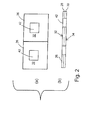
- the frame panel may be a relatively permanent component of the interconnect structure. As shown in Fig. 2(a) , the frame panel may be large enough to comprise a plurality of apertures, wherein each aperture is for a different electronic device site on the base insulative layer, and whereby the frame panel provides stability and increased planarity to a plurality of electronic device sites.
- the frame panel may comprise a single aperture and be sized to provide stability and increased planarity to one electronic device site on the base insulative layer.
- the first region and second region of the frame panel comprise different materials.
- the first region and second region of the frame panel differ in function, and the material selection for the regions is based on that proscribed function.
- the first region is defined by a relatively high affinity or adhesability to the base insulative layer relative to the second region.
- the material selection for the first region then, can be based on the adhesive, the base insulative layer, the method of adhesion, fabrication parameters, and the like.
- the second region has a relatively lower high affinity or adhesability to the base insulative layer than the first region. But, the second region has a relatively higher dimensional stability, or resistance to stress, temperature or humidity.
- the material selection for the second region can be based on process conditions, use conditions, and other considerations.
- the first region of the frame panel may include a material that facilitates bonding of the frame panel to the base insulative layer, as illustrated in Fig. 1 .
- the first region may be a polymeric material.
- Suitable inorganic materials may include a ceramic, a glass, an oxide or a nitride.
- Suitable polymeric materials may include a polyimide, an epoxy, an epoxy blend or a combination of two or more thereof.
- the first region comprises a polymide.
- the polymeric material may include one or more reinforcing fillers. Such fillers may include fibers or small inorganic particles. Suitable fibers may be glass fibers or carbon fibers.
- Suitable particles may include silicon carbide, boron nitride, or aluminum nitride.
- the first region may be an inorganic material. Additives and surface treatments (to both the frame panel and the base insulative layer) may be used to affect and control the adhesive interaction between the frame panel first region and the base insulative layer.
- the second region of the frame panel comprises a material that, in one embodiment, may add strength and durability to the frame panel.
- the second region material may enable the frame panel to have a desirable coefficient of thermal expansion, rigidity, modulus, or thermal conductivity.
- Suitable materials in the second region may include metal or ceramic.
- the second region comprises a metal selected from titanium, iron, copper, tin or a combination of two or more thereof.
- the metal may be an alloy or metal composite, such as stainless steel or Cu:Invar:Cu.
- the second region comprises copper.
- the specific combination of materials the frame panel regions are formed from may be selected for a particular design based on the desired coefficient of thermal expansion, modulus, thermal conductivity, rigidity, surface adhesion, or other desired mechanical properties of the frame panel.
- the frame panel may have a coefficient of thermal expansion (CTE) that is greater than about 3 ppm/°C.
- the frame panel may have a coefficient of thermal expansion (CTE) that is less than about 20 ppm/°C.
- the frame panel may have a thickness equal or close to the thickness of the electronic device.
- the first region and the second region of the frame panel are each in the form of a layer, wherein the two layers are bonded together (see Figs. 1 and 2(b) ).
- the frame panel may be comprised of more than two layers.
- the additional layer(s) may be comprised of material that is similar or different than the material the first and second region layers are comprised of.
- the second region is a layer and the first region is in the form of a partial or full coating over the layer.
- the second region is a layer and the first region comprises a plurality of segments located on a surface of the second region.
- the first region may be comprised of a plurality of segments located within the second region layer, wherein the surface of one or more of the segments is exposed on the first surface of the frame panel.
- the first region is in the form of a layer, and the second region comprises a plurality of segments located on or within the first region layer.
- a surface of the first region segment is in contact with the base insulative layer to provide adhesion.
- a surface of the first region may be exposed on the first surface of the frame panel so that the first region surface can bond to the base insulative layer.
- the surface of the first region may be altered mechanically, chemically or physically to further enhance and improve its capacity for adhesion to the base insulative layer.
- a suitable thickness of the frame panel may be selected with reference to the end-use application, the desired degree of rigidity, the number and type of electronic devices, and the like.
- the thickness may be greater than about 2 micrometers.
- the thickness of the frame panel may be less than about 50 micrometers.
- the frame panel has a thickness in a range of from about 50 micrometers to about 100 micrometers, from about 100 micrometers to about 200 micrometers, from about 200 micrometers to about 400 micrometers, from about 400 micrometers to about 800 micrometers, or greater than about 800 micrometers.
- the thickness of the first or second region layer may be greater than about 0.1 micrometers.
- the thickness may be less than about 100 micrometers.
- the layer has a thickness in a range of from about 0.1 micrometers to about 1.0 micrometers, from about 1.0 micrometers to about 10 micrometers, from about 10 micrometers to about 100 micrometers, or greater than about 100 micrometers.
- an electrical connection between the electronic device and the base insulative layer, as shown in Fig. 1 .
- an electrical connection exists between the I/O contact(s) located on the electronic device and the electrical conductor(s) 44 located on the base insulative layer.
- suitable electrical conductors that may be located on the base insulative layer include pads, pins, bumps, and solder balls.
- the electrical connection between the base insulative layer and the electronic device may be a structure selected based on application specific parameters. For example, an electrically connective pathway may be formed from a solder ball.
- electrical connections include apertures, holes, or vias 46 which may pass through the base insulative layer and the adhesive layer to one or more I/O contacts on the electronic device.
- the vias may be sized so that they are micro-vias.
- traces, power planes or ground planes may be located on the first surface of the base insulative layer.
- Electrically conductive material may be disposed in the vias extending to the I/O contacts on the electronic device and onto the first surface of the base insulative layer.
- the electrically conductive material may be a metal or an electrically conductive polymer.
- suitable electrically conductive materials may include an epoxy, polysulfone, or polyurethane that incorporates metal particle fillers. Suitable metal particles include silver and gold.
- Other suitable metals may include Al, Cu, Ni, Sn, and Ti. Rather than filled polymeric material, inherently conductive polymers may be used.
- Suitable conductive polymers include polyacetylene, polypyrrole, polythiophene, polyaniline, polyfluorene, poly-3-hexylthiophene, polynaphthalenes, poly-p-phenylene sulfide, and poly-p-phenylene vinylene. If viscosity and stability issues are addressed, the inherently conductive polymer may be filled with an electrically conductive filler to further enhance the electrical conductivity. If the electrically conductive material is metal, the electrically conductive material may be present in a metallization pattern on the first surface of the base insulative layer and on the exposed surface of the vias extending to the I/O contacts on the electronic device (see Fig. 1 ).
- Interconnection to one or more complex electronic devices may require an additional interconnection layer to fully route out all of the required chip I/O contacts.
- one or more additional interconnect layers may exist over the first surface of the base insulative layer.
- multiple interconnect layers cooperate to form an interconnect assembly 50.
- Each additional interconnection layer comprises an additional insulative layer 52, having a first surface 54 and a second surface 56.
- Each additional interconnect layer is bonded to a preceding interconnect layer via an adhesive layer 58.
- an additional insulative layer 52 is bonded to the first surface of the base insulative layer.
- Suitable adhesives for use in various embodiments of the invention include those materials indicated as being suitable adhesive materials hereinabove.
- the additional insulative layer 52 may be a self-bonding polymer that bonds directly to the top surface of the preceding interconnect layer. Suitable self-bonding polymers include epoxies. Additionally, the additional insulative layer may be a polymer applied in liquid form and cured in place, thus bonding directly to the preceding interconnect layer. Suitable materials for use as in the self-bonding additional insulative layer may include one or more of polyimide, polyetherimide, benzocyclobutene (BCB), liquid crystal polymer, bismaleimide-triazine resin (BT resin), epoxy, or silicone.
- BCB benzocyclobutene
- BT resin bismaleimide-triazine resin
- silicone silicone
- the electrical conductor(s) 44 on the additional insulative layer is electrically connected to the electrical conductor(s) on a preceding insulative layer.
- vias may extend through an additional insulative layer and through the adhesive layer 58 to selected electrical conductors on the base insulative layer, as shown in Fig. 3 .
- Electrically conductive material as described above, may be disposed in the vias extending to the electrical conductors on the base insulative layer and onto the first surface of the additional insulative layer.
- the electrically conductive material is present in a metallization pattern on the additional insulative layer, as described hereinabove for the first interconnect layer.
- the interconnect assembly has a first surface 62 and a second surface 64.
- a dielectric or solder masking material 68 may be disposed on the first surface of the interconnect assembly to passivate any metal traces and to define contact pads used for assembly or package I/O contacts (see Figs. 1 and 3 ).
- the package I/O contacts may have additional metal depositions such as Ti:Ni:Au applied to the exposed contact pads to provide more robust I/O contacts.
- the I/O contact pads can have pins, solder spheres, or leads attached to them or left as is creating a pad array.
- Fig. 3 depicts an interconnect assembly with an array of solder spheres 69 such as for a ball grid array.
- Other interconnect structures may also be used.
- an interconnect assembly may have an array of pins such as for a pin grid array.
- encapsulation material 70 may be disposed in the area surrounding the electronic device to protect the electronic device and the interconnect structure from moisture and thermo-mechanical stresses.
- the base insulative layer and exposed electronic device may be encapsulated with encapsulation material to fully embed the base insulative layer and the electronic device.
- the base insulative layer and exposed electronic device may be partially encapsulated to embed the base insulative layer and portions of the electronic device.
- Encapsulation materials that may be used include thermoplastic and thermoset polymers. Suitable aliphatic and aromatic polymers may include polyetherimides, acrylates, polyurethanes, polypropylene, polysulfone, polytetrafluoroethylenes, epoxies, benzocyclobutene (BCB), room temperature vulcanizable (RTV) silicones and urethanes, polyimides, polyetherimides, polycarbonates, silicones, and the like.
- the encapsulation material is a thermoset polymer due to the relatively low cure temperatures available.
- the encapsulation material may include a filler material.
- the type, size and amount of the filler material may be used to tailor various molding material properties, such as thermal conductivity, thermal coefficient-of-expansion, viscosity and moisture uptake.
- these materials may include particles, fibers, screens, mats, or plates of inorganic particles.
- Suitable filler materials may include glass, silica, ceramic, silicon carbide, alumina, aluminum nitride, boron nitride, gallium, or other metals, metal oxide, metal carbides, metal nitrides, or metal silicides.
- Other suitable filler materials may include carbon-based materials.
- a gap or moat region may exist between the inner edges of each frame panel opening, and the outer edge of the electronic device disposed within the opening. This gap may either be left unfilled or may be fully or partially filled with encapsulation material. The gap between the inner edges of the frame panel opening, and the outer edge of the electronic device may be partially filled so that it is between about 10% full and about 90% full.
- a lid/thermal spreader 72 may be bonded to the second surface of the electronic device to provide thermal protection to the electronic device.
- the lid/thermal spreader is bonded with a thermal interface material (TIM) 74.
- TIM thermal interface material
- the lid/thermal spreader may also be bonded to the second surface of the frame panel via an adhesive layer 76.
- the backside of the electronic device may be left exposed to facilitate heat removal during device operation for higher power devices with about 5 watts to about 100 watts or more dissipation.
- compositions, structures and systems having elements corresponding to the elements of the invention recited in the claims are examples of compositions, structures and systems having elements corresponding to the elements of the invention recited in the claims.
- This written description may enable those of ordinary skill in the art to make and use embodiments having alternative elements that likewise correspond to the elements of the invention recited in the claims.
- the scope of the invention thus includes compositions, structures, systems and methods that do not differ from the literal language of the claims, and further includes other structures, systems and methods with insubstantial differences from the literal language of the claims. While only certain features and embodiments have been illustrated and described herein, many modifications and changes may occur to one of ordinary skill in the relevant art. The appended claims cover all such modifications and changes.
Landscapes
- Production Of Multi-Layered Print Wiring Board (AREA)
- Structures Or Materials For Encapsulating Or Coating Semiconductor Devices Or Solid State Devices (AREA)
- Combinations Of Printed Boards (AREA)
- Cooling Or The Like Of Semiconductors Or Solid State Devices (AREA)
Applications Claiming Priority (1)
| Application Number | Priority Date | Filing Date | Title |
|---|---|---|---|
| US12/102,429 US8259454B2 (en) | 2008-04-14 | 2008-04-14 | Interconnect structure including hybrid frame panel |
Publications (2)
| Publication Number | Publication Date |
|---|---|
| EP2110849A2 true EP2110849A2 (de) | 2009-10-21 |
| EP2110849A3 EP2110849A3 (de) | 2012-11-28 |
Family
ID=40810020
Family Applications (1)
| Application Number | Title | Priority Date | Filing Date |
|---|---|---|---|
| EP09157431A Ceased EP2110849A3 (de) | 2008-04-14 | 2009-04-06 | Verbindungsstruktur mit Hybridrahmenplatte |
Country Status (5)
| Country | Link |
|---|---|
| US (1) | US8259454B2 (de) |
| EP (1) | EP2110849A3 (de) |
| JP (2) | JP5731741B2 (de) |
| KR (2) | KR101608427B1 (de) |
| TW (1) | TWI447882B (de) |
Cited By (1)
| Publication number | Priority date | Publication date | Assignee | Title |
|---|---|---|---|---|
| WO2018175099A1 (en) * | 2017-03-20 | 2018-09-27 | Qualcomm Incorporated | Low profile integrated package |
Families Citing this family (6)
| Publication number | Priority date | Publication date | Assignee | Title |
|---|---|---|---|---|
| US20120314390A1 (en) * | 2010-03-03 | 2012-12-13 | Mutual-Tek Industries Co., Ltd. | Multilayer circuit board |
| JP5607447B2 (ja) * | 2010-07-22 | 2014-10-15 | セミコンダクター・コンポーネンツ・インダストリーズ・リミテッド・ライアビリティ・カンパニー | 回路装置 |
| US8623699B2 (en) | 2010-07-26 | 2014-01-07 | General Electric Company | Method of chip package build-up |
| US8872340B2 (en) * | 2012-07-17 | 2014-10-28 | SK Hynix Inc. | Substrate for semiconductor package which can prevent the snapping of a circuit trace despite physical deformation of a semiconductor package and semiconductor package having the same |
| JP6465340B2 (ja) * | 2014-11-05 | 2019-02-06 | 日立化成株式会社 | ケイ素を含む基板を用いた半導体装置の製造方法 |
| US9853011B2 (en) | 2016-03-29 | 2017-12-26 | Advanced Semiconductor Engineering, Inc. | Semiconductor package structure and method for manufacturing the same |
Family Cites Families (41)
| Publication number | Priority date | Publication date | Assignee | Title |
|---|---|---|---|---|
| US3436819A (en) * | 1965-09-22 | 1969-04-08 | Litton Systems Inc | Multilayer laminate |
| US4246595A (en) * | 1977-03-08 | 1981-01-20 | Matsushita Electric Industrial Co., Ltd. | Electronics circuit device and method of making the same |
| US4722914A (en) * | 1984-05-30 | 1988-02-02 | Motorola Inc. | Method of making a high density IC module assembly |
| US4566186A (en) * | 1984-06-29 | 1986-01-28 | Tektronix, Inc. | Multilayer interconnect circuitry using photoimageable dielectric |
| CN1094717C (zh) * | 1995-11-16 | 2002-11-20 | 松下电器产业株式会社 | 印刷电路板的安装体 |
| US5869894A (en) * | 1997-07-18 | 1999-02-09 | Lucent Technologies Inc. | RF IC package |
| SE513352C2 (sv) * | 1998-10-26 | 2000-08-28 | Ericsson Telefon Ab L M | Kretskort och förfarande för framställning av kretskortet |
| US6734534B1 (en) * | 2000-08-16 | 2004-05-11 | Intel Corporation | Microelectronic substrate with integrated devices |
| US6586822B1 (en) * | 2000-09-08 | 2003-07-01 | Intel Corporation | Integrated core microelectronic package |
| US6894399B2 (en) * | 2001-04-30 | 2005-05-17 | Intel Corporation | Microelectronic device having signal distribution functionality on an interfacial layer thereof |
| KR100394809B1 (ko) * | 2001-08-09 | 2003-08-14 | 삼성전자주식회사 | 반도체 패키지 및 그 제조 방법 |
| US7183658B2 (en) * | 2001-09-05 | 2007-02-27 | Intel Corporation | Low cost microelectronic circuit package |
| FI119215B (fi) * | 2002-01-31 | 2008-08-29 | Imbera Electronics Oy | Menetelmä komponentin upottamiseksi alustaan ja elektroniikkamoduuli |
| FI115285B (fi) * | 2002-01-31 | 2005-03-31 | Imbera Electronics Oy | Menetelmä komponentin upottamiseksi alustaan ja kontaktin muodostamiseksi |
| JP2003282774A (ja) * | 2002-03-25 | 2003-10-03 | Kyocera Corp | 配線基板およびその製造方法 |
| US6838776B2 (en) * | 2003-04-18 | 2005-01-04 | Freescale Semiconductor, Inc. | Circuit device with at least partial packaging and method for forming |
| US6864165B1 (en) * | 2003-09-15 | 2005-03-08 | International Business Machines Corporation | Method of fabricating integrated electronic chip with an interconnect device |
| FI20031341L (fi) | 2003-09-18 | 2005-03-19 | Imbera Electronics Oy | Menetelmä elektroniikkamoduulin valmistamiseksi |
| JP2005158770A (ja) * | 2003-11-20 | 2005-06-16 | Matsushita Electric Ind Co Ltd | 積層基板とその製造方法及び前記積層基板を用いたモジュールの製造方法とその製造装置 |
| JP4639600B2 (ja) * | 2004-02-04 | 2011-02-23 | 凸版印刷株式会社 | 半導体パッケージ |
| TWI236122B (en) * | 2004-02-27 | 2005-07-11 | Via Tech Inc | A low thermal expansion build-up layer packaging and a method to package a die using the same |
| US6974724B2 (en) * | 2004-04-28 | 2005-12-13 | Nokia Corporation | Shielded laminated structure with embedded chips |
| TWI237883B (en) * | 2004-05-11 | 2005-08-11 | Via Tech Inc | Chip embedded package structure and process thereof |
| FI117812B (fi) | 2004-08-05 | 2007-02-28 | Imbera Electronics Oy | Komponentin sisältävän kerroksen valmistaminen |
| JP4528062B2 (ja) * | 2004-08-25 | 2010-08-18 | 富士通株式会社 | 半導体装置およびその製造方法 |
| TWI264094B (en) * | 2005-02-22 | 2006-10-11 | Phoenix Prec Technology Corp | Package structure with chip embedded in substrate |
| TWI286807B (en) * | 2005-04-26 | 2007-09-11 | Phoenix Prec Technology Corp | Carrying structure of electronic component |
| US7829386B2 (en) * | 2005-08-17 | 2010-11-09 | General Electric Company | Power semiconductor packaging method and structure |
| US20070212813A1 (en) * | 2006-03-10 | 2007-09-13 | Fay Owen R | Perforated embedded plane package and method |
| US8049338B2 (en) * | 2006-04-07 | 2011-11-01 | General Electric Company | Power semiconductor module and fabrication method |
| WO2008035214A2 (en) | 2006-06-21 | 2008-03-27 | W.S. Tylinter | Screen assembly for separating material according to particle size |
| JP2008010705A (ja) * | 2006-06-30 | 2008-01-17 | Phoenix Precision Technology Corp | チップ埋め込み基板のパッケージ構造 |
| TWI308382B (en) * | 2006-07-25 | 2009-04-01 | Phoenix Prec Technology Corp | Package structure having a chip embedded therein and method fabricating the same |
| US7830004B2 (en) * | 2006-10-27 | 2010-11-09 | Taiwan Semiconductor Manufacturing Company, Ltd. | Packaging with base layers comprising alloy 42 |
| TWI352406B (en) * | 2006-11-16 | 2011-11-11 | Nan Ya Printed Circuit Board Corp | Embedded chip package with improved heat dissipati |
| TWI327363B (en) * | 2006-11-17 | 2010-07-11 | Unimicron Technology Corp | Carrier structure for semiconductor chip and method for manufacturing the same |
| TWI366896B (en) * | 2006-11-30 | 2012-06-21 | Carrier structure embedded with chip and method for fabricating thereof | |
| US7598610B2 (en) * | 2007-01-04 | 2009-10-06 | Phoenix Precision Technology Corporation | Plate structure having chip embedded therein and the manufacturing method of the same |
| TWI452661B (zh) * | 2007-01-30 | 2014-09-11 | 全懋精密科技股份有限公司 | 線路直接連接晶片之封裝結構 |
| US20080318413A1 (en) * | 2007-06-21 | 2008-12-25 | General Electric Company | Method for making an interconnect structure and interconnect component recovery process |
| US20090028491A1 (en) * | 2007-07-26 | 2009-01-29 | General Electric Company | Interconnect structure |
-
2008
- 2008-04-14 US US12/102,429 patent/US8259454B2/en active Active
-
2009
- 2009-04-01 TW TW098110923A patent/TWI447882B/zh active
- 2009-04-06 EP EP09157431A patent/EP2110849A3/de not_active Ceased
- 2009-04-09 JP JP2009094668A patent/JP5731741B2/ja active Active
- 2009-04-13 KR KR1020090031703A patent/KR101608427B1/ko active Active
-
2014
- 2014-07-09 JP JP2014141109A patent/JP2014187406A/ja active Pending
-
2016
- 2016-03-28 KR KR1020160036904A patent/KR101697045B1/ko active Active
Non-Patent Citations (1)
| Title |
|---|
| None * |
Cited By (2)
| Publication number | Priority date | Publication date | Assignee | Title |
|---|---|---|---|---|
| WO2018175099A1 (en) * | 2017-03-20 | 2018-09-27 | Qualcomm Incorporated | Low profile integrated package |
| US10651160B2 (en) | 2017-03-20 | 2020-05-12 | Qualcomm Incorporated | Low profile integrated package |
Also Published As
| Publication number | Publication date |
|---|---|
| JP5731741B2 (ja) | 2015-06-10 |
| KR101608427B1 (ko) | 2016-04-01 |
| JP2014187406A (ja) | 2014-10-02 |
| JP2009260347A (ja) | 2009-11-05 |
| EP2110849A3 (de) | 2012-11-28 |
| US8259454B2 (en) | 2012-09-04 |
| KR101697045B1 (ko) | 2017-01-16 |
| KR20090109062A (ko) | 2009-10-19 |
| US20090255709A1 (en) | 2009-10-15 |
| TWI447882B (zh) | 2014-08-01 |
| KR20160040161A (ko) | 2016-04-12 |
| TW201001661A (en) | 2010-01-01 |
Similar Documents
| Publication | Publication Date | Title |
|---|---|---|
| TWI628750B (zh) | 功率覆蓋結構及其製造方法 | |
| TWI613774B (zh) | 功率覆蓋結構及其製造方法 | |
| KR101697045B1 (ko) | 혼성 프레임 패널을 포함하는 상호접속 구조물 | |
| US9806051B2 (en) | Ultra-thin embedded semiconductor device package and method of manufacturing thereof | |
| US9070568B2 (en) | Chip package with embedded passive component | |
| US7005320B2 (en) | Method for manufacturing flip chip package devices with a heat spreader | |
| JP2001291801A (ja) | 直接取付けチップスケール・パッケージ | |
| KR20090062612A (ko) | 멀티 칩 패키지 | |
| US6992380B2 (en) | Package for semiconductor device having a device-supporting polymeric material covering a solder ball array area | |
| US20050133929A1 (en) | Flexible package with rigid substrate segments for high density integrated circuit systems | |
| KR100836642B1 (ko) | 전자 패키지 및 그 제조방법 | |
| KR100836657B1 (ko) | 전자 패키지 및 그 제조방법 | |
| JP2000058716A (ja) | 半導体装置 |
Legal Events
| Date | Code | Title | Description |
|---|---|---|---|
| PUAI | Public reference made under article 153(3) epc to a published international application that has entered the european phase |
Free format text: ORIGINAL CODE: 0009012 |
|
| AK | Designated contracting states |
Kind code of ref document: A2 Designated state(s): AT BE BG CH CY CZ DE DK EE ES FI FR GB GR HR HU IE IS IT LI LT LU LV MC MK MT NL NO PL PT RO SE SI SK TR |
|
| PUAL | Search report despatched |
Free format text: ORIGINAL CODE: 0009013 |
|
| AK | Designated contracting states |
Kind code of ref document: A3 Designated state(s): AT BE BG CH CY CZ DE DK EE ES FI FR GB GR HR HU IE IS IT LI LT LU LV MC MK MT NL NO PL PT RO SE SI SK TR |
|
| AX | Request for extension of the european patent |
Extension state: AL BA RS |
|
| RIC1 | Information provided on ipc code assigned before grant |
Ipc: H01L 21/60 20060101AFI20121019BHEP Ipc: H01L 23/538 20060101ALI20121019BHEP |
|
| 17P | Request for examination filed |
Effective date: 20130528 |
|
| RBV | Designated contracting states (corrected) |
Designated state(s): AT BE BG CH CY CZ DE DK EE ES FI FR GB GR HR HU IE IS IT LI LT LU LV MC MK MT NL NO PL PT RO SE SI SK TR |
|
| 17Q | First examination report despatched |
Effective date: 20160901 |
|
| STAA | Information on the status of an ep patent application or granted ep patent |
Free format text: STATUS: THE APPLICATION HAS BEEN REFUSED |
|
| 18R | Application refused |
Effective date: 20191121 |