EP2110850A2 - Dispositif pour mettre deux tranches de semi-conducteur en contact mutuel - Google Patents
Dispositif pour mettre deux tranches de semi-conducteur en contact mutuel Download PDFInfo
- Publication number
- EP2110850A2 EP2110850A2 EP09008647A EP09008647A EP2110850A2 EP 2110850 A2 EP2110850 A2 EP 2110850A2 EP 09008647 A EP09008647 A EP 09008647A EP 09008647 A EP09008647 A EP 09008647A EP 2110850 A2 EP2110850 A2 EP 2110850A2
- Authority
- EP
- European Patent Office
- Prior art keywords
- contact
- diode laser
- wafer
- arrangement
- diode
- Prior art date
- Legal status (The legal status is an assumption and is not a legal conclusion. Google has not performed a legal analysis and makes no representation as to the accuracy of the status listed.)
- Granted
Links
Images


Classifications
-
- H—ELECTRICITY
- H10—SEMICONDUCTOR DEVICES; ELECTRIC SOLID-STATE DEVICES NOT OTHERWISE PROVIDED FOR
- H10W—GENERIC PACKAGES, INTERCONNECTIONS, CONNECTORS OR OTHER CONSTRUCTIONAL DETAILS OF DEVICES COVERED BY CLASS H10
- H10W76/00—Containers; Fillings or auxiliary members therefor; Seals
- H10W76/60—Seals
-
- H—ELECTRICITY
- H10—SEMICONDUCTOR DEVICES; ELECTRIC SOLID-STATE DEVICES NOT OTHERWISE PROVIDED FOR
- H10W—GENERIC PACKAGES, INTERCONNECTIONS, CONNECTORS OR OTHER CONSTRUCTIONAL DETAILS OF DEVICES COVERED BY CLASS H10
- H10W90/00—Package configurations
-
- H—ELECTRICITY
- H10—SEMICONDUCTOR DEVICES; ELECTRIC SOLID-STATE DEVICES NOT OTHERWISE PROVIDED FOR
- H10W—GENERIC PACKAGES, INTERCONNECTIONS, CONNECTORS OR OTHER CONSTRUCTIONAL DETAILS OF DEVICES COVERED BY CLASS H10
- H10W95/00—Packaging processes not covered by the other groups of this subclass
-
- H—ELECTRICITY
- H10—SEMICONDUCTOR DEVICES; ELECTRIC SOLID-STATE DEVICES NOT OTHERWISE PROVIDED FOR
- H10W—GENERIC PACKAGES, INTERCONNECTIONS, CONNECTORS OR OTHER CONSTRUCTIONAL DETAILS OF DEVICES COVERED BY CLASS H10
- H10W72/00—Interconnections or connectors in packages
- H10W72/071—Connecting or disconnecting
- H10W72/072—Connecting or disconnecting of bump connectors
- H10W72/07251—Connecting or disconnecting of bump connectors characterised by changes in properties of the bump connectors during connecting
-
- H—ELECTRICITY
- H10—SEMICONDUCTOR DEVICES; ELECTRIC SOLID-STATE DEVICES NOT OTHERWISE PROVIDED FOR
- H10W—GENERIC PACKAGES, INTERCONNECTIONS, CONNECTORS OR OTHER CONSTRUCTIONAL DETAILS OF DEVICES COVERED BY CLASS H10
- H10W72/00—Interconnections or connectors in packages
- H10W72/20—Bump connectors, e.g. solder bumps or copper pillars; Dummy bumps; Thermal bumps
-
- H—ELECTRICITY
- H10—SEMICONDUCTOR DEVICES; ELECTRIC SOLID-STATE DEVICES NOT OTHERWISE PROVIDED FOR
- H10W—GENERIC PACKAGES, INTERCONNECTIONS, CONNECTORS OR OTHER CONSTRUCTIONAL DETAILS OF DEVICES COVERED BY CLASS H10
- H10W72/00—Interconnections or connectors in packages
- H10W72/90—Bond pads, in general
- H10W72/921—Structures or relative sizes of bond pads
- H10W72/922—Bond pads being integral with underlying chip-level interconnections
- H10W72/9226—Bond pads being integral with underlying chip-level interconnections with via interconnections
-
- H—ELECTRICITY
- H10—SEMICONDUCTOR DEVICES; ELECTRIC SOLID-STATE DEVICES NOT OTHERWISE PROVIDED FOR
- H10W—GENERIC PACKAGES, INTERCONNECTIONS, CONNECTORS OR OTHER CONSTRUCTIONAL DETAILS OF DEVICES COVERED BY CLASS H10
- H10W72/00—Interconnections or connectors in packages
- H10W72/90—Bond pads, in general
- H10W72/921—Structures or relative sizes of bond pads
- H10W72/923—Bond pads having multiple stacked layers
Definitions
- the present invention relates to a device for the mutual contacting of two wafer-like component composite arrangements of a plurality of interconnected similar components, in particular a semiconductor wafer with a functional component wafer, for the production of wafer-level electronic assemblies according to claim 1.
- the device of the aforementioned type is generally used when it comes to connect in a composite coherently formed substrates with also arranged in a composite components without previous dissolution of the respective composite together.
- chips or chip modules with the function components controlled via the chips, such as a laser diode, both the chip and the laser diode on the wafer level, ie in a continuous wafer composite, and then before contacting the chip with the laser diode both the chip and the laser diode to separate from the respective wafer composite.
- the present invention is based on the object to enable production of corresponding electronic assemblies on the wafer level and also to ensure that even with temperature-sensitive functional components an allowable temperature load is not exceeded.
- the device according to the invention has the features of claim 1.
- the device according to the invention is provided with a receiving frame for supportingly receiving a first wafer on a transparent plate arranged in the receiving frame and a diode laser composite arrangement arranged separated from the wafer by the transparent plate within the receiving frame. Furthermore, the device according to the invention on a counter-holder for receiving a second wafer, such that the provided with Maismetallmaschineenen Contact surfaces of the wafer are arranged opposite to each other, as well as a positioning device for relative positioning of the wafer, such that form together to be connected contact metallizations contact pairings. In addition, the device according to the invention is provided with a pressure device for generating a contact pressure between the contact metallizations of the contact pairings.
- the diode laser array is implemented as a diode laser linear array having a plurality of serially arranged diode lasers disposed on a diode laser carrier movable transversely to the alignment of the row and parallel to the plane of extent of the wafer.
- the diode lasers of the diode laser linear array can be activated individually or in groups, such that only a diode laser of the diode laser linear array can be activated to act on a circular surface wafer contact surface with the diode laser linear array movable parallel to the plane of extent of the wafer are needed depending on the travel to cover the associated transverse extent of the wafer contact surface.
- the diode laser array is formed as a diode laser array array having a plurality of diode lasers arranged in rows and columns, respectively.
- the diode lasers can be activated individually or in groups such that with a coaxial alignment of the surface centers of the wafer contact surface and the matrix surface the diode lasers correspond to the size of the wafer contact surface in their entirety or only can be activated in the scope of a partial matrix required for covering the wafer contact surface.
- a transmission device is arranged in a space formed by a distance between the transparent plate and the diode laser composite arrangement, which serves for measuring a reference temperature.
- the wafer opposite the wafer subjected to laser radiation at the rear is arranged in an at least biaxially movable positioning device.
- the positioning device is of three-axis design, such that, in addition to a biaxial positioning of the wafer in the plane of extent of the wafer, the positioning device serves to execute a feed movement transversely to the plane of extent, the positioning device can also be used for generating the contact pressure required for producing the contacting.
- the two wafers each provided with contact metallizations on their opposing contact surfaces are brought into a covering position with their contact metallizations in order to form contact pairs, in which the contact metallizations to be connected to one another are pressed against one another.
- the contacting of the contact metallizations is effected by a rear exposure of the one wafer with laser radiation, wherein the wavelength of the laser radiation is selected depending on the degree of absorption of the back-acting wafer so that a transmission of the laser radiation is substantially omitted by the wafer backwardly acted upon.
- the wafer composite created by the contacting of the two wafers can subsequently be dissolved by separation into isolated electronic assemblies consisting of a chip and a functional component contacted therewith.
- the component radiation arrangement acted upon at the rear by laser radiation is selected such that a transmission of the laser radiation takes place through the component composite applied at the rear with laser radiation and absorption of the laser radiation takes place substantially only in the contact metallizations of the component assembly applied rearwardly with laser radiation it is possible for the contacting, which in principle can be done in the process by thermocompression or curing of an adhesive or other possible types of connection, which require a heat input for activation to perform necessary heating of the contact metallizations by a substantially immediate heating of the justifymetallmaschineen.
- the contact metallizations of the component radiation beam arrangement acted upon at the rear by laser radiation are selected from a material which has a higher heat capacity compared to the substrate material of the oppositely arranged component assembly, it can be achieved that the temperature increase required for the contacting is substantially only takes place in the area of contact metallizations.
- a simultaneous introduction of heat into the contact metallizations of the component radiation arrangement acted upon at the rear by laser radiation and the contact metallizations of the oppositely arranged component composite arrangement can take place when the component composite arrangement acted upon at the rear by laser radiation is selected so that a transmission of the laser radiation is effected by the applied rearward with laser radiation component composite assembly and an absorption of the laser radiation in the justifymetallmaschineen the applied rearward with laser radiation component composite assembly and in comparison to the justifymetallmaschineen the rear loaded with laser radiation device Composite arrangement areally larger contact metallizations of the opposite component composite assembly takes place.
- the laser application takes place by means of a composite arrangement of a plurality of diode lasers, which are activated individually or in groups for the emission of laser radiation, such that all or in groups combined contact pairings for contacting with laser radiation are applied.
- the use of laser diodes for laser application of the wafer enables a particularly exact adjustability of the wavelength emitted by the laser-active layer of the diode laser, so that a correspondingly high degree of absorption in the wafer applied to the rear can be achieved.
- the defined activation of selected diode lasers from a composite arrangement enables laser application just to the extent required for contacting. In a corresponding manner, the wafer applied to the rear is only heated as far as is absolutely necessary for contacting. This also reduces a possible heat radiation transition from the first wafer heated up by absorption to the second wafer provided opposite to the contacting.
- the diode laser array is formed as a diode laser linear array spaced below the backside laser beamed wafer, such that the diode laser array is at least uniaxial and parallel to Extension level of the wafer is moved, a relatively small number of diode lasers is sufficient.
- the diode laser array as a diode laser array, wherein the diode lasers are activated in accordance with the size of the wafer to be backlashed with laser radiation in its entirety or only in the periphery of a sub-array. This allows the simultaneous contacting of all contact pairings, so that the contacting at the wafer level with minimum temperature load for the other wafer within a very short time is feasible.
- a reference temperature is measured in a gap formed by the distance between the wafer applied to the rear and the diode laser composite arrangement by means of a transmission device penetrated by the laser radiation, it is possible to continuously monitor the temperature in the backwashed wafer during laser application, for example at Achieving a temperature threshold, the diode laser composite assembly at least temporarily turn off.
- a component composite made from two mutually contacted wafer-like component composite assemblies using the above apparatus includes a first transparent composite component assembly of a plurality of contiguous ones formed transparent cover units and a second component composite assembly of a plurality of coherently formed sensor units, each with at least one sensor, which is contacted in each case on one of the coherently formed composite substrate units, which are provided with through holes for a rear contact access to the sensor unit.
- the above structure of the component assembly allows the production of a total completed sensor chip without an inadmissibly high temperature load of the sensor during the manufacturing process.
- the opposing contact metallizations of the cover units and sensor units to be contacted with one another have a solder material. This makes it possible to carry out the contacting in a thermocompression method.
- At least one group is provided with a conductive adhesive as the contact material of the group of contact metallizations assigned to the cover units and the group of contact metallizations assigned to the sensor units.
- a conductive adhesive as the contact material of the group of contact metallizations assigned to the cover units and the group of contact metallizations assigned to the sensor units.
- the contact material provided for the contacting it proves to be advantageous if at least one group of the contact metallizations as a lower layer for the contact material, so for example, the solder material or the adhesive material, an absorption layer of a highly absorbent material, such as chromium , As a result, irrespective of the degree of transmission of the substrate materials used for the cover units or the sensor units, increased heating in the area of the contact metallizations occurs in the region of the contact metallizations.
- an adhesion promoter layer can be selected from an adhesion material adapted to the particular combination of the material used for the absorption layer and the contact material.
- the absorption layer of the group of contact metallizations assigned to the sensor units has an enlarged surface compared to the absorption layer of the group of contact metallizations assigned to the cover units, targeted heat input can occur not only in the contact metallizations of the cover units but also in the contact metallizations of the sensor units.
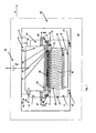
- FIG. 12 shows a wafer contacting apparatus 10 having a pickup frame 11 for supportingly receiving a first wafer formed here as a semiconductor wafer 12 and a backstop 13 having a second wafer held thereon, in the present case as a functional component wafer 14 having a plurality therein formed in composite plastic lens parts is formed.
- the receiving frame 11 consists of a frame cylinder 15 which has at its upper end an annular shoulder 16 which serves to receive a glass plate 17 here as a transparent plate. At its end opposite the glass plate 17 front end of the receiving frame 11 is provided with a diode laser assembly 18. Above the diode laser composite arrangement 18 is a transmission device 19, which allows the laser radiation 20 emitted by the diode laser composite arrangement 18 to pass through substantially without absorption and is provided with at least one temperature sensor device not shown here for measuring a reference temperature. In addition, in the frame cylinder 15 circumferentially a pressure port 21 is provided, which acts on a between the glass plate 17 and the diode laser composite assembly 18 and the Transmission device 19 formed frame interior 40 allows compressed air.
- a frame cylinder 51 having counter-holder 13 has received by the frame cylinder 51 a pressure-resistant housing 22, which is provided with a vacuum port 23.
- a serving as a counter-surface 24 wall of the housing 22 is designed as a porous plate.
- the functional component wafer 14 is when applying a vacuum to the vacuum port 23 against the counter-holding surface 24 in the in Fig. 1 kept illustrated manner.
- the porous plate is provided with a resilient, porous intermediate layer 54 to compensate for local variations in the effective between themaschinemetallmaschineen during contacting contact pressure can.
- process space 25 is circumferentially sealed by an elastic seal 26 from the environment.
- the process space 25 is connected to the environment via gas connections 27, 28.
- the gas connections 27, 28 allow the application of a vacuum or, for example, the admission of the process space 25 with a protective gas.
- a vacuum degassing may prove to be advantageous, for example, when using adhesive material as a connecting material.
- the receiving frame 11 is held together with the anvil 13 in a circumferentially closed machine frame 29.
- the positioning device 31 In addition to the two-axis relative positioning of the housing part 32 relative to the housing part 33 about a perpendicular to the planar extent of the wafer 12, 14 extending Z axis and parallel to the planar extent of the wafer 12, 14 extending X-axis 35 allows the positioning device 31, a relative movement of the housing part 32 to the housing part 33 in the direction of the Z-axis and thus a feed movement of the functional component wafer 14 in the direction of the semiconductor wafer 12 for generating the contact or contact pressure required for the contacting.
- force measuring cells 37 are arranged distributed over the frontal periphery of the receiving frame 11 between the receiving frame 11 and a frame undercarriage 36 of the machine frame.
- the semiconductor wafer 12 is placed on the glass plate 17 of the receiving frame 11.
- the exact relative positioning of Contact metallizations on a contact surface 38 of the functional component wafer 14 to contact metallizations on a contact surface 39 of the semiconductor wafer 12 by forming contact pairings of each associated contact metallizations.
- the alignment required for this purpose takes place by means of the positioning device 31 and corresponding actuation of axis controls about the Z-axis and in the direction of the X-axis.
- the monitoring of the positioning can be done for example via an optical monitoring system, not shown here in detail, in is able to detect an overlap of at least two spaced-apart contact pairings between contact metallizations of the semiconductor wafer 12 and contact metallizations of the functional device wafer 14.
- a delivery of the counter-holder 13 is carried out in the direction of the receiving frame 11 by an axis control of the positioning device 31 in the direction of the Z-axis until detected via the load cells 37 reaching the threshold for the correct contact pressure and the corresponding axis drive off becomes.
- the interior 40 of the receiving frame 11 via the pressure port 41 with a fluid pressure, ie a gas pressure or a liquid pressure, are applied.
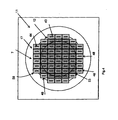
- FIGS. 2 and 3 is a plan view of the receiving frame 11 according to the section line II-II in Fig. 1 shown.
- the semiconductor wafer 12 which is merely shown with regard to its contour contours, and which is arranged on the glass plate 17 of the receiving frame 11 and is acted on at the rear by laser radiation 20 by means of a diode laser linear arrangement 42.
- the diode laser linear array 42 comprises seven arranged on a diode laser carrier 52 laser diodes 43 which emit according to their typical layered formation with a laser active layer each having an approximately rectangular in cross-section beam path 44, which widens to a beam cross-sectional area 45, which regularly up to several Square centimeter, rear impacts on the semiconductor wafer 12 and depending on the pad density of the Semiconductor wafer 12 a larger number of pads simultaneously exposed to laser radiation.
- the diode laser linear arrangement 42 is provided with a drive, which is not described here in greater detail, which makes it possible to activate the diode lasers 43 of the diode laser linear arrangement 42 individually or in groups in a group.
- the diode laser linear array 42 For backward loading of the entire contact surface of the semiconductor wafer 12, the diode laser linear array 42, starting from the in Fig. 2 shown initial position over the entire diameter of the semiconductor wafer 12 method. In each case, only those and so many diode lasers 43 are activated as a function of the travel path 46 in order to be able to cover the respective diameter of the semiconductor wafer 12 transversely to the travel path 46.
- Fig. 4 10 shows a diode laser matrix arrangement 47 with ten diode laser columns 48 and seven diode laser rows 49.
- the matrix of the diode laser matrix array 47 is irregularly formed. to be able to apply laser radiation to the entire contact surface 39 of the semiconductor wafer 12.
- Fig. 4 is illustrated by the cross-hatched representation of a portion of the beam cross-sectional areas 45 of the diode laser 43, it is sufficient for laser exposure of a semiconductor wafer 50 reduced in diameter compared to the semiconductor wafer 50 to activate only a portion of the diode laser 43 corresponding to a sub-array 53.
- Fig. 5 1 shows a section of the area of a sensor chip unit 57 of a sensor chip component composite 58 produced in a component assembly from a cover unit composite arrangement 55 and a sensor unit composite arrangement 56.
- the sensor die component assembly 58 is formed by means of the in Fig. 1 produced wafer contacting device 10 can be produced.
- cover units 59 which are formed in the wafer-like cover unit composite assembly 55 is contiguous.
- the cover units 59 have in the present case a transparent substrate material, such as glass frit, which is optically transparent, and have on their contact surface 60 contact metallizations 61, which in the present case with a solder material as a contact material 62, for example a gold-tin alloy , are provided.
- the contact metallizations 61 have an absorption layer 63, which is designed as a lower layer and faces the laser radiation 20, which, for example, may essentially contain chromium.
- the sensor unit composite assembly 56 is composed of a plurality of interconnected composite, each associated with a cover unit 59 sensor units 64 composed.
- the sensor units 64 have a silicon substrate 65, which is provided with contact metallizations 67 on its inner contact surface 65 facing the cover unit 59.
- the contact metallizations 67 are provided in the present case in accordance with the associated contact metallizations 61 of the cover unit 59 with a solder material as the contact material 68.
- the contact metallizations 67 have absorption layers 69 arranged as a lower layer to the contact material 68, which project peripherally beyond the contact material 68 such that a portion of the through the optically transparent substrate material of the cover unit 59 passes through reached laser radiation 20 in a peripheral projection 70 of the absorption layers 69 is absorbed.
- the inner contact metallizations 67 disposed adjacent to a sensor 71 of the sensor unit 64 are provided with vias 72 through the substrate 65 which enable external contacting via outer contact metallizations 73 on an outer contact surface 74 of the sensor units 64.
- the contact metallizations 67 adjacent to the sensor 71 are electrically contacted to the sensor 71 in a manner not shown here, so that an external direct contact of the sensor 71 via the outer contact metallizations 73 is made possible by means of the plated-through holes 72.
- the substrate material of the cover units 59 can also be designed to be absorbent, since the temperature-sensitive sensor 71 is arranged on the sensor units 64 that are not directly exposed to laser radiation 20.
Landscapes
- Semiconductor Lasers (AREA)
- Container, Conveyance, Adherence, Positioning, Of Wafer (AREA)
- Photo Coupler, Interrupter, Optical-To-Optical Conversion Devices (AREA)
Applications Claiming Priority (3)
| Application Number | Priority Date | Filing Date | Title |
|---|---|---|---|
| DE10357027 | 2003-12-03 | ||
| DE10361521A DE10361521A1 (de) | 2003-12-03 | 2003-12-23 | Verfahren und Vorrichtung zur wechselseitigen Kontaktierung von zwei Wafern |
| EP04802856A EP1697966B1 (fr) | 2003-12-03 | 2004-12-02 | Procede pour mettre deux tranches de semi-conducteur en contact mutuel |
Related Parent Applications (2)
| Application Number | Title | Priority Date | Filing Date |
|---|---|---|---|
| EP04802856.7 Division | 2004-12-02 | ||
| EP04802856A Division EP1697966B1 (fr) | 2003-12-03 | 2004-12-02 | Procede pour mettre deux tranches de semi-conducteur en contact mutuel |
Publications (3)
| Publication Number | Publication Date |
|---|---|
| EP2110850A2 true EP2110850A2 (fr) | 2009-10-21 |
| EP2110850A3 EP2110850A3 (fr) | 2012-04-25 |
| EP2110850B1 EP2110850B1 (fr) | 2015-04-22 |
Family
ID=34638425
Family Applications (1)
| Application Number | Title | Priority Date | Filing Date |
|---|---|---|---|
| EP20090008647 Expired - Lifetime EP2110850B1 (fr) | 2003-12-03 | 2004-12-02 | Dispositif pour mettre deux tranches de semi-conducteur en contact mutuel |
Country Status (3)
| Country | Link |
|---|---|
| US (1) | US8361881B2 (fr) |
| EP (1) | EP2110850B1 (fr) |
| DE (1) | DE10361521A1 (fr) |
Families Citing this family (3)
| Publication number | Priority date | Publication date | Assignee | Title |
|---|---|---|---|---|
| EP3042395B1 (fr) | 2013-09-05 | 2017-03-08 | Koninklijke Philips N.V. | Élément détecteur de rayonnement |
| DE102016210042B3 (de) * | 2016-06-07 | 2017-10-19 | Sauer Gmbh | Werkzeugmaschine zum Auftragsschweißen |
| CN111211477B (zh) * | 2018-11-21 | 2023-07-28 | 深圳市中光工业技术研究院 | 半导体激光器及其制备方法 |
Citations (3)
| Publication number | Priority date | Publication date | Assignee | Title |
|---|---|---|---|---|
| US4963714A (en) | 1988-10-24 | 1990-10-16 | Raytheon Company | Diode laser soldering system |
| DE4234342A1 (de) | 1992-10-12 | 1994-04-14 | Fraunhofer Ges Forschung | Verfahren zur Materialbearbeitung mit Laserstrahlung |
| EP1346949A2 (fr) | 2002-03-06 | 2003-09-24 | Robert Bosch Gmbh | Procédé de liaison de tranches d'une couvercle de type plaquette en Si en utilisant l'énergie laser localisée, dispositif manufacturé par ce procédé, et systeme utilisé dans ce procédé |
Family Cites Families (32)
| Publication number | Priority date | Publication date | Assignee | Title |
|---|---|---|---|---|
| DE2902002A1 (de) * | 1979-01-19 | 1980-07-31 | Gerhard Krause | Dreidimensional integrierte elektronische schaltungen |
| JPS6130059A (ja) | 1984-07-20 | 1986-02-12 | Nec Corp | 半導体装置の製造方法 |
| JPH0429338A (ja) | 1990-05-24 | 1992-01-31 | Nippon Mektron Ltd | Icの搭載用回路基板及びその搭載方法 |
| DE4235549C2 (de) | 1991-10-21 | 1999-12-09 | Rohm Co Ltd | Gerät zum Justieren einer Lichtquelleneinheit |
| ES2106520T3 (es) | 1993-05-19 | 1997-11-01 | Fraunhofer Ges Forschung | Procedimiento que permite el trabajo de materiales por radiacion emitida por diodos. |
| DE4321804A1 (de) * | 1993-06-30 | 1995-01-12 | Ranco Inc | Verfahren zur Herstellung von Kleinbauelementen |
| JPH0737911A (ja) * | 1993-07-19 | 1995-02-07 | Mitsubishi Electric Corp | 半導体素子のダイボンド装置、及びダイボンド方法 |
| US6624433B2 (en) | 1994-02-22 | 2003-09-23 | Nikon Corporation | Method and apparatus for positioning substrate and the like |
| US5500540A (en) * | 1994-04-15 | 1996-03-19 | Photonics Research Incorporated | Wafer scale optoelectronic package |
| DE19646476C2 (de) | 1996-11-11 | 2002-03-14 | Fraunhofer Ges Forschung | Verbindungsstruktur |
| US5858607A (en) | 1996-11-21 | 1999-01-12 | Kodak Polychrome Graphics | Laser-induced material transfer digital lithographic printing plates |
| US6072148A (en) * | 1996-12-10 | 2000-06-06 | Fraunhofer-Gesellschaft Zur Forderung Der Angewandten Forschung E.V. | Device for producing connections between two respective contact elements by means of laser energy |
| DE19749909C2 (de) * | 1996-12-10 | 2000-08-31 | Fraunhofer Ges Forschung | Vorrichtung zum Herstellen von Verbindungen zwischen jeweils zwei Kontaktelementen mittels Laserenergie |
| DE19751487A1 (de) * | 1997-11-20 | 1999-06-02 | Pac Tech Gmbh | Verfahren und Vorrichtung zur thermischen Verbindung von Anschlußflächen zweier Substrate |
| US6062461A (en) * | 1998-06-03 | 2000-05-16 | Delphi Technologies, Inc. | Process for bonding micromachined wafers using solder |
| US6451624B1 (en) | 1998-06-05 | 2002-09-17 | Micron Technology, Inc. | Stackable semiconductor package having conductive layer and insulating layers and method of fabrication |
| US6423613B1 (en) | 1998-11-10 | 2002-07-23 | Micron Technology, Inc. | Low temperature silicon wafer bond process with bulk material bond strength |
| US6376051B1 (en) | 1999-03-10 | 2002-04-23 | Matsushita Electric Industrial Co., Ltd. | Mounting structure for an electronic component and method for producing the same |
| US6521324B1 (en) * | 1999-11-30 | 2003-02-18 | 3M Innovative Properties Company | Thermal transfer of microstructured layers |
| US20020151115A1 (en) * | 2000-09-05 | 2002-10-17 | Sony Corporation | Process for production of thin film, semiconductor thin film, semiconductor device, process for production of semiconductor thin film, and apparatus for production of semiconductor thin film |
| DE60025214T2 (de) * | 2000-10-19 | 2006-08-24 | Agilent Technologies, Inc. (n.d.Ges.d.Staates Delaware), Palo Alto | Mikrodeckelgehäuse auf Scheibenebene |
| JP4461616B2 (ja) * | 2000-12-14 | 2010-05-12 | ソニー株式会社 | 素子の転写方法、素子保持基板の形成方法、及び素子保持基板 |
| US6717254B2 (en) * | 2001-02-22 | 2004-04-06 | Tru-Si Technologies, Inc. | Devices having substrates with opening passing through the substrates and conductors in the openings, and methods of manufacture |
| JP2003077940A (ja) * | 2001-09-06 | 2003-03-14 | Sony Corp | 素子の転写方法及びこれを用いた素子の配列方法、画像表示装置の製造方法 |
| US6844606B2 (en) | 2002-02-04 | 2005-01-18 | Delphi Technologies, Inc. | Surface-mount package for an optical sensing device and method of manufacture |
| JP4411575B2 (ja) * | 2002-04-25 | 2010-02-10 | セイコーエプソン株式会社 | 電子装置の製造装置 |
| TW546794B (en) | 2002-05-17 | 2003-08-11 | Advanced Semiconductor Eng | Multichip wafer-level package and method for manufacturing the same |
| JP3962282B2 (ja) | 2002-05-23 | 2007-08-22 | 松下電器産業株式会社 | 半導体装置の製造方法 |
| US20030224581A1 (en) * | 2002-06-03 | 2003-12-04 | Robert Bosch Gmbh | Flip chip packaging process using laser-induced metal bonding technology, system utilizing the method, and device created by the method |
| US6888233B2 (en) | 2003-03-10 | 2005-05-03 | Honeywell International Inc. | Systems for buried electrical feedthroughs in a glass-silicon MEMS process |
| US7186637B2 (en) | 2003-07-31 | 2007-03-06 | Intel Corporation | Method of bonding semiconductor devices |
| WO2005055288A2 (fr) | 2003-12-03 | 2005-06-16 | Pac Tech - Packaging Technologies Gmbh | Procede et dispositif pour mettre deux tranches de semi-conducteur en contact mutuel |
-
2003
- 2003-12-23 DE DE10361521A patent/DE10361521A1/de not_active Ceased
-
2004
- 2004-12-02 EP EP20090008647 patent/EP2110850B1/fr not_active Expired - Lifetime
-
2011
- 2011-03-29 US US13/075,046 patent/US8361881B2/en not_active Expired - Fee Related
Patent Citations (3)
| Publication number | Priority date | Publication date | Assignee | Title |
|---|---|---|---|---|
| US4963714A (en) | 1988-10-24 | 1990-10-16 | Raytheon Company | Diode laser soldering system |
| DE4234342A1 (de) | 1992-10-12 | 1994-04-14 | Fraunhofer Ges Forschung | Verfahren zur Materialbearbeitung mit Laserstrahlung |
| EP1346949A2 (fr) | 2002-03-06 | 2003-09-24 | Robert Bosch Gmbh | Procédé de liaison de tranches d'une couvercle de type plaquette en Si en utilisant l'énergie laser localisée, dispositif manufacturé par ce procédé, et systeme utilisé dans ce procédé |
Also Published As
| Publication number | Publication date |
|---|---|
| EP2110850A3 (fr) | 2012-04-25 |
| US8361881B2 (en) | 2013-01-29 |
| DE10361521A1 (de) | 2005-07-07 |
| US20110244651A1 (en) | 2011-10-06 |
| EP2110850B1 (fr) | 2015-04-22 |
Similar Documents
| Publication | Publication Date | Title |
|---|---|---|
| EP1032482B1 (fr) | Procede et dispositif destines a la liaison thermique de surfaces d'assemblage de deux substrats | |
| DE69838071T2 (de) | Halbleiterscheibengrosse integrierte optische elemente | |
| DE69705848T2 (de) | Verfahren zum erzielen von mehreren integrierten optischen köpfe | |
| DE69906704T2 (de) | Integriertes optisches gerät zur erzeugung von getrennten strahlen auf einem detektor, und zugehörige verfahren | |
| EP3469629B1 (fr) | Un grand nombre de modules | |
| DE102013011581B4 (de) | Anordnung aus einem Substrat mit mindestens einem optischen Wellenleiter und einer optischen Koppelstelle und aus einem optoelektronischen Bauelement und Verfahren zur Herstellung einer solchen Anordnung | |
| DE102018200845B4 (de) | Montageverfahren für die Herstellung eines Röntgendetektors, Röntgendetektor und Röntgengerät | |
| DE102012213343A1 (de) | Optoelektronisches halbleiterbauteil mit saphir-flip-chip | |
| EP0811667A2 (fr) | Méthode de réalisation de liaisons de surfaces par adhésifs, d'une bonne résistance mécanique | |
| DE10356885A1 (de) | Verfahren zum Gehäusen von Bauelementen und gehäustes Bauelement | |
| DE69734039T2 (de) | Vorrichtung mit zwei mikromechanischen Substraten für ein mikromechanisches System oder Teil eines mikromechanischen Systems und Verfahren zur Zusammensetzung zweier mikromechanischer Substrate | |
| WO2014127934A1 (fr) | Composant optoélectronique et procédé permettant de le fabriquer. | |
| EP1766674B1 (fr) | Procédé et dispositif permettant la mise en contact mutuel de deux plaquettes | |
| WO2020104514A1 (fr) | Unité émettrice de lumière dotée d'au moins une puce vcsel | |
| EP1697966B1 (fr) | Procede pour mettre deux tranches de semi-conducteur en contact mutuel | |
| EP2110850A2 (fr) | Dispositif pour mettre deux tranches de semi-conducteur en contact mutuel | |
| DE102006031047A1 (de) | Halbleitersensor und Herstellungsverfahren dafür | |
| WO2025172045A1 (fr) | Procédé de transfert d'un composant | |
| DE102008053645A1 (de) | Verfahren zum Herstellen von mehreren Halbleiter-Bauelementen | |
| DE102007004253A1 (de) | Verfahren und Vorrichtung zur Korrektur fehlerhafter Solder-Bump-Arrays | |
| EP1464084A1 (fr) | Ensemble photodiode et procede pour la production d'une liaison entre un premier composant semi-conducteur et un deuxieme composant semi-conducteur | |
| EP1532692B1 (fr) | Dispositif de detection pour detecter un rayonnement, tomographe informatique equipe de ce dispositif de detection et procede de realisation correspondant | |
| DE102015016763B3 (de) | Vorrichtung und Verfahren zum Positionieren und Übertragen auf einem Substrat bereitgestellter elektronischer Bauteile | |
| WO1999035690A1 (fr) | Procede pour produire un composant a semi-conducteur et composant a semi-conducteur obtenu a l'aide dudit procede | |
| EP1627425B1 (fr) | Procede de production d'un ensemble de puces et vernis permettant de mettre en oeuvre ce procede |
Legal Events
| Date | Code | Title | Description |
|---|---|---|---|
| PUAI | Public reference made under article 153(3) epc to a published international application that has entered the european phase |
Free format text: ORIGINAL CODE: 0009012 |
|
| 17P | Request for examination filed |
Effective date: 20090722 |
|
| AC | Divisional application: reference to earlier application |
Ref document number: 1697966 Country of ref document: EP Kind code of ref document: P |
|
| AK | Designated contracting states |
Kind code of ref document: A2 Designated state(s): DE GB |
|
| PUAL | Search report despatched |
Free format text: ORIGINAL CODE: 0009013 |
|
| AK | Designated contracting states |
Kind code of ref document: A3 Designated state(s): DE GB |
|
| RIC1 | Information provided on ipc code assigned before grant |
Ipc: H01L 21/98 20060101ALI20120319BHEP Ipc: H01L 23/10 20060101AFI20120319BHEP Ipc: H01L 21/50 20060101ALI20120319BHEP Ipc: H01L 21/60 20060101ALI20120319BHEP Ipc: H01S 5/042 20060101ALI20120319BHEP |
|
| 17Q | First examination report despatched |
Effective date: 20140827 |
|
| GRAP | Despatch of communication of intention to grant a patent |
Free format text: ORIGINAL CODE: EPIDOSNIGR1 |
|
| INTG | Intention to grant announced |
Effective date: 20141125 |
|
| GRAS | Grant fee paid |
Free format text: ORIGINAL CODE: EPIDOSNIGR3 |
|
| GRAA | (expected) grant |
Free format text: ORIGINAL CODE: 0009210 |
|
| AC | Divisional application: reference to earlier application |
Ref document number: 1697966 Country of ref document: EP Kind code of ref document: P |
|
| AK | Designated contracting states |
Kind code of ref document: B1 Designated state(s): DE GB |
|
| REG | Reference to a national code |
Ref country code: GB Ref legal event code: FG4D Free format text: NOT ENGLISH |
|
| REG | Reference to a national code |
Ref country code: DE Ref legal event code: R096 Ref document number: 502004014892 Country of ref document: DE Effective date: 20150603 |
|
| REG | Reference to a national code |
Ref country code: DE Ref legal event code: R097 Ref document number: 502004014892 Country of ref document: DE |
|
| PLBE | No opposition filed within time limit |
Free format text: ORIGINAL CODE: 0009261 |
|
| STAA | Information on the status of an ep patent application or granted ep patent |
Free format text: STATUS: NO OPPOSITION FILED WITHIN TIME LIMIT |
|
| 26N | No opposition filed |
Effective date: 20160125 |
|
| PGFP | Annual fee paid to national office [announced via postgrant information from national office to epo] |
Ref country code: GB Payment date: 20201222 Year of fee payment: 17 |
|
| GBPC | Gb: european patent ceased through non-payment of renewal fee |
Effective date: 20211202 |
|
| PG25 | Lapsed in a contracting state [announced via postgrant information from national office to epo] |
Ref country code: GB Free format text: LAPSE BECAUSE OF NON-PAYMENT OF DUE FEES Effective date: 20211202 |
|
| P01 | Opt-out of the competence of the unified patent court (upc) registered |
Effective date: 20230529 |
|
| PGFP | Annual fee paid to national office [announced via postgrant information from national office to epo] |
Ref country code: DE Payment date: 20240220 Year of fee payment: 20 |
|
| REG | Reference to a national code |
Ref country code: DE Ref legal event code: R071 Ref document number: 502004014892 Country of ref document: DE |