EP2110954A2 - Circuit émetteur, procédé d'émission et d'utilisation - Google Patents
Circuit émetteur, procédé d'émission et d'utilisation Download PDFInfo
- Publication number
- EP2110954A2 EP2110954A2 EP09004816A EP09004816A EP2110954A2 EP 2110954 A2 EP2110954 A2 EP 2110954A2 EP 09004816 A EP09004816 A EP 09004816A EP 09004816 A EP09004816 A EP 09004816A EP 2110954 A2 EP2110954 A2 EP 2110954A2
- Authority
- EP
- European Patent Office
- Prior art keywords
- power amplifier
- gain
- counter
- register
- output
- Prior art date
- Legal status (The legal status is an assumption and is not a legal conclusion. Google has not performed a legal analysis and makes no representation as to the accuracy of the status listed.)
- Granted
Links
Images

Classifications
-
- H—ELECTRICITY
- H03—ELECTRONIC CIRCUITRY
- H03F—AMPLIFIERS
- H03F3/00—Amplifiers with only discharge tubes or only semiconductor devices as amplifying elements
- H03F3/20—Power amplifiers, e.g. Class B amplifiers, Class C amplifiers
- H03F3/24—Power amplifiers, e.g. Class B amplifiers, Class C amplifiers of transmitter output stages
- H03F3/245—Power amplifiers, e.g. Class B amplifiers, Class C amplifiers of transmitter output stages with semiconductor devices only
-
- H—ELECTRICITY
- H03—ELECTRONIC CIRCUITRY
- H03F—AMPLIFIERS
- H03F3/00—Amplifiers with only discharge tubes or only semiconductor devices as amplifying elements
- H03F3/189—High-frequency amplifiers, e.g. radio frequency amplifiers
- H03F3/19—High-frequency amplifiers, e.g. radio frequency amplifiers with semiconductor devices only
-
- H—ELECTRICITY
- H03—ELECTRONIC CIRCUITRY
- H03F—AMPLIFIERS
- H03F3/00—Amplifiers with only discharge tubes or only semiconductor devices as amplifying elements
- H03F3/72—Gated amplifiers, i.e. amplifiers which are rendered operative or inoperative by means of a control signal
-
- H—ELECTRICITY
- H04—ELECTRIC COMMUNICATION TECHNIQUE
- H04B—TRANSMISSION
- H04B1/00—Details of transmission systems, not covered by a single one of groups H04B3/00 - H04B13/00; Details of transmission systems not characterised by the medium used for transmission
- H04B1/02—Transmitters
- H04B1/04—Circuits
-
- H—ELECTRICITY
- H03—ELECTRONIC CIRCUITRY
- H03F—AMPLIFIERS
- H03F2200/00—Indexing scheme relating to amplifiers
- H03F2200/321—Use of a microprocessor in an amplifier circuit or its control circuit
-
- H—ELECTRICITY
- H03—ELECTRONIC CIRCUITRY
- H03F—AMPLIFIERS
- H03F2200/00—Indexing scheme relating to amplifiers
- H03F2200/366—Multiple MOSFETs are coupled in parallel
-
- H—ELECTRICITY
- H03—ELECTRONIC CIRCUITRY
- H03F—AMPLIFIERS
- H03F2203/00—Indexing scheme relating to amplifiers with only discharge tubes or only semiconductor devices as amplifying elements covered by H03F3/00
- H03F2203/72—Indexing scheme relating to gated amplifiers, i.e. amplifiers which are rendered operative or inoperative by means of a control signal
- H03F2203/7231—Indexing scheme relating to gated amplifiers, i.e. amplifiers which are rendered operative or inoperative by means of a control signal the gated amplifier being switched on or off by putting into cascade or not, by choosing between amplifiers by one or more switch(es)
-
- H—ELECTRICITY
- H03—ELECTRONIC CIRCUITRY
- H03F—AMPLIFIERS
- H03F2203/00—Indexing scheme relating to amplifiers with only discharge tubes or only semiconductor devices as amplifying elements covered by H03F3/00
- H03F2203/72—Indexing scheme relating to gated amplifiers, i.e. amplifiers which are rendered operative or inoperative by means of a control signal
- H03F2203/7236—Indexing scheme relating to gated amplifiers, i.e. amplifiers which are rendered operative or inoperative by means of a control signal the gated amplifier being switched on or off by putting into parallel or not, by choosing between amplifiers by (a ) switch(es)
Definitions
- the present invention relates to a transmission circuit of a radio network, a method of transmitting a signal, and a use.
- Radio network transmission circuits enable the transmission of data via an antenna of a node of the radio network. To set the transmission range, the transmission power of the node is adjustable. Examples of radio networks are described, for example, in the industry standards IEEE 802.11, IEEE 802.15.1 or IEEE 802.15.4.
- the invention has for its object to provide a possible improved method for transmitting.
- a method of transmitting in a radio network is provided.
- a power amplifier is connectable to an antenna.
- the power amplifier is controlled with a count associated with a minimum gain of the power amplifier.
- a count value can be applied as bit value to an x-bit-wide control input.
- the gain is incremented by counting until the count corresponds to a register value stored in a register.
- a clock signal is applied to a binary counter.
- To increase the gain of the power amplifier either count up or count down according to the design of the counter and the power amplifier configuration.
- the transmission signal is generated, for example, by a specific modulation as a function of the data.
- the gain is gradually reduced by counting until the count associated with the smallest gain of the power amplifier is reached.
- To reduce the gain of the power amplifier is counted down or counted up according to the configuration of the counter and the structure of the power amplifier. For example, counting down is done when the smallest gain is assigned the count 0000, for example. For example, it counts up if the smallest gain, for example, the count 1111 is assigned.
- the invention is further based on the object to improve a transmission circuit as possible.
- the transmission circuit has a power amplifier which can be connected to an antenna.
- the transmission circuit for the connection a power output.
- the transmission circuit has a counter whose output is connected to a control input of the power amplifier for outputting a count value for controlling the gain of the power amplifier.
- the output of the counter and the control input of the power amplifier preferably have a corresponding bit width of, for example, four bits.
- the power amplifier has a signal input and is designed to amplify a signal applied to the signal input to be amplified in response to a control signal at the control input.
- the transmission circuit has a register for storing a register value.
- the register has at least one bit width that is greater than or equal to the bit width of the output of the counter.
- the transmitting circuit has a comparator whose inputs are connected to the output of the counter and the register for comparing the register value with the count value.
- the transmission circuit has a control circuit whose input is connected to the comparator and whose output is connected to the counter for controlling a counting operation in dependence on the comparison result of the comparator.
- the transmission circuit is designed and configured to carry out the method explained above.
- the invention is further based on the object of specifying a use.
- the counter, register and comparator are used to step up a gain of a power amplifier of a radio network before sending data from a minimum gain by counting by the counter until a count of the counter reaches a register value stored in the register and to stepwise decrease the Amplification of the power amplifier after sending the data by counting by means of the counter until a count of the smallest gain of the power amplifier is reached.
- the transmission circuit is preferably designed and set up for carrying out the method steps.
- a signal input of the power amplifier is connected to an output of a driver.
- attenuation is continuously reduced to connect the signal input of the power amplifier to the output of the driver.
- the transmission circuit has a controllable attenuator, which is designed for connection, in particular for continuous damping.
- a signal input of the power amplifier is connected via a controllable attenuator to an output of a driver.
- the attenuator has a controllable resistance.
- the attenuator has a field effect transistor.
- the attenuator is designed to continuously change an attenuation and connected to control the attenuation with the control circuit.
- control circuit is set up to control a counting direction and connected to the counter for controlling the counting direction.
- the register is designed and connected in such a way that the register value can be programmed.
- the transmission circuit has a connection to the register, advantageously an interface.
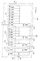
- Fig. 1 shows a schematic block diagram of a transmission circuit of a node of a radio network.
- the transmission circuit comprises a power amplifier (PA - engl P ower A mplifier.) 100, its power output 105 is connected to an output 10 of the transmission circuit.
- PA - engl P ower A mplifier. power amplifier
- its power output 105 is connected to an output 10 of the transmission circuit.
- an antenna 1 At the output 10 of the transmission circuit, which may be formed, for example, as a pad, an antenna 1 can be connected. In this case, the antenna 1 is not necessarily part of the transmission circuit.
- the power amplifier 100 is designed to amplify the signal to be transmitted. To set the gain, the power amplifier has a plurality of controllable sub-amplifiers 110, 120, 130, 140 with associated control lines 101, 102, 103 and 104, respectively.
- the controllable sub-amplifiers 110, 120, 130, 140 are designed, for example, for a linear step-shaped gain setting. Alternatively, a non-linear, for example, logarithmic gain adjustment can be provided.
- the power amplifier 100 also has a further control input 107 for switching on or switching off the amplification of the power amplifier 100.
- a signal input 106 of the power amplifier 100 is connected via a controllable attenuator 700 to the output 602 of a switchable driver (BUF) 600.
- the input of the driver 600 is connected to a modulator 800, which in the embodiment of the Fig. 1 is designed as a PLL (English: P ise L ocked L oop).
- PLL Korean: P ise L ocked L oop
- data D are modulated by the modulator 800 and arrive as a modulated signal to be transmitted via the driver 600 and via the attenuation element 700 set to the lowest attenuation to the input 106 of the power amplifier 100. are amplified in the power amplifier 100 and output to the antenna 1.
- the transmission circuit of the embodiment of Fig. 1 has a counter (CT) 200 whose output lines 211, 212, 213, 214 are connected to the control lines 101, 102, 103 and 104 of the power amplifier 100, respectively.
- a clock signal clk is applied to a clock input of the counter 200.
- the output lines 211, 212, 213, 214 are connected to input lines 311, 312, 313, 314 of a comparator (CP) 300.
- Further input lines 321, 322, 323, 324 of the comparator 300 are connected to output lines 411, 412, 413, 414 of a register (REG) 400.
- the comparator 300 is designed to compare a count value n of the counter 300 with a register value reg of the register 400.
- the count value n has a bit width of four bits n1, n2, n3 and n4.
- the register has a bit width of four bits reg1, reg2, reg3 and reg4.
- the comparison result is output at the output 301 of the comparator 300 and reaches an input 501 of a control circuit 500 connected to the output 301.
- the outputs 502, 503 and 504 of the control circuit 500 are connected to the counter 200 for controlling the counter 200.
- the control circuit 500 may issue a reset signal r to reset the counter 200.
- the control circuit 500 may output an enable signal to start or stop a counter operation of the counter 200.
- the control circuit 500 may output an up-down ud to set a counting direction of the counter 200.
- the control circuit 500 has the output 505 for turning on and off the gain of the power amplifier 100 by means of the control signal S PA , which is connected to a control input 107 of the power amplifier 100.
- control circuit 500 has the output 506 for outputting the control voltage Us, which is connected to a control input (gate) of the damping element 700 designed as an NMOS field-effect transistor for setting the attenuation. Furthermore, the control circuit 500 has the output 507 for turning on and off the driver 600 by means of the control signal S BUF , which is connected to a control input of the driver 600.
- the transmission circuit has in the embodiment of Fig. 1 one or more interfaces to a computing unit, such as a microcontroller core 900 on.
- the transmission circuit can be programmed via the interface / input 401 of the register 400 in that the register value reg can be written to the register 400 via the interface 401.
- a required gain can first be determined by measuring a field strength received in a receiving node. Subsequently, a register value reg corresponding to the required gain is stored in the register 400.
- FIG Fig. 2 An embodiment variant of a power amplifier 100 is shown as a schematic circuit diagram in FIG Fig. 2 shown. All of the gain serving transistors 109, 111, 121, 122, 131, 132, 133, 134, 141, 142, 143, 144, 145, 146, 147 and 148 are connected to the signal input 106 and the power output 105 of the power amplifier 100. The lowest gain is determined by the transistor 109.
- the sub-amplifier 110 is associated with the transistor 111, whose source is connected via the control transistor 119 to ground GND.
- the sub-amplifier 120 has two transistors 121 and 122 for amplification, whose respective source can be connected via the control transistor 129 to ground GND.
- the sub-amplifier 130 has four transistors 131 to 134 for amplification, whose respective source can be connected via the control transistor 139 to ground GND.
- the sub-amplifier 140 has eight transistors 141 and 148 for amplification, their respective source via the Control transistor 149 to ground GND is connectable.
- the respective contributing to the gain transistors 109 to 148 are connected in parallel to each other and act on the same load 150.
- the load 150 is preferably designed as an inductance. Alternatively, the load 150 may be formed as a passive or active resistor or as a power source. By the number of transistors per sub-amplifier, a binary weighting is achieved.
- the control inputs of the control transistors 119 to 149 are connected to the control lines 101 to 104, respectively.
- the power output 105 is connected via the load 150 to a positive supply voltage terminal V +.
- the signal input 106 may be shorted to ground GND by the control transistor 160 to turn off the gain of the power amplifier 100.
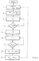
- Fig. 3 shows a diagram for schematically illustrating a procedure for sending in a radio network.
- data D for transmission is present in a first method step.
- the power amplifier 100 in the state “on” (PA E ) and also the driver 600 in the state “on” (BUF E ) is added.
- the power amplifier (PA) 100 is connected to the driver (BUF) 600 by continuously reducing the attenuation by the attenuator 700.
- the unmodulated carrier f LO (without data D) is applied during the continuous reduction.
- the carrier signal appears at the output 10 with a low power.
- n ⁇ 4 0 0 ⁇ 0
- the control circuit 500 can reset the counter 200 by means of the reset signal r.
- the count value n is compared with a register value reg in the register 400 by the comparator 300. If the count value n does not correspond to the register value reg, the count value n is increased again by one in the third step. If the count value n corresponds to the register value reg, a transfer (TX) of data D, which is transmitted by means of a transmission signal amplified by the power amplifier 100, takes place in the fifth step.
- TX transfer
- the count n is decremented by one in the sixth step (n-1).
- the signal connection between power amplifier (PA) 100 and driver (BUF) 600 is interrupted after continuously increasing the attenuation by the attenuator 700.
- the power amplifier 100 and the driver 600 are set in the "off" state (PA A , BUF A ).
- the signal input 106 is short-circuited by opening the transistor 160 to ground GND. If further data D are to be sent, the method can be continued in step 1.
- the invention is not limited to the illustrated embodiment variants of the figures.
- the functionality of the transmission cable according to Embodiment of Fig. 1 and the flowchart according to the embodiment of Fig. 3 is particularly advantageously used for a radio network of the industry standard IEEE 802.15.4.
Landscapes
- Engineering & Computer Science (AREA)
- Power Engineering (AREA)
- Computer Networks & Wireless Communication (AREA)
- Signal Processing (AREA)
- Transmitters (AREA)
- Amplifiers (AREA)
- Control Of Amplification And Gain Control (AREA)
Applications Claiming Priority (1)
| Application Number | Priority Date | Filing Date | Title |
|---|---|---|---|
| DE102008018914A DE102008018914A1 (de) | 2008-04-14 | 2008-04-14 | Sendeschaltung, Verfahren zum Senden und Verwendung |
Publications (3)
| Publication Number | Publication Date |
|---|---|
| EP2110954A2 true EP2110954A2 (fr) | 2009-10-21 |
| EP2110954A3 EP2110954A3 (fr) | 2011-05-18 |
| EP2110954B1 EP2110954B1 (fr) | 2012-08-01 |
Family
ID=40915477
Family Applications (1)
| Application Number | Title | Priority Date | Filing Date |
|---|---|---|---|
| EP09004816A Active EP2110954B1 (fr) | 2008-04-14 | 2009-04-01 | Circuit émetteur, procédé d'émission et d'utilisation |
Country Status (4)
| Country | Link |
|---|---|
| US (1) | US8041316B2 (fr) |
| EP (1) | EP2110954B1 (fr) |
| CN (1) | CN101562883B (fr) |
| DE (1) | DE102008018914A1 (fr) |
Cited By (2)
| Publication number | Priority date | Publication date | Assignee | Title |
|---|---|---|---|---|
| EP2495880A3 (fr) * | 2011-03-04 | 2013-05-22 | Fujitsu Semiconductor Limited | Procédé et système de réduction de l'incertitude temporelle de la transmission et la réception de données |
| US8787349B2 (en) | 2011-03-04 | 2014-07-22 | Intel IP Corporation | Method and system for reducing timing uncertainty of data transmission and reception |
Families Citing this family (2)
| Publication number | Priority date | Publication date | Assignee | Title |
|---|---|---|---|---|
| EP2996406B1 (fr) * | 2014-09-10 | 2020-07-15 | Nokia Solutions and Networks Oy | Procédé, appareil et programme informatique |
| CN106793050B (zh) * | 2017-01-04 | 2021-01-08 | 惠州Tcl移动通信有限公司 | 一种lte关断功率改善方法及系统 |
Citations (2)
| Publication number | Priority date | Publication date | Assignee | Title |
|---|---|---|---|---|
| EP0688109A2 (fr) | 1994-06-15 | 1995-12-20 | Nokia Mobile Phones Ltd. | Commande de puissance de sortie d'un émetteur impulsionnel et mise en forme d'enveloppe |
| US6983135B1 (en) | 2002-11-11 | 2006-01-03 | Marvell International, Ltd. | Mixer gain calibration method and apparatus |
Family Cites Families (14)
| Publication number | Priority date | Publication date | Assignee | Title |
|---|---|---|---|---|
| NL9000606A (nl) * | 1990-03-16 | 1991-10-16 | Ericsson Radio Systems Bv | Stelsel voor het met een herhaling uitzenden van alarmsignalen. |
| JP2800500B2 (ja) * | 1991-10-01 | 1998-09-21 | 松下電器産業株式会社 | バースト送信出力制御回路 |
| US5159283A (en) * | 1991-08-26 | 1992-10-27 | Motorola, Inc. | Power amplifier |
| JP2699824B2 (ja) * | 1993-09-28 | 1998-01-19 | 日本電気株式会社 | 可変レート伝送における伝送誤り訂正符号付加装置 |
| JP2924644B2 (ja) * | 1994-06-15 | 1999-07-26 | 三菱電機株式会社 | 送信電力制御回路、基地局、移動機及び移動体通信システム |
| US5548616A (en) * | 1994-09-09 | 1996-08-20 | Nokia Mobile Phones Ltd. | Spread spectrum radiotelephone having adaptive transmitter gain control |
| JPH08316756A (ja) * | 1995-05-22 | 1996-11-29 | Saitama Nippon Denki Kk | 送信出力制御方式 |
| DE19638772A1 (de) * | 1996-09-21 | 1998-03-26 | Philips Patentverwaltung | Telekommunikationsgerät, insbesondere Mobilfunkendgerät |
| DK1398874T3 (da) * | 2002-09-11 | 2005-09-05 | Siemens Ag | Fremgangsmåde og system til effektstyring i radiotransmittere |
| KR100604823B1 (ko) * | 2003-07-11 | 2006-07-26 | 삼성전자주식회사 | Gsm과 gprs 송신기의 전력 램핑 제어기 및 그 제어방법 |
| US8693950B2 (en) * | 2006-03-23 | 2014-04-08 | Broadcom Corporation | Method and system for transmit power control techniques to reduce mutual interference between coexistent wireless networks device |
| CN101043235B (zh) * | 2006-04-14 | 2010-10-27 | 华为技术有限公司 | 一种导频信号发射功率控制方法 |
| US7355477B2 (en) * | 2006-06-13 | 2008-04-08 | Agere Systems Inc. | Transmitter power control loop for high-speed wireless LANs |
| CN101035105B (zh) * | 2007-04-06 | 2010-11-03 | 西安电子科技大学 | 基于ifft/fft的预留子载波降低ofdm系统峰均功率比的方法和装置 |
-
2008
- 2008-04-14 DE DE102008018914A patent/DE102008018914A1/de not_active Withdrawn
-
2009
- 2009-04-01 EP EP09004816A patent/EP2110954B1/fr active Active
- 2009-04-14 US US12/423,565 patent/US8041316B2/en active Active
- 2009-04-14 CN CN2009101335637A patent/CN101562883B/zh not_active Expired - Fee Related
Patent Citations (2)
| Publication number | Priority date | Publication date | Assignee | Title |
|---|---|---|---|---|
| EP0688109A2 (fr) | 1994-06-15 | 1995-12-20 | Nokia Mobile Phones Ltd. | Commande de puissance de sortie d'un émetteur impulsionnel et mise en forme d'enveloppe |
| US6983135B1 (en) | 2002-11-11 | 2006-01-03 | Marvell International, Ltd. | Mixer gain calibration method and apparatus |
Cited By (2)
| Publication number | Priority date | Publication date | Assignee | Title |
|---|---|---|---|---|
| EP2495880A3 (fr) * | 2011-03-04 | 2013-05-22 | Fujitsu Semiconductor Limited | Procédé et système de réduction de l'incertitude temporelle de la transmission et la réception de données |
| US8787349B2 (en) | 2011-03-04 | 2014-07-22 | Intel IP Corporation | Method and system for reducing timing uncertainty of data transmission and reception |
Also Published As
| Publication number | Publication date |
|---|---|
| EP2110954A3 (fr) | 2011-05-18 |
| US20090257527A1 (en) | 2009-10-15 |
| EP2110954B1 (fr) | 2012-08-01 |
| CN101562883B (zh) | 2012-09-26 |
| DE102008018914A1 (de) | 2010-01-21 |
| US8041316B2 (en) | 2011-10-18 |
| CN101562883A (zh) | 2009-10-21 |
Similar Documents
| Publication | Publication Date | Title |
|---|---|---|
| DE102011055810B4 (de) | Nahfeldkommunikations-Leseeinrichtung | |
| DE60033995T2 (de) | Schaltung zur Antennenumschaltung und ein entsprechendes Kommunikationssystem | |
| DE69429223T2 (de) | Verfahren zur Parallelimpedanzanpassung für einen Sender und/oder Empfänger, sowie eine integrierte Schaltung und ein Übertragungssystem zur Durchführung des Verfahrens | |
| EP1522142B1 (fr) | Circuit amplificateur a amplification reglable et systeme emetteur comprenant un tel circuit amplificateur | |
| DE102018205304A1 (de) | Gate-Treiber | |
| DE112021004975T5 (de) | Verfahren, system und vorrichtung zum unterdrücken von schwingen eines controller area network bus | |
| WO2015067459A1 (fr) | Poste utilisateur pour système de bus et procédé de réduction des émissions liées au câblage dans un système de bus | |
| EP2110954B1 (fr) | Circuit émetteur, procédé d'émission et d'utilisation | |
| DE102020208635A1 (de) | Differenzsignal-übertragungsschaltung | |
| DE102013222782A1 (de) | Teilnehmerstation für ein Bussystem und Verfahren zur Reduzierung von leitungsgebundenen Emissionen in einem Bussystem | |
| DE102015204606A1 (de) | Sende- und Empfangsschaltung zum Übermitteln von differentiellen und single-ended Signalen über Übertragungsleitungen | |
| DE60110128T2 (de) | Sender mit aktivem differenzabschluss | |
| DE19630393C2 (de) | Elektrische Signalverarbeitungsschaltung | |
| DE19803796A1 (de) | Ausgangspuffer zum Ansteuern einer symmetrischen Übertragungsleitung | |
| DE10163466A1 (de) | Sendeanordnung für zeitkontinuierliche Datenübertragung | |
| DE102007007806A1 (de) | Dämpfungsglied | |
| DE102004039617B4 (de) | SBD-Sendeempfänger und SBD-Sendeempfängeranordnung | |
| DE10317936B4 (de) | Verstärkeranordnung und Sendeanordnung mit der Verstärkeranordnung | |
| DE10137150B4 (de) | Leitungstreiber zur Datenübertragung | |
| DE102008057619B4 (de) | Schaltungsanordnung zum Verstärken eines Digitalsignals und Transceiverschaltung für ein Bussystem | |
| DE10125023A1 (de) | Transmitter zur Übertragung digitaler Daten über eine Übertragungsleitung | |
| DE102016121865A1 (de) | Elektrische Schaltung zum Übertragen eines analogen Nutzsignals mit einer Kompensationsschaltung zum Kompensieren von Verzerrungen im Nutzsignal | |
| DE102017214144B4 (de) | Elektrische Schaltung für ein Common Mode Feedback System | |
| EP3884626A1 (fr) | Dispositif d'affaiblissement de réflexions pour un bus d'un système de bus et procédé d'affaiblissement de réflexions lors d'une transmission de données dans un système de bus | |
| DE60216660T2 (de) | Vorrichtung zur Leistungsregelung eines Senders |
Legal Events
| Date | Code | Title | Description |
|---|---|---|---|
| PUAI | Public reference made under article 153(3) epc to a published international application that has entered the european phase |
Free format text: ORIGINAL CODE: 0009012 |
|
| AK | Designated contracting states |
Kind code of ref document: A2 Designated state(s): AT BE BG CH CY CZ DE DK EE ES FI FR GB GR HR HU IE IS IT LI LT LU LV MC MK MT NL NO PL PT RO SE SI SK TR |
|
| PUAL | Search report despatched |
Free format text: ORIGINAL CODE: 0009013 |
|
| AK | Designated contracting states |
Kind code of ref document: A3 Designated state(s): AT BE BG CH CY CZ DE DK EE ES FI FR GB GR HR HU IE IS IT LI LT LU LV MC MK MT NL NO PL PT RO SE SI SK TR |
|
| AX | Request for extension of the european patent |
Extension state: AL BA RS |
|
| RIC1 | Information provided on ipc code assigned before grant |
Ipc: H04B 1/04 20060101AFI20090807BHEP Ipc: H03F 3/19 20060101ALI20110414BHEP |
|
| 17P | Request for examination filed |
Effective date: 20111117 |
|
| REG | Reference to a national code |
Ref country code: DE Ref legal event code: R079 Ref document number: 502009004204 Country of ref document: DE Free format text: PREVIOUS MAIN CLASS: H04B0001040000 Ipc: H03F0003240000 |
|
| GRAC | Information related to communication of intention to grant a patent modified |
Free format text: ORIGINAL CODE: EPIDOSCIGR1 |
|
| GRAP | Despatch of communication of intention to grant a patent |
Free format text: ORIGINAL CODE: EPIDOSNIGR1 |
|
| RIC1 | Information provided on ipc code assigned before grant |
Ipc: H03F 3/72 20060101ALI20120103BHEP Ipc: H03F 3/24 20060101AFI20120103BHEP |
|
| RIN1 | Information on inventor provided before grant (corrected) |
Inventor name: BEYER, SASCHA, DIPL.-ING. Inventor name: KLUGE, WOLFRAM, DR.-ING. Inventor name: FERCHLAND, TILO, DIPL.-ING. |
|
| GRAS | Grant fee paid |
Free format text: ORIGINAL CODE: EPIDOSNIGR3 |
|
| GRAA | (expected) grant |
Free format text: ORIGINAL CODE: 0009210 |
|
| AK | Designated contracting states |
Kind code of ref document: B1 Designated state(s): AT BE BG CH CY CZ DE DK EE ES FI FR GB GR HR HU IE IS IT LI LT LU LV MC MK MT NL NO PL PT RO SE SI SK TR |
|
| REG | Reference to a national code |
Ref country code: GB Ref legal event code: FG4D Free format text: NOT ENGLISH |
|
| REG | Reference to a national code |
Ref country code: CH Ref legal event code: EP Ref country code: AT Ref legal event code: REF Ref document number: 569111 Country of ref document: AT Kind code of ref document: T Effective date: 20120815 |
|
| REG | Reference to a national code |
Ref country code: IE Ref legal event code: FG4D Free format text: LANGUAGE OF EP DOCUMENT: GERMAN |
|
| REG | Reference to a national code |
Ref country code: DE Ref legal event code: R096 Ref document number: 502009004204 Country of ref document: DE Effective date: 20120927 |
|
| REG | Reference to a national code |
Ref country code: NL Ref legal event code: VDEP Effective date: 20120801 |
|
| REG | Reference to a national code |
Ref country code: LT Ref legal event code: MG4D Effective date: 20120801 |
|
| PG25 | Lapsed in a contracting state [announced via postgrant information from national office to epo] |
Ref country code: NO Free format text: LAPSE BECAUSE OF FAILURE TO SUBMIT A TRANSLATION OF THE DESCRIPTION OR TO PAY THE FEE WITHIN THE PRESCRIBED TIME-LIMIT Effective date: 20121101 Ref country code: IS Free format text: LAPSE BECAUSE OF FAILURE TO SUBMIT A TRANSLATION OF THE DESCRIPTION OR TO PAY THE FEE WITHIN THE PRESCRIBED TIME-LIMIT Effective date: 20121201 Ref country code: LT Free format text: LAPSE BECAUSE OF FAILURE TO SUBMIT A TRANSLATION OF THE DESCRIPTION OR TO PAY THE FEE WITHIN THE PRESCRIBED TIME-LIMIT Effective date: 20120801 Ref country code: HR Free format text: LAPSE BECAUSE OF FAILURE TO SUBMIT A TRANSLATION OF THE DESCRIPTION OR TO PAY THE FEE WITHIN THE PRESCRIBED TIME-LIMIT Effective date: 20120801 Ref country code: FI Free format text: LAPSE BECAUSE OF FAILURE TO SUBMIT A TRANSLATION OF THE DESCRIPTION OR TO PAY THE FEE WITHIN THE PRESCRIBED TIME-LIMIT Effective date: 20120801 Ref country code: CY Free format text: LAPSE BECAUSE OF FAILURE TO SUBMIT A TRANSLATION OF THE DESCRIPTION OR TO PAY THE FEE WITHIN THE PRESCRIBED TIME-LIMIT Effective date: 20120801 |
|
| PG25 | Lapsed in a contracting state [announced via postgrant information from national office to epo] |
Ref country code: SI Free format text: LAPSE BECAUSE OF FAILURE TO SUBMIT A TRANSLATION OF THE DESCRIPTION OR TO PAY THE FEE WITHIN THE PRESCRIBED TIME-LIMIT Effective date: 20120801 Ref country code: LV Free format text: LAPSE BECAUSE OF FAILURE TO SUBMIT A TRANSLATION OF THE DESCRIPTION OR TO PAY THE FEE WITHIN THE PRESCRIBED TIME-LIMIT Effective date: 20120801 Ref country code: PT Free format text: LAPSE BECAUSE OF FAILURE TO SUBMIT A TRANSLATION OF THE DESCRIPTION OR TO PAY THE FEE WITHIN THE PRESCRIBED TIME-LIMIT Effective date: 20121203 Ref country code: GR Free format text: LAPSE BECAUSE OF FAILURE TO SUBMIT A TRANSLATION OF THE DESCRIPTION OR TO PAY THE FEE WITHIN THE PRESCRIBED TIME-LIMIT Effective date: 20121102 Ref country code: SE Free format text: LAPSE BECAUSE OF FAILURE TO SUBMIT A TRANSLATION OF THE DESCRIPTION OR TO PAY THE FEE WITHIN THE PRESCRIBED TIME-LIMIT Effective date: 20120801 Ref country code: PL Free format text: LAPSE BECAUSE OF FAILURE TO SUBMIT A TRANSLATION OF THE DESCRIPTION OR TO PAY THE FEE WITHIN THE PRESCRIBED TIME-LIMIT Effective date: 20120801 |
|
| PG25 | Lapsed in a contracting state [announced via postgrant information from national office to epo] |
Ref country code: NL Free format text: LAPSE BECAUSE OF FAILURE TO SUBMIT A TRANSLATION OF THE DESCRIPTION OR TO PAY THE FEE WITHIN THE PRESCRIBED TIME-LIMIT Effective date: 20120801 |
|
| PG25 | Lapsed in a contracting state [announced via postgrant information from national office to epo] |
Ref country code: RO Free format text: LAPSE BECAUSE OF FAILURE TO SUBMIT A TRANSLATION OF THE DESCRIPTION OR TO PAY THE FEE WITHIN THE PRESCRIBED TIME-LIMIT Effective date: 20120801 Ref country code: CZ Free format text: LAPSE BECAUSE OF FAILURE TO SUBMIT A TRANSLATION OF THE DESCRIPTION OR TO PAY THE FEE WITHIN THE PRESCRIBED TIME-LIMIT Effective date: 20120801 Ref country code: ES Free format text: LAPSE BECAUSE OF FAILURE TO SUBMIT A TRANSLATION OF THE DESCRIPTION OR TO PAY THE FEE WITHIN THE PRESCRIBED TIME-LIMIT Effective date: 20121112 Ref country code: EE Free format text: LAPSE BECAUSE OF FAILURE TO SUBMIT A TRANSLATION OF THE DESCRIPTION OR TO PAY THE FEE WITHIN THE PRESCRIBED TIME-LIMIT Effective date: 20120801 Ref country code: DK Free format text: LAPSE BECAUSE OF FAILURE TO SUBMIT A TRANSLATION OF THE DESCRIPTION OR TO PAY THE FEE WITHIN THE PRESCRIBED TIME-LIMIT Effective date: 20120801 |
|
| PG25 | Lapsed in a contracting state [announced via postgrant information from national office to epo] |
Ref country code: IT Free format text: LAPSE BECAUSE OF FAILURE TO SUBMIT A TRANSLATION OF THE DESCRIPTION OR TO PAY THE FEE WITHIN THE PRESCRIBED TIME-LIMIT Effective date: 20120801 Ref country code: SK Free format text: LAPSE BECAUSE OF FAILURE TO SUBMIT A TRANSLATION OF THE DESCRIPTION OR TO PAY THE FEE WITHIN THE PRESCRIBED TIME-LIMIT Effective date: 20120801 |
|
| PLBE | No opposition filed within time limit |
Free format text: ORIGINAL CODE: 0009261 |
|
| STAA | Information on the status of an ep patent application or granted ep patent |
Free format text: STATUS: NO OPPOSITION FILED WITHIN TIME LIMIT |
|
| 26N | No opposition filed |
Effective date: 20130503 |
|
| REG | Reference to a national code |
Ref country code: DE Ref legal event code: R081 Ref document number: 502009004204 Country of ref document: DE Owner name: ATMEL CORP., US Free format text: FORMER OWNER: ATMEL AUTOMOTIVE GMBH, 74072 HEILBRONN, DE Effective date: 20130529 Ref country code: DE Ref legal event code: R081 Ref document number: 502009004204 Country of ref document: DE Owner name: ATMEL CORP., SAN JOSE, US Free format text: FORMER OWNER: ATMEL AUTOMOTIVE GMBH, 74072 HEILBRONN, DE Effective date: 20130529 Ref country code: DE Ref legal event code: R082 Ref document number: 502009004204 Country of ref document: DE Representative=s name: GRUENECKER PATENT- UND RECHTSANWAELTE PARTG MB, DE Effective date: 20130529 Ref country code: DE Ref legal event code: R082 Ref document number: 502009004204 Country of ref document: DE Representative=s name: GRUENECKER, KINKELDEY, STOCKMAIR & SCHWANHAEUS, DE Effective date: 20130529 |
|
| PG25 | Lapsed in a contracting state [announced via postgrant information from national office to epo] |
Ref country code: BG Free format text: LAPSE BECAUSE OF FAILURE TO SUBMIT A TRANSLATION OF THE DESCRIPTION OR TO PAY THE FEE WITHIN THE PRESCRIBED TIME-LIMIT Effective date: 20121101 |
|
| REG | Reference to a national code |
Ref country code: DE Ref legal event code: R097 Ref document number: 502009004204 Country of ref document: DE Effective date: 20130503 |
|
| BERE | Be: lapsed |
Owner name: ATMEL AUTOMOTIVE G.M.B.H. Effective date: 20130430 |
|
| PG25 | Lapsed in a contracting state [announced via postgrant information from national office to epo] |
Ref country code: MC Free format text: LAPSE BECAUSE OF FAILURE TO SUBMIT A TRANSLATION OF THE DESCRIPTION OR TO PAY THE FEE WITHIN THE PRESCRIBED TIME-LIMIT Effective date: 20120801 |
|
| REG | Reference to a national code |
Ref country code: CH Ref legal event code: PL |
|
| GBPC | Gb: european patent ceased through non-payment of renewal fee |
Effective date: 20130401 |
|
| REG | Reference to a national code |
Ref country code: IE Ref legal event code: MM4A |
|
| PG25 | Lapsed in a contracting state [announced via postgrant information from national office to epo] |
Ref country code: BE Free format text: LAPSE BECAUSE OF NON-PAYMENT OF DUE FEES Effective date: 20130430 Ref country code: CH Free format text: LAPSE BECAUSE OF NON-PAYMENT OF DUE FEES Effective date: 20130430 Ref country code: GB Free format text: LAPSE BECAUSE OF NON-PAYMENT OF DUE FEES Effective date: 20130401 Ref country code: LI Free format text: LAPSE BECAUSE OF NON-PAYMENT OF DUE FEES Effective date: 20130430 |
|
| REG | Reference to a national code |
Ref country code: FR Ref legal event code: ST Effective date: 20131231 |
|
| PG25 | Lapsed in a contracting state [announced via postgrant information from national office to epo] |
Ref country code: FR Free format text: LAPSE BECAUSE OF NON-PAYMENT OF DUE FEES Effective date: 20130430 |
|
| PG25 | Lapsed in a contracting state [announced via postgrant information from national office to epo] |
Ref country code: IE Free format text: LAPSE BECAUSE OF NON-PAYMENT OF DUE FEES Effective date: 20130401 |
|
| PG25 | Lapsed in a contracting state [announced via postgrant information from national office to epo] |
Ref country code: MT Free format text: LAPSE BECAUSE OF FAILURE TO SUBMIT A TRANSLATION OF THE DESCRIPTION OR TO PAY THE FEE WITHIN THE PRESCRIBED TIME-LIMIT Effective date: 20120801 |
|
| REG | Reference to a national code |
Ref country code: AT Ref legal event code: MM01 Ref document number: 569111 Country of ref document: AT Kind code of ref document: T Effective date: 20140401 |
|
| PG25 | Lapsed in a contracting state [announced via postgrant information from national office to epo] |
Ref country code: TR Free format text: LAPSE BECAUSE OF FAILURE TO SUBMIT A TRANSLATION OF THE DESCRIPTION OR TO PAY THE FEE WITHIN THE PRESCRIBED TIME-LIMIT Effective date: 20120801 |
|
| PG25 | Lapsed in a contracting state [announced via postgrant information from national office to epo] |
Ref country code: HU Free format text: LAPSE BECAUSE OF FAILURE TO SUBMIT A TRANSLATION OF THE DESCRIPTION OR TO PAY THE FEE WITHIN THE PRESCRIBED TIME-LIMIT; INVALID AB INITIO Effective date: 20090401 Ref country code: MK Free format text: LAPSE BECAUSE OF FAILURE TO SUBMIT A TRANSLATION OF THE DESCRIPTION OR TO PAY THE FEE WITHIN THE PRESCRIBED TIME-LIMIT Effective date: 20120801 Ref country code: LU Free format text: LAPSE BECAUSE OF NON-PAYMENT OF DUE FEES Effective date: 20130401 |
|
| PG25 | Lapsed in a contracting state [announced via postgrant information from national office to epo] |
Ref country code: AT Free format text: LAPSE BECAUSE OF NON-PAYMENT OF DUE FEES Effective date: 20140401 |
|
| P01 | Opt-out of the competence of the unified patent court (upc) registered |
Effective date: 20230528 |
|
| PGFP | Annual fee paid to national office [announced via postgrant information from national office to epo] |
Ref country code: DE Payment date: 20250319 Year of fee payment: 17 |