EP2113823A2 - Appareil de traitement en paquets - Google Patents
Appareil de traitement en paquets Download PDFInfo
- Publication number
- EP2113823A2 EP2113823A2 EP20090155891 EP09155891A EP2113823A2 EP 2113823 A2 EP2113823 A2 EP 2113823A2 EP 20090155891 EP20090155891 EP 20090155891 EP 09155891 A EP09155891 A EP 09155891A EP 2113823 A2 EP2113823 A2 EP 2113823A2
- Authority
- EP
- European Patent Office
- Prior art keywords
- packet
- unit
- clock
- buffer
- packet data
- Prior art date
- Legal status (The legal status is an assumption and is not a legal conclusion. Google has not performed a legal analysis and makes no representation as to the accuracy of the status listed.)
- Granted
Links
Images


Classifications
-
- G—PHYSICS
- G06—COMPUTING OR CALCULATING; COUNTING
- G06F—ELECTRIC DIGITAL DATA PROCESSING
- G06F1/00—Details not covered by groups G06F3/00 - G06F13/00 and G06F21/00
- G06F1/26—Power supply means, e.g. regulation thereof
- G06F1/32—Means for saving power
- G06F1/3203—Power management, i.e. event-based initiation of a power-saving mode
-
- G—PHYSICS
- G06—COMPUTING OR CALCULATING; COUNTING
- G06F—ELECTRIC DIGITAL DATA PROCESSING
- G06F1/00—Details not covered by groups G06F3/00 - G06F13/00 and G06F21/00
- G06F1/26—Power supply means, e.g. regulation thereof
- G06F1/32—Means for saving power
- G06F1/3203—Power management, i.e. event-based initiation of a power-saving mode
- G06F1/3234—Power saving characterised by the action undertaken
- G06F1/3237—Power saving characterised by the action undertaken by disabling clock generation or distribution
-
- Y—GENERAL TAGGING OF NEW TECHNOLOGICAL DEVELOPMENTS; GENERAL TAGGING OF CROSS-SECTIONAL TECHNOLOGIES SPANNING OVER SEVERAL SECTIONS OF THE IPC; TECHNICAL SUBJECTS COVERED BY FORMER USPC CROSS-REFERENCE ART COLLECTIONS [XRACs] AND DIGESTS
- Y02—TECHNOLOGIES OR APPLICATIONS FOR MITIGATION OR ADAPTATION AGAINST CLIMATE CHANGE
- Y02D—CLIMATE CHANGE MITIGATION TECHNOLOGIES IN INFORMATION AND COMMUNICATION TECHNOLOGIES [ICT], I.E. INFORMATION AND COMMUNICATION TECHNOLOGIES AIMING AT THE REDUCTION OF THEIR OWN ENERGY USE
- Y02D10/00—Energy efficient computing, e.g. low power processors, power management or thermal management
-
- Y—GENERAL TAGGING OF NEW TECHNOLOGICAL DEVELOPMENTS; GENERAL TAGGING OF CROSS-SECTIONAL TECHNOLOGIES SPANNING OVER SEVERAL SECTIONS OF THE IPC; TECHNICAL SUBJECTS COVERED BY FORMER USPC CROSS-REFERENCE ART COLLECTIONS [XRACs] AND DIGESTS
- Y02—TECHNOLOGIES OR APPLICATIONS FOR MITIGATION OR ADAPTATION AGAINST CLIMATE CHANGE
- Y02D—CLIMATE CHANGE MITIGATION TECHNOLOGIES IN INFORMATION AND COMMUNICATION TECHNOLOGIES [ICT], I.E. INFORMATION AND COMMUNICATION TECHNOLOGIES AIMING AT THE REDUCTION OF THEIR OWN ENERGY USE
- Y02D30/00—Reducing energy consumption in communication networks
- Y02D30/50—Reducing energy consumption in communication networks in wire-line communication networks, e.g. low power modes or reduced link rate
Definitions
- the present invention relates to a packet processing apparatus, in particular a packet processing apparatus to process packet data at timing based on a clock signal.
- the electronic devices such as computers and servers
- they usually have relatively long time periods during which no operations are carried out (the so-called "standby state"). It is possible to reduce the average power consumption of such electronic devices by reducing power consumption while the electronic devices are in the standby state, and thereby to make a significant contribution to the reduction of carbon dioxide emissions calculated from the average power consumption.
- the information communication devices although they has been converted from analog communication devices to digital communication devices, they are still required to be constantly maintained in the state capable of carrying out data communications. Therefore, in the case of information communication devices, there is a prerequisite that, unlike the electronic devices such as computers and servers, the standby state is not feasible. That is, in the case of information communication devices, it is necessary to reduce electrical power in the normal operation state to reduce the average power consumption.
- a packet is firstly input from a packet input terminal 111 to a packet buffer F-unit 112 in synchronization with a clock input from an input clock input terminal 131.
- the packet is accumulated at the buffer F-unit 112.
- the packet accumulated at the packet buffer F-unit 112 is output to a packet processing A-unit 113 where a first packet process A is to be carried out.
- the process A is carried out on the packet at the packet processing A-unit.
- the packet for which the process A is completed at the packet processing A-unit 113 is delivered via a clock transfer D-unit 114 to a packet processing B-unit 115 where a second packet process B is to be carried out.
- the process B is carried out on the packet in the packet processing B-unit 115.
- the packet for which the process B is completed at the packet processing B-unit 115 is delivered via a clock transfer E-unit 116 to a packet processing C-unit 117 where a third packet process C is to be carried out.
- the process C is carried out on the packet in the packet processing C-unit 117.
- the packet for which the process C is completed at the packet processing C-unit 117 is delivered to a packet buffer G-unit 118, and output from the packet output terminal 119 in synchronization with a clock input from an output clock input terminal 132. Furthermore, a clock distribution unit 140 generates clocks 1, 2, and 3 having appropriate frequencies required in the respective constitutional blocks from a reference clock input from a reference clock input terminal 134. The clock distribution unit 140 supplies the generated clocks to the respective constitutional blocks.
- the clocks are constantly supplied from the clock distribution unit 140 even when no packet exists in the packet processing A-unit, the packet processing B-unit, and the packet processing C-unit and thereby no packet processing operations are required. Since the clocks are constantly supplied even when packet processing is not required in any of the packet processing units, each unit consumes electrical power in a constant manner. That is, it causes power consumption called "standby power consumption" in the above-described configuration. As a result, the average operating power consumption is never reduced by a large amount even when the traffic is low, and therefore it is impossible to achieve power savings.
- Patent document 1 Japanese Unexamined Patent Application No. 2006-345278
- Patent document 2 Japanese Unexamined Patent Application No. 2004-274099
- Patent document 2 in a case where a constantly-operating macro and an intermittently-operating macro are arranged in series, when it is detected that no packet is output from the constantly-operating macro at the preceding stage for a certain time period, the supply of the clock to the intermittently-operating macro at the subsequent stage is suspended.
- An exemplary object of the present invention is to reduce the power consumption without the loss of the throughput in a packet communication device in which the incoming traffic capacity varies.
- An exemplary aspect of the present invention is a packet processing apparatus including: a packet buffer unit that temporarily holds packet data; a packet processing unit that processes packet data output from the packet buffer unit; a clock supply unit that supplies a clock signal to the packet processing unit; and a control unit that detects a buffer vacant time indicating a time during which no packet data exists in the packet buffer unit based on an accumulation amount of the packet data in the packet buffer unit, and controls an operational state of the clock supply unit in accordance with the buffer vacant time.
- another exemplary aspect of the present invention is a computer program including: measuring a buffer vacant time indicating a time during which no packet data exists within a packet buffer unit based on an accumulation amount of the packet data in the packet buffer unit, the packet buffer unit being configured to temporarily store the packet data; and controlling an operational state of a clock supply unit in accordance with the buffer vacant time, the clock supply unit being configured to supply a clock signal defining the processing of a packet processing unit to the packet processing unit, the packet processing unit being configured to process the packet data output from the packet buffer unit.
- another exemplary aspect of the present invention is a clock control method including: measuring a buffer vacant time indicating a time during which no packet data exists within a packet buffer unit based on an accumulation amount of the packet data in the packet buffer unit, the packet buffer unit being configured to temporarily store the packet data; and controlling an operational state of a clock supply unit in accordance with the buffer vacant time, the clock supply unit being configured to supply a clock signal to the packet processing unit, the packet processing unit being configured to process the packet data output from the packet buffer unit.
- the present invention has an excellent exemplary advantage that the supply operation of a clock signal is changed while suppressing decrease in the throughput of packet data so that the input packet data is continuously processed, and therefore the power consumption of the apparatus can be reduced.
- a exemplary aspect of a packet processing apparatus in accordance with an exemplary embodiment of the present invention is that a time during which the accumulation amount of incoming packet data is "0" is measured, and the supply operation of a clock signal for causing a packet processing unit to operate is changed based on the measured time.
- a packet processing apparatus in accordance with an example embodiment includes: a packet buffer unit that accepts and temporarily holds an input of packet data divided into predefined processing units; a packet processing unit that processes packet data output from the packet buffer unit; and a clock control unit that supplies a clock signal to the packet processing unit for causing the packet processing unit to operate.
- the packet processing apparatus further includes a buffer vacant time detection unit that detects the accumulation amount of packet data in the packet buffer unit and indicates a time during which no packet data exists in the packet buffer unit.
- the clock control unit controls the supply operation of the clock signal to the packet processing unit based on the buffer vacant time detected in the buffer vacant time detection unit.
- the above-mentioned clock control unit controls the supply operation of the clock signal in such a manner that the supply operation of the clock signal to the packet processing unit is suspended, or that the frequency of the clock signal is set at a lower value and the clock signal is supplied to the packet processing unit.
- packet data to be processed is firstly input to the packet buffer and accumulated in the packet buffer unit. Then, the packet data is output from the packet buffer unit to the packet processing unit in order. Then, the packet data is processed in the packet processing unit at operation timing based on the clock signal supplied to the packet processing unit.
- the accumulation amount of the packet data in the above-mentioned packet buffer unit is detected, and a time during which no packet data exists in the packet buffer unit is measured.
- the supply operation of the clock signal to the above-mentioned packet processing unit is changed in accordance with the measured time during which no packet data exists. For example, the supply of the clock signal may be suspended, or the clock signal may continue to be supplied to the packet processing unit while the frequency of the clock signal is set at a lower value.
- the supply operation of the clock signal to the packet processing unit is changed in accordance with the input state of incoming packet data so that no influence is exerted on the data processing. Therefore, the supply of the clock signal is suspended while suppressing decrease in the throughput of packet data so that the input packet data is continuously processed, and therefore the power consumption of the apparatus can be reduced.
- the above-mentioned clock control unit compares a buffer vacant time measured in the buffer vacant time detection unit with a comparison reference time that is determined in advance based on the number of packet processing units that process packet data, and controls the supply operation of the clock signal to the packet processing unit based on the comparison result.
- the above-mentioned comparison reference time is a time in which packet data is processed in all of the packet processing units, and the above-mentioned clock control unit suspends the supply of the clock signal to the packet processing unit if the buffer vacant time is larger than the comparison reference time.
- the above-mentioned buffer vacant time detection unit is configured to detect a situation where packet data is input to the packet buffer unit within which no packet exists until that moment.
- the above-mentioned clock control unit is configured, when the supply operation of the clock signal to the packet processing unit is being suspended, to start the supply operation of the clock signal to the packet processing unit when the above-mentioned buffer vacant time detection unit detects an input of packet data.
- the supply of the clock signal to the packet processing unit is suspended.
- the supply of the clock signal can be suspended without causing any problem. Therefore, the power consumption can be reduced.
- the supply of the clock signal is promptly resumed and the packet processing unit becomes ready to operate. Therefore, the input packet data can be processed, and decrease in the throughput can be suppressed.
- packet processing apparatuses are not limited to those examples.
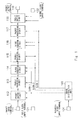
- FIG. 2 is a functional block diagram illustrating one example of a packet communication device
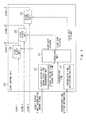
- Fig. 3 is a functional block diagram illustrating a configuration of a clock control unit
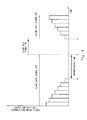
- Fig. 4 is an explanatory diagram illustrating the relation between packet accumulation amounts and a clock supply operation
- Fig. 5 is a flowchart illustrating an operation of the clock control unit.
- Fig. 2 shows a configuration of a router or a switch, which is one example of a packet communication device, and in particular, a configuration of the packet processing function of a packet communication device that performs packet processing.
- a packet communication device such as a router and a switch includes a packet input terminal 11, a packet buffer F-unit 21, a packet processing A-unit 13, a clock transfer D-unit 14, a packet processing B-unit 15, a clock transfer E-unit 16, a packet processing C-unit 17, a packet buffer G-unit 16, a packet output terminal 19, a clock control unit 20, a clock distribution unit 40, an input clock input terminal 31, an output clock input terminal 32, a transmission time setting information input terminal 33, and a reference clock input terminal 34.
- the packet communication device further includes a packet buffer F-unit 12 (packet buffer unit).
- the packet buffer F-unit 12 accepts an input of packet data divided into predefined data processing units (hereinafter called "packet") from a packet input terminal 11 in synchronization with a clock input from an input clock input terminal 31, and temporarily accumulates it.
- the packet buffer F-unit 12 sends an accumulation amount signal to the clock control unit 20 at regular time intervals or whenever an input of a packet is accepted.
- the accumulation amount signal indicates a packet accumulation amount within the packet buffer F-unit 21.
- the maximum accumulation amount of the packet buffer F-unit 12 is equal to or larger than a packet amount corresponding to a time required to transmit a packet through a path formed by the packet processing A-unit 13 to the packet processing C-unit 17.
- the maximum packet accumulation amount is the maximum number of packets that can be output by the packet buffer F-unit 12 while a time in which one packet output from the packet, buffer F-unit 12 is processed in a series of the processing-units (including packet processing units 13, 15, and 17, and clock transfer units 14 and 16) elapses.
- the series of processing units are formed from a plurality of processing-units that are located at subsequent stages to the packet buffer F-unit 12 and are to process that packet.
- the maximum accumulation amount of the packet buffer F-unit is not limited to the above-mentioned amount.
- the packet, buffer F-unit 12 outputs the accumulated packet to the packet processing A-unit 13 based on a clock supplied from the clock distribution unit 40.
- the packet processing A-unit 13 performs a first packet process A on the input packet in synchronization with a clock A supplied from the clock control unit 20.
- the packet processing A-unit 13 outputs the packet on which the process A is completed to the clock transfer D-unit 14. In this manner, the packet on which the process A is completed is output to the packet processing B-unit 15 via the clock transfer D-unit 14.
- the packet processing B-unit 15 performs a second packet process B on the input packet in synchronization with a clock B supplied from the clock control unit 20.
- the packet processing B-unit 15 outputs the packet on which the process B is completed to the clock transfer E-unit 16.
- the packet on which the process B is completed is output to the packet processing C-unit 17 via the clock transfer E-unit 16.
- the packet processing C-unit 17 performs a third packet process C on the input packet in synchronization with a clock C supplied from the clock control unit 20. Then, the packet on which the process C is completed in the packet processing C-unit 17 is output to a packet buffer G-unit 18, and the packet buffer G-unit 18 outputs the packet from the packet output terminal 19 in synchronization with a clock input from the output clock input terminal 32.
- the clock distribution unit 40 generates clocks 1, 2, and 3 having appropriate frequencies for the respective blocks (such as the clock control unit 20) from a reference clock input from the reference clock input terminal 34.
- the clock distribution unit 40 supplies the generated clocks to the respective blocks. Specifically, as illustrated in Fig. 2 , the clock distribution unit 40 supplies the clock 1 to the packet buffer F-unit 12, the clock transfer D-unit 14, and the clock control unit 20.
- the clock distribution unit 40 supplies the clock 2 to the clock transfer D-unit 14, the clock transfer E-unit 16, and the clock control unit 20.
- the clock distribution unit 40 supplies the clock 3 to the clock transfer E-unit 16, the packet buffer G-unit 18, and the clock control unit 20.
- the clock frequencies are defined as three clocks, i.e., the clock 1, 2, and 3 for simplifying the explanation, a plurality of clock frequencies may be supplied to each constitutional block.
- the clock distribution unit 40 supplies three clocks, i.e., the clock 1, 2, and 3 to the clock control unit 20.
- the clock control unit 20 supplies a clock A, B, and C to the packet processing A-unit 13, the packet, processing B-unit 15, and the packet processing C-unit 17, respectively, based on the respective input clocks.
- the clock control unit 20 includes a packet buffer F-unit vacant state time measurement unit 21, a transmission time registration register 22, and a comparison unit 23.
- the function of the clock, control unit 20 can be realized by incorporating a certain computer program into an arithmetic unit constituting the clock control unit. That is, the blocks 21 to 23 are constructed by incorporating a certain computer program(s).
- the clock control unit 20 further includes a clock A-gate-unit 24, a clock B-gate-unit 25, and a clock C-gate-unit 26.
- the gate-unit 24 outputs a clock A based on an input of the clock 1.
- the other gate units 25 and 26 operate in a similar manner.
- the operational state of the gate-unit 24 is determined based on a gate A-signal output from the comparison unit 23.
- the gate A-signal indicates "gate ON”
- the gate-unit 24 enters a state where it does not output the clock A in accordance with the clock 1.
- the gate A-signal indicates "gate OFF”
- the gate-unit 24 enters a state where it outputs the clock A in accordance with the clock 1.
- the other gate units 25 and 26 operate in a similar manner.
- the gate-unit 24 forms a clock supply unit that supplies the clock A to the packet processing A-unit 13.
- the other gate units 25 and 26 operate in a similar manner. It is also possible to consider all of the gate units 24 to 26 as the clock supply unit. Note that the gate units 24 to 26 may also be recognized as switches for supplying or not supplying the corresponding clocks.
- the packet buffer F-unit vacant state time measurement unit 21 (hereinafter sometimes called as “buffer vacant time measurement unit” or “buffer vacant time detection unit”) accepts a packet buffer F-unit accumulation amount signal (hereinafter called “accumulation amount signal”) sent from the packet buffer F-unit 12.
- the buffer vacant time measurement unit 21 measures a time during which no packet is accumulated (there is no accumulated packet) in the packet buffer F-unit based on the accepted accumulation amount signal. In other words, the buffer vacant time measurement unit 21 simply detects the certain period of time in which no packet is accumulated in the packet buffer F-unit.
- the buffer vacant time measurement unit 21 performs this measurement at regular intervals or whenever the above-mentioned accumulation amount signal is received.
- the buffer vacant time measurement unit 21 delivers the measured packet buffer F-unit vacant state time to the comparison unit 23.
- the buffer vacant time measurement unit 21 measures a time (horizontal axis) during which the packet buffer F-unit accumulation amount (vertical axis) remains at “0", as shown between the time "a" and the times "b" and "c".
- the buffer vacant time measurement unit 21 notifies the comparison unit 23 that the packet buffer F-unit vacant state time is "0". This is because since the packet buffer accumulation amount is no longer "0", packet buffer F-unit vacant state time cannot be measured.
- the transmission time registration register 22 receives transmission time setting information (comparison reference time) input from the transmission time setting information input terminal 33, and stores as a transmission time.
- the transmission time registration register 22 outputs the stored transmission time information to the comparison unit 23.
- the above-mentioned transmission time setting information corresponds to a time required to complete the process of one packet accumulated in and output from the above-mentioned packet buffer F-unit 12 by transmitting it through the packet processing A-unit 13 to the packet processing C-unit 17.
- the transmission time setting information indicates a time in which one packet output from the packet buffer F-unit 12 is processed in all the processing-units that are located at subsequent stages to the packet buffer F-unit 12 and are to process that packet (including packet processing units 13, 15, and 17, and clock transfer units 14 and 16).
- the above-mentioned comparison unit 23 compares a packet buffer F-unit vacant state time output from the buffer vacant time measurement unit 21 with a transmission time output from the transmission time registration register 22. Note that this comparison may be carried out whenever a measurement result is notified from The buffer vacant time measurement unit 21, or at regular time intervals.
- the comparison unit 23 indicates that the packet buffer F-unit vacant state time has become larger than the transmission time as shown in the period at or later than the time "b" in Fig. 4 , the comparison unit 23 operates in the following manner.
- the comparison unit 23 outputs a clock gate A-signal, a clock gate B-signal, and a clock gate C-signal all of which are in "gate ON” states to the clock A-gate-unit 24, the clock B-gate-unit 25, and the clock C-gate-unit 26 respectively.
- the "gate ON" signals are control signals used to control the respective gate units 24, 25, and 26 such that they suspend the output of clocks. Therefore, the gate units 24, 25, and 26 that received the "gate ON” signals suspend the clock outputs to their respective packet processing units 13, 15, and 17.
- the comparison unit 23 outputs the clock gate A-signal, the clock gate B-signal, and the clock gate C-signal all of which are in "gate OFF" states except when the above-mentioned comparison result indicates that the packet buffer F-unit vacant state time is larger than the transmission time.
- the "gate OFF" signals are control signals used to control the respective gate units 24, 25, and 26 such that they output the clocks.
- the comparison unit 23 (clock control unit 20) constantly supplies the clock signals to the packet processing units 13, 15, and 17 in the period at or earlier than the time "b" (even when the accumulation amount is "0", its duration, i.e., the packet buffer F-unit vacant state time (buffer vacant time) has not exceeded the transmission time), or in the period at or later than the time "c" (when the packet buffer F-unit accumulation amount is not "0") in Fig. 4 .
- the comparison unit 23 suspends the supply of the clock signals during that period. In this way, the clock supply operation by the clock control unit 20 is changed.
- the comparison unit 23 starts supplying the clock signals to the packet processing units 13, 15, and 17. In this manner, the clock supply operation by the clock control unit 20 is changed from the state where the clock signals are not supplied to the state where the clock signals are supplied.
- the clock supply to the respective packet processing units 13, 15, and 17 is suspended has been illustrated.
- the timing at which the supply to the packet processing units 13, 15, and 17 is suspended is not limited to the timing described above.
- the transmission time with which the packet buffer F-unit vacant state time is compared is not necessarily limited to the value described above.
- the clock supply operation may be changed in such a manner that the clock supply is suspended in accordance with other decision criteria based on the above-mentioned packet buffer F-unit vacant state time.
- the clock control unit 20 accepts an accumulation amount signal sent from the packet buffer F-unit 12 in the buffer vacant time measurement unit 21 (Step S1). Then, when an incoming packet(s) is accumulated within the packet buffer F-unit 12 ("No" at Step S2, at or before time “a” in Fig. 4 ), the buffer vacant time measurement unit 21 clears the packet buffer vacant state time (sets to "0") (Step S6), and remains in the state where the clocks are being supplied to the packet processing units 13, 15, and 17 (Step S7).
- the comparison unit 23 continues to output "gate OFF" signals to the respective gate units 24, 25, and 26, these respective clock gate units 24, 25, and 26 continue to supply the clock signals to the respective packet processing units 13, 15, and 17, and the packet(s) accumulated in the packet buffer F-unit 12 is processed in the packet processing units and the like.
- Step S3 Buffer vacant time measuring step.
- the measured packet buffer vacant state time is compared with a transmission time registered in the transmission time registration register in the comparison unit 23 (Step S4), At this point, if the packet buffer vacant state time has not exceeded the transmission time ("No” at Step S4, before time “b” in Fig. 4 ), the comparison unit 23 continues to output "gate OFF" signals to the respective clock gate units 24, 25, and 26. In this way, the clock signals continue to be supplied from these clock gate units 24, 25, and 26 to the respective packet processing units 13, 15, and 17 (Step S7), and the packet(s) accumulated in the packet buffer F-unit 12 is processed in the packet processing units and the like.
- the buffer vacant time measurement unit 21 detects that the accumulation amount signal from the packet buffer F-unit 12 is changed from "0" to a value other than "0", i.e., a packet (s) is accumulated again (Step S1, "No” at Step S2, Buffer vacant time measuring step, at or after time “c” in Fig. 4 ), the buffer vacant state time is cleared (set to "0") (Step S6) and the clock supply to the packet processing units 13, 15, and 17 is resumed (Step S7, Clock supply operation changing step). That is, since the buffer vacant state time becomes "0", the comparison unit 23 outputs "gate OFF" signals to the respective gate units 24, 25, and 26. In this way, these gate units 24, 25, and 26 enter a state where they continuously supply the clock signals to the respective packet processing units 13, 15, and 17. Then, the packet(s) accumulated in the packet buffer F-unit 12 is processed in the packet processing units and the like.
- a time during which no packet data exists within the packet buffer F-unit 12 is measured, and the supply operation of the clock signals to the packet processing units 13, 15, and 17 is changed in accordance with the measured time during which no packet data exists. For example, when a time during which no packet data is accumulated exceeds the time required for a series of processes for one packet, i.e., the transmission time, the supply of the clock signals is suspended. In this way, the supply of a clock signal to a packet, processing unit is suspended only when no packet to be processed is accumulated. Therefore, the power consumption can be reduced without causing any influence to the throughput. Meanwhile, when packet data is accumulated in the packet buffer F-unit 12, the supply of the clock signal is resumed. Therefore, the process on that packet data can be promptly resumed, and decrease in the throughput can be suppressed.
- the clock control unit 20 may set the frequency of the supplied clock at lower value and supply the clock signal having the lowered frequency to the packet, processing unit and the like, instead of completely stopping the supply of the clock signal. Even with such a configuration, the power consumption involved in the clock supply operation can be reduced when there is no packet to be processed in the packet buffer F-unit 12.
- N packet processing units and (N-1) clock transfer units may be arranged in subsequent stages to the packet buffer F-unit 12. Furthermore, any other number of packet processing units may be arranged.
- the packet processing apparatus in accordance with an exemplary embodiment of the present invention can be applied to packet processing apparatuses in which an input of packet data is put in a standby state (such as routers and switches).
Landscapes
- Engineering & Computer Science (AREA)
- Theoretical Computer Science (AREA)
- Physics & Mathematics (AREA)
- General Engineering & Computer Science (AREA)
- General Physics & Mathematics (AREA)
- Data Exchanges In Wide-Area Networks (AREA)
- Communication Control (AREA)
- Power Sources (AREA)
Applications Claiming Priority (1)
| Application Number | Priority Date | Filing Date | Title |
|---|---|---|---|
| JP2008111943A JP4962396B2 (ja) | 2008-04-23 | 2008-04-23 | パケット処理装置 |
Publications (3)
| Publication Number | Publication Date |
|---|---|
| EP2113823A2 true EP2113823A2 (fr) | 2009-11-04 |
| EP2113823A3 EP2113823A3 (fr) | 2016-06-15 |
| EP2113823B1 EP2113823B1 (fr) | 2021-04-21 |
Family
ID=41091810
Family Applications (1)
| Application Number | Title | Priority Date | Filing Date |
|---|---|---|---|
| EP09155891.6A Active EP2113823B1 (fr) | 2008-04-23 | 2009-03-23 | Appareil de traitement en paquets |
Country Status (4)
| Country | Link |
|---|---|
| US (1) | US8279787B2 (fr) |
| EP (1) | EP2113823B1 (fr) |
| JP (1) | JP4962396B2 (fr) |
| CN (2) | CN104898819B (fr) |
Families Citing this family (8)
| Publication number | Priority date | Publication date | Assignee | Title |
|---|---|---|---|---|
| JP5007703B2 (ja) * | 2008-05-19 | 2012-08-22 | 日本電気株式会社 | パケット処理装置、パケット制御方法及びパケット制御プログラム |
| JP5482466B2 (ja) * | 2010-06-03 | 2014-05-07 | 富士通株式会社 | データ転送装置及びデータ転送装置の動作周波数制御方法 |
| US9880603B1 (en) | 2013-03-13 | 2018-01-30 | Juniper Networks, Inc. | Methods and apparatus for clock gating processing modules based on hierarchy and workload |
| US9477257B1 (en) | 2013-03-13 | 2016-10-25 | Juniper Networks, Inc. | Methods and apparatus for limiting a number of current changes while clock gating to manage power consumption of processor modules |
| JP5948361B2 (ja) * | 2014-03-28 | 2016-07-06 | 株式会社Pfu | 情報処理装置、および、出力調整方法 |
| US9698781B1 (en) * | 2016-05-26 | 2017-07-04 | Intel Corporation | Dynamic clock gating frequency scaling |
| KR102618563B1 (ko) * | 2016-07-01 | 2023-12-27 | 삼성전자주식회사 | 집적 회로 장치와 이를 포함하는 전자 장치 |
| US11175836B2 (en) * | 2019-03-01 | 2021-11-16 | Qualcomm Incorporated | Enhanced data clock operations in memory |
Family Cites Families (22)
| Publication number | Priority date | Publication date | Assignee | Title |
|---|---|---|---|---|
| US5461266A (en) * | 1990-11-27 | 1995-10-24 | Hitachi, Ltd. | Power consumption control system |
| JPH10268963A (ja) * | 1997-03-28 | 1998-10-09 | Mitsubishi Electric Corp | 情報処理装置 |
| JPH10275140A (ja) * | 1997-03-31 | 1998-10-13 | Nec Ic Microcomput Syst Ltd | マイクロコンピュータ |
| JP3573957B2 (ja) * | 1998-05-20 | 2004-10-06 | インターナショナル・ビジネス・マシーンズ・コーポレーション | コンピュータ内のプロセッサの動作速度制御方法及びコンピュータ |
| US6647502B1 (en) * | 1999-07-13 | 2003-11-11 | Sony Corporation | Method and apparatus for providing power based on the amount of data stored in buffers |
| JP4256546B2 (ja) * | 1999-08-24 | 2009-04-22 | パナソニック株式会社 | ストリーム多重分離装置 |
| GB2355899A (en) * | 1999-10-29 | 2001-05-02 | Oak Technology Inc | Multistage digital processor with dedicated stage clock controllers |
| KR100487543B1 (ko) | 2000-09-01 | 2005-05-03 | 엘지전자 주식회사 | 시피유 스케쥴링 방법 |
| JP3877518B2 (ja) * | 2000-12-13 | 2007-02-07 | 松下電器産業株式会社 | プロセッサの電力制御装置 |
| JP3819242B2 (ja) * | 2001-02-09 | 2006-09-06 | 株式会社日立製作所 | 断続信号を扱う無線通信装置 |
| US6990598B2 (en) * | 2001-03-21 | 2006-01-24 | Gallitzin Allegheny Llc | Low power reconfigurable systems and methods |
| US6785831B2 (en) * | 2001-12-06 | 2004-08-31 | Matsushita Electric Industrial Co., Ltd. | Power consumption management apparatus |
| JP2003304224A (ja) * | 2002-04-08 | 2003-10-24 | Toshiba Corp | データ伝送装置 |
| JP2004078581A (ja) * | 2002-08-19 | 2004-03-11 | Nec Corp | 通信データ処理回路 |
| JP4093034B2 (ja) * | 2002-12-02 | 2008-05-28 | オンキヨー株式会社 | コンテンツ送受信システム及びコンテンツ送信装置 |
| JP2004274099A (ja) * | 2003-03-05 | 2004-09-30 | Nec Corp | パケット処理回路 |
| JP2005286749A (ja) * | 2004-03-30 | 2005-10-13 | Matsushita Electric Ind Co Ltd | 映像復号化装置およびそれを用いた映像伝送システム |
| US7206950B2 (en) * | 2004-06-16 | 2007-04-17 | Matsushita Electric Industrial Co., Ltd. | Processor system, instruction sequence optimization device, and instruction sequence optimization program |
| JP2006101029A (ja) * | 2004-09-28 | 2006-04-13 | Matsushita Electric Ind Co Ltd | データ受信装置 |
| JP2006345278A (ja) * | 2005-06-09 | 2006-12-21 | Fujifilm Holdings Corp | 画像処理回路の消費電力低減方法及びその装置 |
| US8250394B2 (en) * | 2006-03-31 | 2012-08-21 | Stmicroelectronics International N.V. | Varying the number of generated clock signals and selecting a clock signal in response to a change in memory fill level |
| JP2008052487A (ja) * | 2006-08-24 | 2008-03-06 | Matsushita Electric Ind Co Ltd | ディジタル信号処理装置およびディジタル信号処理端末 |
-
2008
- 2008-04-23 JP JP2008111943A patent/JP4962396B2/ja active Active
-
2009
- 2009-03-23 EP EP09155891.6A patent/EP2113823B1/fr active Active
- 2009-03-26 US US12/411,525 patent/US8279787B2/en active Active
- 2009-04-23 CN CN201510232361.3A patent/CN104898819B/zh active Active
- 2009-04-23 CN CNA2009101321723A patent/CN101567850A/zh active Pending
Also Published As
| Publication number | Publication date |
|---|---|
| EP2113823B1 (fr) | 2021-04-21 |
| CN104898819B (zh) | 2018-11-09 |
| CN101567850A (zh) | 2009-10-28 |
| US8279787B2 (en) | 2012-10-02 |
| JP2009267548A (ja) | 2009-11-12 |
| CN104898819A (zh) | 2015-09-09 |
| US20090268629A1 (en) | 2009-10-29 |
| EP2113823A3 (fr) | 2016-06-15 |
| JP4962396B2 (ja) | 2012-06-27 |
Similar Documents
| Publication | Publication Date | Title |
|---|---|---|
| US8279787B2 (en) | Packet processing apparatus | |
| KR102328014B1 (ko) | 싱글 와이어 인터페이스를 포함하는 장치와 이를 포함하는 데이터 처리 시스템 | |
| EP3198438B1 (fr) | Appareil matériel et procédé de commutation entre un mode symétrique et un mode asymétrique dynamique de multiprocesseurs | |
| CN101515196A (zh) | 嵌入式系统功耗控制的方法、系统及装置 | |
| JP2004246894A (ja) | ネットワーク・プロセッサの省電力方法及び装置 | |
| KR20120040819A (ko) | 디지털 시스템에서 동적 클럭 제어 장치 및 방법 | |
| JP2009224867A (ja) | パケット処理装置、省電力装置及び電源供給方法 | |
| US8090969B2 (en) | Method and apparatus for managing power consumption relating to a differential serial communication link | |
| US9201822B2 (en) | Host controller apparatus, information processing apparatus, and event information output method | |
| JP5228600B2 (ja) | 情報通信機器、低消費電力回路及びそれらに用いる消費電力削減方法 | |
| US7398409B2 (en) | Semiconductor integrated circuit and its power-saving control method and program | |
| US9104410B2 (en) | Power saving hardware | |
| JP4639952B2 (ja) | ネットワーク端末装置及びその省エネルギーモード設定方法、省エネルギーモード設定プログラム | |
| JP2008262370A (ja) | 情報処理装置及び情報処理装置の監視制御方法 | |
| US20100218028A1 (en) | Network interface apparatus and related power saving method thereof | |
| JP2006268246A (ja) | 情報処理装置 | |
| US20140082392A1 (en) | Semiconductor device and communication method | |
| US8301924B2 (en) | Apparatus and method for a power control in a system using an embedded CPU | |
| EP2136284A2 (fr) | Appareil et procédé de réduction du bruit de processeur de gestion d'alimentation dynamique | |
| US8005078B2 (en) | Packet processor, packet control method, and packet control program | |
| EP4483253A1 (fr) | Signalisation adaptative à faible puissance pour permettre une récupération d'erreur de signal de liaison sans taux d'horloge de liaison accrus | |
| JP2008271540A (ja) | パケット処理装置及びパケット処理方法 | |
| CN115469583A (zh) | 唤醒低功耗模式的控制电路和控制方法 | |
| JP2008042654A (ja) | データ転送装置 | |
| KR20080020909A (ko) | 전자장치 및 i2c 통신방법 |
Legal Events
| Date | Code | Title | Description |
|---|---|---|---|
| PUAI | Public reference made under article 153(3) epc to a published international application that has entered the european phase |
Free format text: ORIGINAL CODE: 0009012 |
|
| AK | Designated contracting states |
Kind code of ref document: A2 Designated state(s): AT BE BG CH CY CZ DE DK EE ES FI FR GB GR HR HU IE IS IT LI LT LU LV MC MK MT NL NO PL PT RO SE SI SK TR |
|
| AX | Request for extension of the european patent |
Extension state: AL BA RS |
|
| RIN1 | Information on inventor provided before grant (corrected) |
Inventor name: HISAMATSU, HIDENORI |
|
| PUAL | Search report despatched |
Free format text: ORIGINAL CODE: 0009013 |
|
| AK | Designated contracting states |
Kind code of ref document: A3 Designated state(s): AT BE BG CH CY CZ DE DK EE ES FI FR GB GR HR HU IE IS IT LI LT LU LV MC MK MT NL NO PL PT RO SE SI SK TR |
|
| AX | Request for extension of the european patent |
Extension state: AL BA RS |
|
| RIC1 | Information provided on ipc code assigned before grant |
Ipc: G06F 1/32 20060101AFI20160510BHEP |
|
| STAA | Information on the status of an ep patent application or granted ep patent |
Free format text: STATUS: REQUEST FOR EXAMINATION WAS MADE |
|
| 17P | Request for examination filed |
Effective date: 20161215 |
|
| RBV | Designated contracting states (corrected) |
Designated state(s): AT BE BG CH CY CZ DE DK EE ES FI FR GB GR HR HU IE IS IT LI LT LU LV MC MK MT NL NO PL PT RO SE SI SK TR |
|
| AKX | Designation fees paid |
Designated state(s): DE FR GB |
|
| AXX | Extension fees paid |
Extension state: BA Extension state: RS Extension state: AL |
|
| RAP1 | Party data changed (applicant data changed or rights of an application transferred) |
Owner name: RAKUTEN, INC. |
|
| RAP1 | Party data changed (applicant data changed or rights of an application transferred) |
Owner name: RAKUTEN, INC. |
|
| STAA | Information on the status of an ep patent application or granted ep patent |
Free format text: STATUS: EXAMINATION IS IN PROGRESS |
|
| 17Q | First examination report despatched |
Effective date: 20180507 |
|
| GRAP | Despatch of communication of intention to grant a patent |
Free format text: ORIGINAL CODE: EPIDOSNIGR1 |
|
| STAA | Information on the status of an ep patent application or granted ep patent |
Free format text: STATUS: GRANT OF PATENT IS INTENDED |
|
| INTG | Intention to grant announced |
Effective date: 20201104 |
|
| GRAS | Grant fee paid |
Free format text: ORIGINAL CODE: EPIDOSNIGR3 |
|
| GRAA | (expected) grant |
Free format text: ORIGINAL CODE: 0009210 |
|
| STAA | Information on the status of an ep patent application or granted ep patent |
Free format text: STATUS: THE PATENT HAS BEEN GRANTED |
|
| AK | Designated contracting states |
Kind code of ref document: B1 Designated state(s): DE FR GB |
|
| REG | Reference to a national code |
Ref country code: GB Ref legal event code: FG4D |
|
| REG | Reference to a national code |
Ref country code: DE Ref legal event code: R096 Ref document number: 602009063596 Country of ref document: DE |
|
| RAP4 | Party data changed (patent owner data changed or rights of a patent transferred) |
Owner name: RAKUTEN GROUP, INC. |
|
| REG | Reference to a national code |
Ref country code: DE Ref legal event code: R081 Ref document number: 602009063596 Country of ref document: DE Owner name: RAKUTEN GROUP, INC., JP Free format text: FORMER OWNER: RAKUTEN, INC, TOKYO, JP |
|
| REG | Reference to a national code |
Ref country code: DE Ref legal event code: R097 Ref document number: 602009063596 Country of ref document: DE |
|
| PLBE | No opposition filed within time limit |
Free format text: ORIGINAL CODE: 0009261 |
|
| STAA | Information on the status of an ep patent application or granted ep patent |
Free format text: STATUS: NO OPPOSITION FILED WITHIN TIME LIMIT |
|
| 26N | No opposition filed |
Effective date: 20220124 |
|
| PGFP | Annual fee paid to national office [announced via postgrant information from national office to epo] |
Ref country code: GB Payment date: 20260220 Year of fee payment: 18 |
|
| PGFP | Annual fee paid to national office [announced via postgrant information from national office to epo] |
Ref country code: DE Payment date: 20260219 Year of fee payment: 18 |
|
| PGFP | Annual fee paid to national office [announced via postgrant information from national office to epo] |
Ref country code: FR Payment date: 20260220 Year of fee payment: 18 |