EP2113967A2 - Agencement de deux circuits imprimés - Google Patents
Agencement de deux circuits imprimés Download PDFInfo
- Publication number
- EP2113967A2 EP2113967A2 EP09153486A EP09153486A EP2113967A2 EP 2113967 A2 EP2113967 A2 EP 2113967A2 EP 09153486 A EP09153486 A EP 09153486A EP 09153486 A EP09153486 A EP 09153486A EP 2113967 A2 EP2113967 A2 EP 2113967A2
- Authority
- EP
- European Patent Office
- Prior art keywords
- tongue
- slot
- circuit carrier
- arrangement according
- electrical contact
- Prior art date
- Legal status (The legal status is an assumption and is not a legal conclusion. Google has not performed a legal analysis and makes no representation as to the accuracy of the status listed.)
- Granted
Links
Images
Classifications
-
- H—ELECTRICITY
- H05—ELECTRIC TECHNIQUES NOT OTHERWISE PROVIDED FOR
- H05K—PRINTED CIRCUITS; CASINGS OR CONSTRUCTIONAL DETAILS OF ELECTRIC APPARATUS; MANUFACTURE OF ASSEMBLAGES OF ELECTRICAL COMPONENTS
- H05K3/00—Apparatus or processes for manufacturing printed circuits
- H05K3/36—Assembling printed circuits with other printed circuits
- H05K3/368—Assembling printed circuits with other printed circuits parallel to each other
-
- H—ELECTRICITY
- H01—ELECTRIC ELEMENTS
- H01R—ELECTRICALLY-CONDUCTIVE CONNECTIONS; STRUCTURAL ASSOCIATIONS OF A PLURALITY OF MUTUALLY-INSULATED ELECTRICAL CONNECTING ELEMENTS; COUPLING DEVICES; CURRENT COLLECTORS
- H01R12/00—Structural associations of a plurality of mutually-insulated electrical connecting elements, specially adapted for printed circuits, e.g. printed circuit boards [PCB], flat or ribbon cables, or like generally planar structures, e.g. terminal strips, terminal blocks; Coupling devices specially adapted for printed circuits, flat or ribbon cables, or like generally planar structures; Terminals specially adapted for contact with, or insertion into, printed circuits, flat or ribbon cables, or like generally planar structures
- H01R12/50—Fixed connections
- H01R12/51—Fixed connections for rigid printed circuits or like structures
- H01R12/52—Fixed connections for rigid printed circuits or like structures connecting to other rigid printed circuits or like structures
- H01R12/523—Fixed connections for rigid printed circuits or like structures connecting to other rigid printed circuits or like structures by an interconnection through aligned holes in the boards or multilayer board
-
- H—ELECTRICITY
- H05—ELECTRIC TECHNIQUES NOT OTHERWISE PROVIDED FOR
- H05K—PRINTED CIRCUITS; CASINGS OR CONSTRUCTIONAL DETAILS OF ELECTRIC APPARATUS; MANUFACTURE OF ASSEMBLAGES OF ELECTRICAL COMPONENTS
- H05K2201/00—Indexing scheme relating to printed circuits covered by H05K1/00
- H05K2201/09—Shape and layout
- H05K2201/09209—Shape and layout details of conductors
- H05K2201/09654—Shape and layout details of conductors covering at least two types of conductors provided for in H05K2201/09218 - H05K2201/095
- H05K2201/0979—Redundant conductors or connections, i.e. more than one current path between two points
-
- H—ELECTRICITY
- H05—ELECTRIC TECHNIQUES NOT OTHERWISE PROVIDED FOR
- H05K—PRINTED CIRCUITS; CASINGS OR CONSTRUCTIONAL DETAILS OF ELECTRIC APPARATUS; MANUFACTURE OF ASSEMBLAGES OF ELECTRICAL COMPONENTS
- H05K2201/00—Indexing scheme relating to printed circuits covered by H05K1/00
- H05K2201/10—Details of components or other objects attached to or integrated in a printed circuit board
- H05K2201/10227—Other objects, e.g. metallic pieces
- H05K2201/10295—Metallic connector elements partly mounted in a hole of the PCB
-
- H—ELECTRICITY
- H05—ELECTRIC TECHNIQUES NOT OTHERWISE PROVIDED FOR
- H05K—PRINTED CIRCUITS; CASINGS OR CONSTRUCTIONAL DETAILS OF ELECTRIC APPARATUS; MANUFACTURE OF ASSEMBLAGES OF ELECTRICAL COMPONENTS
- H05K3/00—Apparatus or processes for manufacturing printed circuits
- H05K3/30—Assembling printed circuits with electric components, e.g. with resistors
- H05K3/32—Assembling printed circuits with electric components, e.g. with resistors electrically connecting electric components or wires to printed circuits
- H05K3/34—Assembling printed circuits with electric components, e.g. with resistors electrically connecting electric components or wires to printed circuits by soldering
- H05K3/3447—Lead-in-hole components
Definitions
- the invention relates to an arrangement of two circuit carriers held at a fixed distance from one another, an electrical contact of the first circuit carrier being electrically conductively connected to an electrical contact of the second circuit carrier.
- circuit carriers In many electrical and electronic devices, in particular switching power supplies, there is a need to divide circuits on a plurality of circuit carriers, wherein these circuit carriers are electrically conductively connected to each other via suitable contact elements. Frequently circuit carriers are arranged orthogonally or parallel to each other within a housing.
- Pins of the company SAMTEC are only suitable for the transmission of continuous currents up to about 4A.
- additional support usually additional support necessary to hold the circuit board at a fixed distance from each other.
- a pin designed as a pin, which carries at a first contact end a contact plate, which is soldered to a pad on the first circuit carrier. With a second contact end, the contact bridge passes through the second circuit carrier and is contacted with a conductor track of this second circuit carrier. Although such a compound is suitable for high currents above 4A, the contact bridge must be specially made.
- the invention has for its object to provide an improvement over the prior art for an arrangement of the type mentioned.
- this object is achieved by an arrangement of two circuit carriers held at a fixed distance from one another, an electrical contact of the first circuit carrier being electrically conductively connected to an electrical contact of the second circuit carrier.
- the electrical contact of the first circuit substrate is formed as at least one through-contacted or unilaterally laminated bore into which at least one terminal lug of a tongue is soldered or pressed, wherein the electrical contact of the second circuit substrate is formed as a plated-through or single-sided slot, through which a section the tongue is guided.
- Tabs are commercially available in various forms and are used in the prior art together with sockets to form electrical connectors.
- the contacting according to the invention of a tongue arranged on a first circuit carrier with a slot in a second circuit carrier leads to a mechanically stable connection between the two circuit carriers, which is suitable for high continuous currents (for example approximately 20A).
- the slot width corresponds approximately to the thickness of the guided through the slot portion of the tongue and / or if the slot length corresponds approximately to the width of the guided through the slot portion of the tongue.
- the tongue is held in this way during assembly in the adapted to the cross section of the tongue slot in position. For easy insertion of the tongue in the slot usually provided at the end of the tongue chamfer is helpful.
- the slot in the second circuit carrier and guided through this slot portion of the tongue form a clearance fit.
- the tongue is then inserted during assembly without effort in the slot.
- a further improvement provides that the guided through the slot portion of the tongue has a solderable surface and is soldered into the slot in the second circuit board. As a result, the mechanical stability is further increased and improves the contact between the tongue and the second contact of the second circuit substrate.
- the guided through the slot portion of the tongue protrudes beyond the edge of the slot.
- the protruding part then forms an additional solder contact surface, in particular for soldering with a slot laminated on one side.
- Another simple embodiment of the invention provides that the tongue is pressed into the slot.
- a press fit between tongue and slot creates a stable contact even without subsequent soldering, which can be easily solved again.
- the tongue has two terminal lugs, which are each soldered or pressed into a bore in the first circuit board.
- Another embodiment provides that the two holes in the first circuit carrier form different electrical contacts, which are electrically connected via the tongue. In this way, two different contacts of the first circuit carrier can be connected together with a contact of the second circuit carrier.
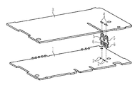
- Fig. 1 relates to an electronic circuit whose circuit elements in two in a fixed distance from each other held circuit carriers 1, 3 are arranged. For the sake of clarity, the circuit carriers 1, 3 are drawn without these circuit elements and conductor tracks.
- the exemplary arrangement comprises two electrically conductive connections between the two circuit carriers 1, 3.
- two electrical contacts of the first circuit carrier 1 are connected to two electrical contacts of the second circuit carrier 3 by means of a respective tongue 5.
- the electrical contacts of the circuit carriers 1, 3 are connected, for example, with conductor tracks or directly to terminals of circuit elements.
- the illustrated tabs 5 each comprise two terminal lugs 6, which are pressed or soldered in as plated-through holes 2 executed electrical contacts of the first circuit substrate 1.
- plated-through holes 2 executed electrical contacts of the first circuit substrate 1.
- the illustrated tabs 5 can be used, in particular those with only one terminal lug 6, which only require a through-hole 2 in the first circuit substrate 1.
- the bore 2 or the holes 2 can be executed laminated on one side and soldered with outstanding ends of the terminal lugs 6.
- the mounting of the tabs 5 takes place, for example, in such a way that the tabs 5 are placed by means of automatic assembly on the first circuit substrate 1 and that subsequently the terminal lugs 6 are fixed by means of wave soldering.
- these can also be made one-sided laminated.
- the respective tongue 5 is soldered to the solder hole surrounding the slot edge.
- the end portions of the tabs 5 are soldered into the slots 4 of the second circuit substrate 3.
- the resulting mechanical connection of the two circuit carriers 1, 3 is generally sufficiently stable, so that additional fastening means for fixed spacing of the two circuit carriers 1, 3 can be omitted. This is especially true when an arrangement comprises a plurality of tabs 5, wherein the terminal lugs 6 are soldered into the holes 2 and the end portions of the tabs 5 in the slots 4.
Landscapes
- Engineering & Computer Science (AREA)
- Manufacturing & Machinery (AREA)
- Microelectronics & Electronic Packaging (AREA)
- Coupling Device And Connection With Printed Circuit (AREA)
- Combinations Of Printed Boards (AREA)
Applications Claiming Priority (1)
| Application Number | Priority Date | Filing Date | Title |
|---|---|---|---|
| AT6612008A AT506929B1 (de) | 2008-04-29 | 2008-04-29 | Anordnung zweier schaltungsträger |
Publications (3)
| Publication Number | Publication Date |
|---|---|
| EP2113967A2 true EP2113967A2 (fr) | 2009-11-04 |
| EP2113967A3 EP2113967A3 (fr) | 2011-06-29 |
| EP2113967B1 EP2113967B1 (fr) | 2016-02-24 |
Family
ID=40643176
Family Applications (1)
| Application Number | Title | Priority Date | Filing Date |
|---|---|---|---|
| EP09153486.7A Not-in-force EP2113967B1 (fr) | 2008-04-29 | 2009-02-24 | Agencement de deux circuits imprimés |
Country Status (2)
| Country | Link |
|---|---|
| EP (1) | EP2113967B1 (fr) |
| AT (1) | AT506929B1 (fr) |
Citations (1)
| Publication number | Priority date | Publication date | Assignee | Title |
|---|---|---|---|---|
| AT500260A1 (de) | 2003-05-08 | 2005-11-15 | Siemens Ag Oesterreich | Anordnung von leiterplatten |
Family Cites Families (8)
| Publication number | Priority date | Publication date | Assignee | Title |
|---|---|---|---|---|
| US3820061A (en) * | 1972-09-05 | 1974-06-25 | Hewlett Packard Co | Connector for printed circuit boards |
| US5548486A (en) * | 1994-01-21 | 1996-08-20 | International Business Machines Corporation | Pinned module |
| US5624269A (en) * | 1995-06-07 | 1997-04-29 | Yazaki Corporation | Electrical contact terminal for printed circuit board |
| NO982678L (no) * | 1997-06-26 | 1998-12-28 | Siemens Ag | Pluggkoblingsstykke |
| US6155887A (en) * | 1999-05-27 | 2000-12-05 | Airborn, Inc. | Stackable connector system and contact for use therein |
| JP3826696B2 (ja) * | 2000-09-19 | 2006-09-27 | 日産自動車株式会社 | 配線構造 |
| DE10134380B4 (de) * | 2001-07-14 | 2020-11-12 | HELLA GmbH & Co. KGaA | Gehäuse mit darin untergebrachter elektrischer Schaltung |
| KR100704971B1 (ko) * | 2005-01-21 | 2007-04-10 | 타이코에이엠피 주식회사 | 무납땜 연결 구조를 갖는 더블 인쇄회로기판 |
-
2008
- 2008-04-29 AT AT6612008A patent/AT506929B1/de not_active IP Right Cessation
-
2009
- 2009-02-24 EP EP09153486.7A patent/EP2113967B1/fr not_active Not-in-force
Patent Citations (1)
| Publication number | Priority date | Publication date | Assignee | Title |
|---|---|---|---|---|
| AT500260A1 (de) | 2003-05-08 | 2005-11-15 | Siemens Ag Oesterreich | Anordnung von leiterplatten |
Also Published As
| Publication number | Publication date |
|---|---|
| EP2113967B1 (fr) | 2016-02-24 |
| AT506929A2 (de) | 2009-12-15 |
| AT506929B1 (de) | 2012-10-15 |
| EP2113967A3 (fr) | 2011-06-29 |
| AT506929A3 (de) | 2010-02-15 |
Similar Documents
| Publication | Publication Date | Title |
|---|---|---|
| DE69026145T2 (de) | Koaxiales Kontaktelement | |
| DE102011050921A1 (de) | Schneidklemmverbinder (LSA-Verbinder) | |
| EP2356722B1 (fr) | Connecteur enfichable pour cartes de circuits | |
| AT504960B1 (de) | Anordnung eines ersten schaltungsträgers auf einem zweiten schaltungsträger | |
| DE102021121465A1 (de) | Leiterplattenverbindungsvorrichtung und Leiterplattenanordnung | |
| WO2014068005A1 (fr) | Dispositif de contact, circuit | |
| EP2113967B1 (fr) | Agencement de deux circuits imprimés | |
| DE102005036296B4 (de) | Elektrisches Kontaktierungselement | |
| DE69702127T2 (de) | Nockenbetaetigter leiterplattenrandverbinder | |
| DE102018101792B4 (de) | Leiterkartenverbinder und dazugehörige Leiterkartenanordnung zur Übertragung hoher Stromstärken | |
| DE102012101449A1 (de) | Leiterplattenanschluss, Verfahren zur Ausbildung eines Leiterplattenanschlusses und Wechselrichter umfassend einen Leiterplattenanschluss | |
| DE69300597T2 (de) | Leiterplatten-Verbinder. | |
| DE202019003587U1 (de) | Einpress-Kontakt | |
| DE7912573U1 (de) | IC-Bauelement | |
| EP2412214B1 (fr) | Cadre de logement pour au moins une carte de circuit imprimé | |
| DE102018200682A1 (de) | Elektrische Kontaktvorrichtung sowie Schaltungsträgeranordnung | |
| EP2709212B1 (fr) | Agencement destiné à relier des plaquettes | |
| DE102012102055A1 (de) | Verbindungselement | |
| WO2022078556A1 (fr) | Procédé de fabrication d'un ensemble carte de circuit imprimé et connecteur | |
| DE10209648A1 (de) | Kontaktierungseinheit zur elektrisch leitenden Verbindung zweier elektronischer Baugruppen | |
| DE102023120885A1 (de) | Elektrischer Verbinder für ein Daten- oder Kommunikationskabel | |
| DE202022000146U1 (de) | Verbindungselement selbstverriegelnd | |
| DE102015100647B4 (de) | Leiterplatte mit Steckkontaktelement | |
| EP4336659A1 (fr) | Connecteur électrique, ensemble circuit et ensemble électrique | |
| EP0966777B1 (fr) | Ensemble electrique |
Legal Events
| Date | Code | Title | Description |
|---|---|---|---|
| PUAI | Public reference made under article 153(3) epc to a published international application that has entered the european phase |
Free format text: ORIGINAL CODE: 0009012 |
|
| AK | Designated contracting states |
Kind code of ref document: A2 Designated state(s): AT BE BG CH CY CZ DE DK EE ES FI FR GB GR HR HU IE IS IT LI LT LU LV MC MK MT NL NO PL PT RO SE SI SK TR |
|
| AX | Request for extension of the european patent |
Extension state: AL BA RS |
|
| RAP1 | Party data changed (applicant data changed or rights of an application transferred) |
Owner name: SIEMENS AKTIENGESELLSCHAFT |
|
| PUAL | Search report despatched |
Free format text: ORIGINAL CODE: 0009013 |
|
| AK | Designated contracting states |
Kind code of ref document: A3 Designated state(s): AT BE BG CH CY CZ DE DK EE ES FI FR GB GR HR HU IE IS IT LI LT LU LV MC MK MT NL NO PL PT RO SE SI SK TR |
|
| AX | Request for extension of the european patent |
Extension state: AL BA RS |
|
| 17P | Request for examination filed |
Effective date: 20111219 |
|
| AKX | Designation fees paid |
Designated state(s): AT BE BG CH CY CZ DE DK EE ES FI FR GB GR HR HU IE IS IT LI LT LU LV MC MK MT NL NO PL PT RO SE SI SK TR |
|
| RAP1 | Party data changed (applicant data changed or rights of an application transferred) |
Owner name: SIEMENS AKTIENGESELLSCHAFT |
|
| 17Q | First examination report despatched |
Effective date: 20140310 |
|
| REG | Reference to a national code |
Ref country code: DE Ref legal event code: R079 Ref document number: 502009012162 Country of ref document: DE Free format text: PREVIOUS MAIN CLASS: H01R0012320000 Ipc: H05K0001140000 |
|
| RIC1 | Information provided on ipc code assigned before grant |
Ipc: H05K 1/14 20060101AFI20150729BHEP |
|
| GRAP | Despatch of communication of intention to grant a patent |
Free format text: ORIGINAL CODE: EPIDOSNIGR1 |
|
| INTG | Intention to grant announced |
Effective date: 20150909 |
|
| GRAS | Grant fee paid |
Free format text: ORIGINAL CODE: EPIDOSNIGR3 |
|
| GRAA | (expected) grant |
Free format text: ORIGINAL CODE: 0009210 |
|
| AK | Designated contracting states |
Kind code of ref document: B1 Designated state(s): AT BE BG CH CY CZ DE DK EE ES FI FR GB GR HR HU IE IS IT LI LT LU LV MC MK MT NL NO PL PT RO SE SI SK TR |
|
| REG | Reference to a national code |
Ref country code: GB Ref legal event code: FG4D Free format text: NOT ENGLISH |
|
| REG | Reference to a national code |
Ref country code: CH Ref legal event code: EP |
|
| REG | Reference to a national code |
Ref country code: AT Ref legal event code: REF Ref document number: 777310 Country of ref document: AT Kind code of ref document: T Effective date: 20160315 |
|
| REG | Reference to a national code |
Ref country code: IE Ref legal event code: FG4D Free format text: LANGUAGE OF EP DOCUMENT: GERMAN |
|
| REG | Reference to a national code |
Ref country code: DE Ref legal event code: R096 Ref document number: 502009012162 Country of ref document: DE |
|
| REG | Reference to a national code |
Ref country code: LT Ref legal event code: MG4D |
|
| REG | Reference to a national code |
Ref country code: NL Ref legal event code: MP Effective date: 20160224 |
|
| PG25 | Lapsed in a contracting state [announced via postgrant information from national office to epo] |
Ref country code: IT Free format text: LAPSE BECAUSE OF FAILURE TO SUBMIT A TRANSLATION OF THE DESCRIPTION OR TO PAY THE FEE WITHIN THE PRESCRIBED TIME-LIMIT Effective date: 20160224 Ref country code: FI Free format text: LAPSE BECAUSE OF FAILURE TO SUBMIT A TRANSLATION OF THE DESCRIPTION OR TO PAY THE FEE WITHIN THE PRESCRIBED TIME-LIMIT Effective date: 20160224 Ref country code: GR Free format text: LAPSE BECAUSE OF FAILURE TO SUBMIT A TRANSLATION OF THE DESCRIPTION OR TO PAY THE FEE WITHIN THE PRESCRIBED TIME-LIMIT Effective date: 20160525 Ref country code: HR Free format text: LAPSE BECAUSE OF FAILURE TO SUBMIT A TRANSLATION OF THE DESCRIPTION OR TO PAY THE FEE WITHIN THE PRESCRIBED TIME-LIMIT Effective date: 20160224 Ref country code: NO Free format text: LAPSE BECAUSE OF FAILURE TO SUBMIT A TRANSLATION OF THE DESCRIPTION OR TO PAY THE FEE WITHIN THE PRESCRIBED TIME-LIMIT Effective date: 20160524 Ref country code: ES Free format text: LAPSE BECAUSE OF FAILURE TO SUBMIT A TRANSLATION OF THE DESCRIPTION OR TO PAY THE FEE WITHIN THE PRESCRIBED TIME-LIMIT Effective date: 20160224 |
|
| PG25 | Lapsed in a contracting state [announced via postgrant information from national office to epo] |
Ref country code: PT Free format text: LAPSE BECAUSE OF FAILURE TO SUBMIT A TRANSLATION OF THE DESCRIPTION OR TO PAY THE FEE WITHIN THE PRESCRIBED TIME-LIMIT Effective date: 20160624 Ref country code: NL Free format text: LAPSE BECAUSE OF FAILURE TO SUBMIT A TRANSLATION OF THE DESCRIPTION OR TO PAY THE FEE WITHIN THE PRESCRIBED TIME-LIMIT Effective date: 20160224 Ref country code: PL Free format text: LAPSE BECAUSE OF FAILURE TO SUBMIT A TRANSLATION OF THE DESCRIPTION OR TO PAY THE FEE WITHIN THE PRESCRIBED TIME-LIMIT Effective date: 20160224 Ref country code: SE Free format text: LAPSE BECAUSE OF FAILURE TO SUBMIT A TRANSLATION OF THE DESCRIPTION OR TO PAY THE FEE WITHIN THE PRESCRIBED TIME-LIMIT Effective date: 20160224 Ref country code: LV Free format text: LAPSE BECAUSE OF FAILURE TO SUBMIT A TRANSLATION OF THE DESCRIPTION OR TO PAY THE FEE WITHIN THE PRESCRIBED TIME-LIMIT Effective date: 20160224 Ref country code: LT Free format text: LAPSE BECAUSE OF FAILURE TO SUBMIT A TRANSLATION OF THE DESCRIPTION OR TO PAY THE FEE WITHIN THE PRESCRIBED TIME-LIMIT Effective date: 20160224 Ref country code: BE Free format text: LAPSE BECAUSE OF NON-PAYMENT OF DUE FEES Effective date: 20160229 |
|
| REG | Reference to a national code |
Ref country code: CH Ref legal event code: PL |
|
| PG25 | Lapsed in a contracting state [announced via postgrant information from national office to epo] |
Ref country code: CH Free format text: LAPSE BECAUSE OF NON-PAYMENT OF DUE FEES Effective date: 20160229 Ref country code: LI Free format text: LAPSE BECAUSE OF NON-PAYMENT OF DUE FEES Effective date: 20160229 Ref country code: DK Free format text: LAPSE BECAUSE OF FAILURE TO SUBMIT A TRANSLATION OF THE DESCRIPTION OR TO PAY THE FEE WITHIN THE PRESCRIBED TIME-LIMIT Effective date: 20160224 Ref country code: EE Free format text: LAPSE BECAUSE OF FAILURE TO SUBMIT A TRANSLATION OF THE DESCRIPTION OR TO PAY THE FEE WITHIN THE PRESCRIBED TIME-LIMIT Effective date: 20160224 |
|
| REG | Reference to a national code |
Ref country code: DE Ref legal event code: R097 Ref document number: 502009012162 Country of ref document: DE |
|
| PG25 | Lapsed in a contracting state [announced via postgrant information from national office to epo] |
Ref country code: RO Free format text: LAPSE BECAUSE OF FAILURE TO SUBMIT A TRANSLATION OF THE DESCRIPTION OR TO PAY THE FEE WITHIN THE PRESCRIBED TIME-LIMIT Effective date: 20160224 Ref country code: CZ Free format text: LAPSE BECAUSE OF FAILURE TO SUBMIT A TRANSLATION OF THE DESCRIPTION OR TO PAY THE FEE WITHIN THE PRESCRIBED TIME-LIMIT Effective date: 20160224 Ref country code: SK Free format text: LAPSE BECAUSE OF FAILURE TO SUBMIT A TRANSLATION OF THE DESCRIPTION OR TO PAY THE FEE WITHIN THE PRESCRIBED TIME-LIMIT Effective date: 20160224 |
|
| REG | Reference to a national code |
Ref country code: IE Ref legal event code: MM4A |
|
| PLBE | No opposition filed within time limit |
Free format text: ORIGINAL CODE: 0009261 |
|
| STAA | Information on the status of an ep patent application or granted ep patent |
Free format text: STATUS: NO OPPOSITION FILED WITHIN TIME LIMIT |
|
| GBPC | Gb: european patent ceased through non-payment of renewal fee |
Effective date: 20160524 |
|
| PG25 | Lapsed in a contracting state [announced via postgrant information from national office to epo] |
Ref country code: IE Free format text: LAPSE BECAUSE OF NON-PAYMENT OF DUE FEES Effective date: 20160224 |
|
| 26N | No opposition filed |
Effective date: 20161125 |
|
| REG | Reference to a national code |
Ref country code: FR Ref legal event code: ST Effective date: 20170109 |
|
| PG25 | Lapsed in a contracting state [announced via postgrant information from national office to epo] |
Ref country code: BG Free format text: LAPSE BECAUSE OF FAILURE TO SUBMIT A TRANSLATION OF THE DESCRIPTION OR TO PAY THE FEE WITHIN THE PRESCRIBED TIME-LIMIT Effective date: 20160524 Ref country code: SI Free format text: LAPSE BECAUSE OF FAILURE TO SUBMIT A TRANSLATION OF THE DESCRIPTION OR TO PAY THE FEE WITHIN THE PRESCRIBED TIME-LIMIT Effective date: 20160224 |
|
| REG | Reference to a national code |
Ref country code: AT Ref legal event code: MM01 Ref document number: 777310 Country of ref document: AT Kind code of ref document: T Effective date: 20160224 |
|
| PG25 | Lapsed in a contracting state [announced via postgrant information from national office to epo] |
Ref country code: FR Free format text: LAPSE BECAUSE OF NON-PAYMENT OF DUE FEES Effective date: 20160425 |
|
| PG25 | Lapsed in a contracting state [announced via postgrant information from national office to epo] |
Ref country code: GB Free format text: LAPSE BECAUSE OF NON-PAYMENT OF DUE FEES Effective date: 20160524 Ref country code: AT Free format text: LAPSE BECAUSE OF NON-PAYMENT OF DUE FEES Effective date: 20160224 |
|
| PGFP | Annual fee paid to national office [announced via postgrant information from national office to epo] |
Ref country code: DE Payment date: 20170419 Year of fee payment: 9 |
|
| PG25 | Lapsed in a contracting state [announced via postgrant information from national office to epo] |
Ref country code: MT Free format text: LAPSE BECAUSE OF FAILURE TO SUBMIT A TRANSLATION OF THE DESCRIPTION OR TO PAY THE FEE WITHIN THE PRESCRIBED TIME-LIMIT Effective date: 20160224 |
|
| PG25 | Lapsed in a contracting state [announced via postgrant information from national office to epo] |
Ref country code: MC Free format text: LAPSE BECAUSE OF FAILURE TO SUBMIT A TRANSLATION OF THE DESCRIPTION OR TO PAY THE FEE WITHIN THE PRESCRIBED TIME-LIMIT Effective date: 20160224 |
|
| PG25 | Lapsed in a contracting state [announced via postgrant information from national office to epo] |
Ref country code: HU Free format text: LAPSE BECAUSE OF FAILURE TO SUBMIT A TRANSLATION OF THE DESCRIPTION OR TO PAY THE FEE WITHIN THE PRESCRIBED TIME-LIMIT; INVALID AB INITIO Effective date: 20090224 Ref country code: CY Free format text: LAPSE BECAUSE OF FAILURE TO SUBMIT A TRANSLATION OF THE DESCRIPTION OR TO PAY THE FEE WITHIN THE PRESCRIBED TIME-LIMIT Effective date: 20160224 |
|
| PG25 | Lapsed in a contracting state [announced via postgrant information from national office to epo] |
Ref country code: IS Free format text: LAPSE BECAUSE OF FAILURE TO SUBMIT A TRANSLATION OF THE DESCRIPTION OR TO PAY THE FEE WITHIN THE PRESCRIBED TIME-LIMIT Effective date: 20160224 Ref country code: LU Free format text: LAPSE BECAUSE OF NON-PAYMENT OF DUE FEES Effective date: 20160224 Ref country code: TR Free format text: LAPSE BECAUSE OF FAILURE TO SUBMIT A TRANSLATION OF THE DESCRIPTION OR TO PAY THE FEE WITHIN THE PRESCRIBED TIME-LIMIT Effective date: 20160224 Ref country code: MK Free format text: LAPSE BECAUSE OF FAILURE TO SUBMIT A TRANSLATION OF THE DESCRIPTION OR TO PAY THE FEE WITHIN THE PRESCRIBED TIME-LIMIT Effective date: 20160224 |
|
| REG | Reference to a national code |
Ref country code: DE Ref legal event code: R119 Ref document number: 502009012162 Country of ref document: DE |
|
| PG25 | Lapsed in a contracting state [announced via postgrant information from national office to epo] |
Ref country code: DE Free format text: LAPSE BECAUSE OF NON-PAYMENT OF DUE FEES Effective date: 20180901 |