EP2115435B1 - Procédé et agencement pour la détection de défauts mécaniques d'un composant semi-conducteur, notamment d'une pile solaire ou d'un agencement de piles solaires - Google Patents
Procédé et agencement pour la détection de défauts mécaniques d'un composant semi-conducteur, notamment d'une pile solaire ou d'un agencement de piles solaires Download PDFInfo
- Publication number
- EP2115435B1 EP2115435B1 EP08706845.8A EP08706845A EP2115435B1 EP 2115435 B1 EP2115435 B1 EP 2115435B1 EP 08706845 A EP08706845 A EP 08706845A EP 2115435 B1 EP2115435 B1 EP 2115435B1
- Authority
- EP
- European Patent Office
- Prior art keywords
- radiation
- semiconductor
- semiconductor layer
- semiconductor device
- mechanical defects
- Prior art date
- Legal status (The legal status is an assumption and is not a legal conclusion. Google has not performed a legal analysis and makes no representation as to the accuracy of the status listed.)
- Active
Links
Images


Classifications
-
- G—PHYSICS
- G01—MEASURING; TESTING
- G01N—INVESTIGATING OR ANALYSING MATERIALS BY DETERMINING THEIR CHEMICAL OR PHYSICAL PROPERTIES
- G01N21/00—Investigating or analysing materials by the use of optical means, i.e. using sub-millimetre waves, infrared, visible or ultraviolet light
- G01N21/62—Systems in which the material investigated is excited whereby it emits light or causes a change in wavelength of the incident light
- G01N21/66—Systems in which the material investigated is excited whereby it emits light or causes a change in wavelength of the incident light electrically excited, e.g. electroluminescence
-
- G—PHYSICS
- G01—MEASURING; TESTING
- G01N—INVESTIGATING OR ANALYSING MATERIALS BY DETERMINING THEIR CHEMICAL OR PHYSICAL PROPERTIES
- G01N21/00—Investigating or analysing materials by the use of optical means, i.e. using sub-millimetre waves, infrared, visible or ultraviolet light
- G01N21/84—Systems specially adapted for particular applications
- G01N21/88—Investigating the presence of flaws or contamination
- G01N21/95—Investigating the presence of flaws or contamination characterised by the material or shape of the object to be examined
- G01N21/9501—Semiconductor wafers
- G01N21/9505—Wafer internal defects, e.g. microcracks
-
- H—ELECTRICITY
- H02—GENERATION; CONVERSION OR DISTRIBUTION OF ELECTRIC POWER
- H02S—GENERATION OF ELECTRIC POWER BY CONVERSION OF INFRARED RADIATION, VISIBLE LIGHT OR ULTRAVIOLET LIGHT, e.g. USING PHOTOVOLTAIC [PV] MODULES
- H02S50/00—Monitoring or testing of PV systems, e.g. load balancing or fault identification
- H02S50/10—Testing of PV devices, e.g. of PV modules or single PV cells
Definitions
- the present invention relates to a method for detecting mechanical defects of a semiconductor component, in particular a solar cell or solar cell arrangement, according to claim 1 and a corresponding arrangement according to claim 11, as well as the use according to claim 14.
- the EP 1 416 288 B1 describes a method for the optical detection of mechanical defects in semiconductor components, in particular solar cell arrangements that have at least one pn junction and at least one semiconductor layer made of a semiconductor material with a direct band transition.
- the active radiation behavior is influenced, which can then be evaluated for the detection of mechanical defects.
- the component is not passively irradiated, but rather the radiation behavior of the component itself is actively stimulated.
- the radiation behavior is influenced by the radiative recombination of charge carriers induced in the pn junction polarized in the forward direction at the direct band transition, which according to the EP 1 416 288 B1 In the case of semiconductor material such as germanium with an indirect band transition, this is not possible because there is no sufficient radiative recombination of charge carriers in it.
- This object is achieved by a method for detecting mechanical defects in a semiconductor component, in particular a solar cell or solar cell arrangement, with the features of claim 1 and by a corresponding arrangement with the features of claim 11.
- the present invention is based on the knowledge that indirect semiconductors such as silicon also have an evaluable radiation behavior under certain conditions. From the publication " Photographic surveying of minority carrier diffusion length in polycrystalline silicon solar cells by electroluminescence ", T. Fuyuki, H. Kondo, T. Yamazaki, Y. Takahashi and Y. Uraoka, Appl. Phys. Lett. 86, 262108, 2005 , shows that the minority carrier diffusion length in polycrystalline silicon can be determined on the basis of electroluminescence and thus indirect semiconductors also emit sufficient evaluable electroluminescence. According to the invention, this knowledge is now used to make the from EP 1 416 288 B1 to be able to use known methods by appropriate modification also for the detection of mechanical defects in semiconductor components with indirect semiconductor material.
- an infrared filter can do everything visible light are masked out, whereby relatively less sensitive detectors can be used and the defect detection under ambient light is possible.
- suitable (bandpass) filters can be used to isolate the radiation from a specific pn junction and only check these semiconductor layers for defects.
- optical detection is to be understood in particular as the spatial resolution of the detection of the electromagnetic radiation emitted by the semiconductor component.
- the radiation behavior is analyzed in such a way that the radiation behavior of the semiconductor layer is examined for abrupt, essentially one-dimensional changes in intensity along the semiconductor layer and the detected changes in intensity are identified as mechanical defects in the semiconductor component.
- Such an analysis can be carried out automatically by appropriate image processing systems or radiation intensity detectors.
- the global radiation behavior is not only considered qualitatively here (radiation present or not present), but the intensity profile of the radiation behavior along the component or along the semiconductor layer with an indirect band transition is examined locally. In this way, local defects can be detected which impair the functionality of the component in certain subregions or can interfere in some other way.
- An abrupt, essentially one-dimensionally extended change in intensity suggests a mechanical defect such as a break in a semiconductor layer.
- the method can also be used to detect local cloudiness, degradation or the like, for example in cover glasses and cover layers of solar cells or the like.
- these can then have an effect, for example, as a two-dimensional change in intensity in the radiation behavior and can be detected accordingly.
- the present invention offers the advantage that a significant improvement in the detection of mechanical defects in planar semiconductor components is possible, which in particular consist of a semiconductor material with an indirect band transition such as silicon. Compared to the visual cell inspection, which reaches its limits, especially with textured silicon solar cells, errors can be detected almost 100% (compared to a visual detection rate of usually less than 50%). Furthermore, the inspection is person-independent and reproducible and enables clear error documentation. In addition, the process saves time and can be automated.
- a shadowing of direct incident light on a surface of the semiconductor component can take place during optical detection.
- This offers the advantage that only electromagnetic radiation is detected and evaluated which is emitted by the semiconductor component to which the forward voltage is applied. Electromagnetic radiation reflected by the component, which is generated, for example, by light incident laterally on the surface of the semiconductor component, can thereby be avoided.
- the optical detection can take place within a time span of at most two seconds. It has been shown that such a time span for recording high-resolution images of the Si-based semiconductor component is suitable for further evaluation for detection by means of a conventional Si-CCD camera.
- a voltage can also be applied to operate the pn junction in the forward direction, which voltage causes a current in a range of one to two times a short-circuit current intensity of the semiconductor component.
- a range for recording high-resolution images of the Si-based semiconductor component is suitable for further evaluation for detection by means of a conventional Si-CCD camera.
- the semiconductor material with an indirect band transition can comprise silicon, in particular polycrystalline silicon.
- an indirect detection of mechanical defects of a radiation-inactive layer of the semiconductor component can take place, the radiation behavior of an adjacent radiation-active semiconductor layer being automatically examined for abrupt, essentially one-dimensionally extended intensity changes along the semiconductor layer and detected intensity changes as mechanical defects the radiation-inactive layer of the semiconductor component can be identified.
- an embodiment of the present invention can also detect a breakage or degradation of a non-radiating layer of the semiconductor component using the approach according to the invention, since the radiation behavior of the Semiconductor component is also influenced by this breakage or the degradations in the non-radiative layer.
- a combined detection of mechanical defects and detection of the electrical effects of the mechanical defects can take place, with an analysis of the radiation behavior of the component in a first wavelength range of the detection of mechanical defects and an analysis of the radiation behavior of the component in a second wavelength range the recording of the electrical effects is taken as a basis.
- a plurality of n semiconductor components can be arranged in a series connection and / or parallel connection on a common component carrier and a voltage which is n times the value in series connection can be applied to the entirety of the semiconductor components corresponds to the voltage and, in parallel connection, the n-fold current for operating a component in the forward direction.
- a voltage which is n times the value in series connection can be applied to the entirety of the semiconductor components corresponds to the voltage and, in parallel connection, the n-fold current for operating a component in the forward direction.
- the device for optical detection further comprises a device for shading direct incident light on a surface of the semiconductor component, since the detection of the radiation emitted by the semiconductor component can be negatively influenced by reflections of light incident laterally on a surface of the semiconductor component.
- the device for optical detection can also be designed to carry out the optical detection within a time span of at most two seconds.
- the voltage supply can be designed to apply a voltage for operating the pn junction in the forward direction via the voltage supply connections, which voltage causes a current in a range of approximately one to two times a short-circuit current intensity of the semiconductor component.
- Fig. 1 a diagram of a basic structure for the detection of mechanical defects in a semiconductor component according to an embodiment of the present invention is shown.
- Fig. 1 shows a semiconductor component 10, which comprises an upper electrode 12, a lower electrode 14 and a semiconductor material 16 lying in between.
- the semiconductor material 16 can be a semiconductor material with an indirect band transition such as silicon (Si) or germanium (Ge).
- Si silicon
- Ge germanium
- an n-doped layer 18 is arranged over a p-doped layer 20. This forms a pn junction 22.
- Fig. 1 shows a diagram of a basic structure for the detection of mechanical defects in a semiconductor component according to an embodiment of the present invention.
- Fig. 1 shows a semiconductor component 10, which comprises an upper electrode 12, a lower electrode 14 and a semiconductor material 16 lying in between.
- the semiconductor material 16 can be a semiconductor material with an indirect band transition such as silicon (Si) or germanium (Ge).
- an n-doped layer 18 is
- a voltage V 23 can be applied between the upper electrode 12 and the lower electrode 14.
- a recording unit 24 which has, for example, an infrared filter 26, an optical sensor such as a CCD camera 28 (with an upstream optics) and an image evaluation unit 30 connected to the optical sensor (CCD camera) 28.
- Fig. 1 lateral shutters 32 which are configured to shield lateral light 34 from a surface of the semiconductor device 10 (i.e., for example, from the upper surface of the upper electrode 12).
- a solar cell arrangement is now used for the semiconductor component 10, a technical effect can be used according to which a solar cell not only generates electricity when light falls, but also emits electromagnetic radiation (or electroluminescence occurs) when a voltage 23 is applied between the upper electrode 12 and the lower electrode 14 in such a way that the pn junction 22 is operated in the forward direction.
- This effect occurs mainly when using semiconductor materials with a direct band transition (radiating recombination of the charge carriers), but it was also found that in materials with an indirect band transition a (much weaker) electroluminescence occurs, the intensity of which is proportional to the minority carrier diffusion length.
- breaks or defects in the semiconductor component also influence the minority carrier diffusion length.
- breaks or defects act as current sinks and, in connection with the transverse conductivity of the cell, macroscopically influence the lateral current distribution and thus the spatial distribution of the electroluminescence of the cell, as in the publication " Utilizing lateral current spreading in multijunction solar cells: An alternative approach to detecting mechanical defects ", CG Zimmermann, J. Appl. Phys. 100, 023714, 2006 shown.
- breaks or defects can be inferred.
- this electroluminescence occurs in the infrared spectral range (ie electromagnetic radiation with a wavelength of more than 800 nm).
- an infrared filter 26 is used in the recording unit 24 to reduce the sensitivity of the recording sensor 28, which is, for example, as shown in FIG Fig. 1 a conventional Si-CCD camera can be shown, specifically to focus on the spectral range of interest and to hide the other disruptive spectral ranges.
- the side screens 32 then prevent the infrared portion of the laterally incident light 34 from being reflected from the surface of the semiconductor component 10 into the recording unit 28, which would cause the recorded image to be falsified.
- the recording unit 28 can optionally also be provided with other filter combinations in order to selectively detect the electroluminescence of one or more pn transitions.
- Fig. 2 shows a schematic representation of how a recording of the in Fig. 1 surface of the semiconductor component 10 shown could look like.
- the break 46 in the pn junction 22 emerges clearly recognizable as an essentially one-dimensional decrease in intensity of the electroluminescent radiation of the cell (light areas 40).
- the break is shown accordingly as a black line.
- the break 46 runs in a (non-active) layer arranged below the pn junction 22 and this break has a negative effect on the crystal structure in the pn junction 22, so that a break in one does not -active layer can be detected with the proposed approach.
- These abrupt, essentially one-dimensional changes in intensity very easily allow defects to be automatically recognized by current image processing systems.
- the method proposed here also enables the electrical effects associated with a break to be detected.
- the entire area 42 is electrically impaired by the break and is characterized by reduced electroluminescence.
- area 44 this is only the case for the area below the break 46.
- the radiation behavior of the solar cell arrangement can be optically analyzed in a simple manner, so that direct, unambiguous and reproducible conclusions can be drawn about defects in the solar cell arrangement.
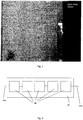
- Fig. 3 represents an exemplary photo of such an electroluminescent image of a silicon solar cell, in which a corresponding voltage was applied to operate the respective pn junctions in the forward direction.
- I 1500 mA
- t 2 s.
- FIG. 4 shows a plurality of solar cell arrangements 50 combined to form a string, each of which consists, for example, of a semiconductor component 10, as shown in FIG Fig. 1 is shown.
- the individual solar cell arrangements 20 are connected in series via their electrodes 51a and 51b.
- the solar cell arrangements 50 are applied to a common carrier 52. If a voltage is now applied to this entire string which, with n solar cell arrangement 50, is n times the voltage in order to switch a solar cell arrangement 50 in the forward direction, then the entire string of solar cells can be tested in one operation.
- Fig. 5 shows schematically a circuit diagram with the essential functionalities of a possible embodiment of the image processing unit 30 in detail.
- This image processing unit 30 has an image data storage area 60 for storing a radiation image of the semiconductor layer 10 (or the pn junction 22), a program storage area 62 containing an image processing program designed to automatically examine the radiation image for abrupt, essentially one-dimensional changes in intensity Identification of the detected changes in intensity as mechanical defects of the semiconductor component and a second program memory area 64 containing a program for analyzing the radiation image on the electrical effects of the mechanical defects.
- the two programs can be executed by a computer unit 66 which is connected to the individual memory areas 60 to 64 in terms of data technology.
- Fig. 6 shows a flow chart of an embodiment of the method according to the invention.
- a voltage is applied to a pn junction of the semiconductor component (with at least one pn junction in a semiconductor material with an indirect band transition) in the forward direction of the pn junction.
- the radiation behavior of the semiconductor layer generated by the applied voltage in the case of a Si semiconductor component is filtered at least for partial areas of the semiconductor layer by means of an infrared filter in such a way that electromagnetic radiation in the spectral range with a wavelength lower than infrared is blocked.
- an infrared filter in such a way that electromagnetic radiation in the spectral range with a wavelength lower than infrared is blocked.
- other filter combinations can be useful.
- the filtered radiation behavior is then optically recorded in a third method step 74, for example by means of a CCD camera.
- the detected radiation behavior is evaluated in a final method step 76a, the radiation behavior of the semiconductor layer being automatically examined for abrupt, essentially one-dimensional changes in intensity along the semiconductor layer and detected changes in intensity being identified as mechanical defects in the semiconductor component (method step 78).
- the integral over the radiation intensity of at least a first partial region of a first semiconductor layer can be determined automatically, then the integral over the radiation intensity of at least one comparison region of the same semiconductor layer or a second semiconductor layer can be determined and based on the result of an automatic comparison of the two Integrals of the first sub-area are identified as defective or as free from defects (method step 78).
- a conventional CCD camera such as the commercially available Si-CCD camera Sony XCD-SX910
- the selected parameters enable good compatibility of the process with the requirements of production: the selected current range is uncritical for the cell and does not damage it.
- the exposure times of 1-2 s ensure a quick inspection of all cells.
- the camera uses a standard Si-CCD detector and is therefore inexpensive, especially since no additional measures, such as cooling the camera, are required. Visible ambient light is blocked by the infrared filter, only shading from direct incident light on the cell can take place.
Landscapes
- Health & Medical Sciences (AREA)
- Biochemistry (AREA)
- Physics & Mathematics (AREA)
- Life Sciences & Earth Sciences (AREA)
- Chemical & Material Sciences (AREA)
- Analytical Chemistry (AREA)
- General Health & Medical Sciences (AREA)
- General Physics & Mathematics (AREA)
- Immunology (AREA)
- Pathology (AREA)
- Nuclear Medicine, Radiotherapy & Molecular Imaging (AREA)
- Photovoltaic Devices (AREA)
- Investigating Materials By The Use Of Optical Means Adapted For Particular Applications (AREA)
Claims (14)
- Procédé de détection de défauts mécaniques d'un composant semi-conducteur (10) à base de silicium ou de germanium, en particulier d'une cellule solaire ou d'un ensemble de cellules solaires, comportant au moins une jonction pn (22) dans une couche semi-conductrice d'un matériau semi-conducteur (16) à transition inter-bandes indirecte, dans lequel- une tension (23) est appliquée (70) à ladite au moins une jonction pn (22) pour faire fonctionner la jonction pn (22) dans le sens direct,- le comportement de rayonnement de la couche semi-conductrice produit par la tension appliquée (23) est détecté optiquement (74) et évalué (76) au moins pour des zones partielles de la couche semi-conductrice,dans lequel le comportement de rayonnement de la couche semi-conductrice est inspecté automatiquement (76a) en ce qui concerne des variations d'intensité abruptes, d'extension essentiellement unidimensionnelle le long de la couche semi-conductrice, et les variations d'intensité détectées sont caractérisées (78) comme des défauts mécaniques (46) du composant semi-conducteur (10),
caractérisé en ce qu'un filtre infrarouge (26) est utilisé (72) pour la détection optique du comportement de rayonnement de la couche semi-conductrice, de telle sorte qu'un rayonnement électromagnétique dans le domaine spectral ayant une longueur d'onde inférieure à l'infrarouge est bloqué, et/ou que l'électroluminescence d'une ou de plusieurs jonctions pn est sélectionnée au moyen de combinaisons de filtres adaptées au matériau semi-conducteur. - Procédé selon la revendication 1,
caractérisé en ce que l'intégrale sur l'intensité de rayonnement d'au moins une première zone partielle (44, 42) d'une première couche semi-conductrice est déterminée automatiquement, ensuite l'intégrale sur l'intensité de rayonnement d'au moins une zone de comparaison de la même couche semi-conductrice (44, 42) ou d'une deuxième couche semi-conductrice (42, 40) est déterminée (76b) et, sur la base du résultat d'une comparaison automatique des deux intégrales, la première zone partielle (44) est caractérisée (78) comme étant défectueuse ou sans défaut. - Procédé selon l'une des revendications 1 ou 2,
caractérisé en ce que lors de la détection optique (74), une occultation de la lumière incidente directe (34) sur une surface du composant semi-conducteur (10) est effectuée. - Procédé selon l'une des revendications 1 à 3,
caractérisé en ce que la détection optique (74) a lieu dans un intervalle de temps de deux secondes au maximum. - Procédé selon l'une des revendications 1 à 4,
caractérisé en ce que pour faire fonctionner la jonction pn (22) dans le sens direct, on applique une tension (23) qui provoque un courant dans une plage d'environ une à deux fois une intensité du courant de court-circuit du composant semi-conducteur (10). - Procédé selon l'une des revendications 1 à 5,
caractérisé en ce que le matériau semi-conducteur (16) à transition inter-bandes indirecte comprend du silicium, en particulier du silicium polycristallin. - Procédé selon l'une des revendications 1 à 6,
caractérisé en ce qu'une détection indirecte de défauts mécaniques d'une couche inactive au rayonnement du composant semi-conducteur (10) est effectuée, dans lequel le comportement au rayonnement d'une couche semi-conductrice active au rayonnement adjacente est inspecté automatiquement en ce qui concerne des variations d'intensité abruptes, d'extension essentiellement unidimensionnelle le long de la couche semi-conductrice et les variations d'intensité détectées sont caractérisées comme des défauts mécaniques (46) de la couche inactive au rayonnement du composant semi-conducteur (10). - Procédé selon l'une des revendications 1 à 7,
caractérisé en ce qu'une détection combinée de défauts mécaniques (46) et des effets électriques des défauts mécaniques est effectuée, dans lequel une analyse du comportement de rayonnement du composant semi-conducteur (10) dans une première plage de longueurs d'onde est utilisée comme base pour la détection de défauts mécaniques et une analyse du comportement de rayonnement du composant semi-conducteur (10) dans une deuxième plage de longueurs d'onde est utilisée comme base pour la détection des effets électriques. - Procédé selon l'une des revendications 1 à 8,
caractérisé en ce qu'une pluralité de n composants semi-conducteurs (50, 10) est disposée en série sur un support de composants commun (52) et une tension correspondant à n fois la tension (23) pour faire fonctionner un composant semi-conducteur (10) dans le sens direct est appliquée à la totalité des composants semi-conducteurs (50, 10). - Procédé selon l'une des revendications 1 à 8,
caractérisé en ce qu'une pluralité de n composants semi-conducteurs (10) est disposée en parallèle sur un support de composants commun et une tension qui provoque n fois le courant pour faire fonctionner un composant semi-conducteur (10) dans le sens direct est appliquée à la totalité des composants semi-conducteurs (10). - Ensemble pour mettre en œuvre le procédé selon l'une des revendications 1 à 10 pour la détection de défauts mécaniques d'un composant semi-conducteur (10) à base de silicium ou de germanium, en particulier d'une cellule solaire ou d'un ensemble de cellules solaires, comportant au moins une jonction pn (22) dans une couche semi-conductrice d'un matériau semi-conducteur (16) à transition inter-bandes indirecte et au moins une électrode (14) qui est reliée à la zone de type p (20) du composant semi-conducteur (10) et au moins une électrode (12) qui est reliée à la zone de type n (18) du composant semi-conducteur (10), comprenant :- des bornes d'alimentation en tension qui sont reliées aux électrodes (12, 14) du composant semi-conducteur (10) pour permettre une alimentation en tension (V, 23) pour faire fonctionner la jonction pn (22) dans le sens direct,- un dispositif (24) de détection optique et d'évaluation du comportement de rayonnement de la couche semi-conductrice qui est produit par une tension appliquée, au moins pour des zones partielles de la couche semi-conductrice, une zone de mémoire de données d'image (60) pour mémoriser une image de rayonnement de la couche semi-conductrice,- une première zone de mémoire de programme (62) contenant un programme de traitement d'image conçu pour inspecter automatiquement l'image de rayonnement en ce qui concerne des variations d'intensité abruptes, d'extension essentiellement unidimensionnelle, et pour caractériser les variations d'intensité détectées comme des défauts mécaniques (46) du composant semi-conducteur (10), et- une deuxième zone de mémoire de programme (64) contenant un programme conçu pour analyser l'image de rayonnement en ce qui concerne les effets électriques des défauts mécaniques,dans lequel le dispositif (24) de détection optique et d'évaluation du comportement du rayonnement de la couche semi-conductrice produit par une tension appliquée comprend une unité de filtrage (26),
caractérisé en ce que l'unité de filtrage est conçue de telle sorte qu'un rayonnement électromagnétique dans le domaine spectral ayant une longueur d'onde inférieure à l'infrarouge soit bloqué et/ou est conçue de telle sorte que le rayonnement d'une ou de plusieurs jonctions pn soit isolé,
en ce que le dispositif (24) de détection optique comprend un dispositif (34) pour occulter la lumière incidente directe sur une surface du composant semi-conducteur, et
en ce que le dispositif (24) de détection optique et d'évaluation est conçu de manière à détecter le comportement de rayonnement de la couche semi-conductrice d'un matériau semi-conducteur à transition inter-bandes indirecte. - Ensemble selon la revendication 11,
caractérisé en ce que le dispositif (24) de détection optique est conçu pour effectuer la détection optique dans un intervalle de temps de deux secondes au maximum. - Ensemble selon l'une des revendications 11 ou 12,
caractérisé en ce que l'alimentation en tension (V, 23) est conçue pour appliquer, par l'intermédiaire des bornes d'alimentation en tension, une tension (23) pour faire fonctionner la jonction pn (22) dans le sens direct, qui provoque un courant dans une plage d'environ une à deux fois une intensité du courant de court-circuit du composant semi-conducteur (10). - Utilisation d'un ensemble selon l'une des revendications 11 à 13 pour mettre en œuvre le procédé selon l'une des revendications 1 à 10 pour la détection de défauts mécaniques d'un composant semi-conducteur, en particulier pour la détection automatique de défauts mécaniques d'ensembles de cellules solaires.
Priority Applications (1)
| Application Number | Priority Date | Filing Date | Title |
|---|---|---|---|
| EP19162255.4A EP3514523B1 (fr) | 2007-02-09 | 2008-02-01 | Procédé pour la détection de défauts mécaniques d'un composant semi-conducteur, notamment d'une pile solaire ou d'un agencement de piles solaires |
Applications Claiming Priority (2)
| Application Number | Priority Date | Filing Date | Title |
|---|---|---|---|
| DE102007007140A DE102007007140B4 (de) | 2007-02-09 | 2007-02-09 | Verfahren und Anordnung zur Detektion mechanischer Defekte eines Halbleiter-Bauelements, insbesondere einer Solarzelle oder Solarzellen-Anordnung |
| PCT/DE2008/000180 WO2008095467A1 (fr) | 2007-02-09 | 2008-02-01 | Procédé et agencement pour la détection de défauts mécaniques d'un composant semi-conducteur, notamment d'une pile solaire ou d'un agencement de piles solaires |
Related Child Applications (2)
| Application Number | Title | Priority Date | Filing Date |
|---|---|---|---|
| EP19162255.4A Division EP3514523B1 (fr) | 2007-02-09 | 2008-02-01 | Procédé pour la détection de défauts mécaniques d'un composant semi-conducteur, notamment d'une pile solaire ou d'un agencement de piles solaires |
| EP19162255.4A Division-Into EP3514523B1 (fr) | 2007-02-09 | 2008-02-01 | Procédé pour la détection de défauts mécaniques d'un composant semi-conducteur, notamment d'une pile solaire ou d'un agencement de piles solaires |
Publications (2)
| Publication Number | Publication Date |
|---|---|
| EP2115435A1 EP2115435A1 (fr) | 2009-11-11 |
| EP2115435B1 true EP2115435B1 (fr) | 2021-05-05 |
Family
ID=39345425
Family Applications (2)
| Application Number | Title | Priority Date | Filing Date |
|---|---|---|---|
| EP08706845.8A Active EP2115435B1 (fr) | 2007-02-09 | 2008-02-01 | Procédé et agencement pour la détection de défauts mécaniques d'un composant semi-conducteur, notamment d'une pile solaire ou d'un agencement de piles solaires |
| EP19162255.4A Active EP3514523B1 (fr) | 2007-02-09 | 2008-02-01 | Procédé pour la détection de défauts mécaniques d'un composant semi-conducteur, notamment d'une pile solaire ou d'un agencement de piles solaires |
Family Applications After (1)
| Application Number | Title | Priority Date | Filing Date |
|---|---|---|---|
| EP19162255.4A Active EP3514523B1 (fr) | 2007-02-09 | 2008-02-01 | Procédé pour la détection de défauts mécaniques d'un composant semi-conducteur, notamment d'une pile solaire ou d'un agencement de piles solaires |
Country Status (4)
| Country | Link |
|---|---|
| US (1) | US8306309B2 (fr) |
| EP (2) | EP2115435B1 (fr) |
| DE (1) | DE102007007140B4 (fr) |
| WO (1) | WO2008095467A1 (fr) |
Families Citing this family (12)
| Publication number | Priority date | Publication date | Assignee | Title |
|---|---|---|---|---|
| JP4153021B1 (ja) * | 2007-10-22 | 2008-09-17 | 日清紡績株式会社 | 太陽電池の検査装置 |
| WO2010039500A2 (fr) * | 2008-09-23 | 2010-04-08 | Applied Materials, Inc. | Système d’éclairage prolongé et procédé d’essai pour des piles solaires |
| KR101055790B1 (ko) | 2009-04-17 | 2011-08-09 | 주식회사 맥사이언스 | 태양전지 교류 전계발광 화상검사 장치 |
| DE102009039399A1 (de) * | 2009-08-31 | 2011-03-03 | Fraunhofer-Gesellschaft zur Förderung der angewandten Forschung e.V. | Verfahren zur Vermessung einer Halbleiterstruktur, welche eine Solarzelle oder eine Vorstufe einer Solarzelle ist |
| EP2378278B1 (fr) * | 2010-04-19 | 2018-03-28 | Airbus Defence and Space GmbH | Procédé de criblage de cellules solaires à plusieurs jonctions |
| EP2410319A1 (fr) | 2010-07-23 | 2012-01-25 | Solarpower GmbH | Procédé et système de détection de modules solaires défectueux |
| FR2994264B1 (fr) | 2012-08-02 | 2014-09-12 | Centre Nat Rech Scient | Procede d'analyse de la structure cristalline d'un materiau semi-conducteur poly-cristallin |
| DE102012107316B4 (de) * | 2012-08-09 | 2019-08-14 | Solarzentrum Stuttgart GmbH | Verfahren und Vorrichtung zum Prüfen von Photovoltaikmodulen |
| US9666059B2 (en) * | 2014-04-01 | 2017-05-30 | Ford Global Technologies, Llc | Vehicle light anomaly state warning |
| US10361655B2 (en) * | 2016-09-07 | 2019-07-23 | Institute of Nuclear Energy Research, Atomic Energy Council, Executive Yuan, R.O.C. | Electrical inspection method for solar cells |
| JP2020129858A (ja) * | 2019-02-07 | 2020-08-27 | 株式会社トーエネック | 太陽電池の異常診断用カメラ装置およびこれを備える太陽電池の異常診断装置 |
| CN116936394B (zh) * | 2023-07-27 | 2024-02-02 | 江苏森标科技有限公司 | 一种电池片缺陷检测及颜色分选机构 |
Family Cites Families (15)
| Publication number | Priority date | Publication date | Assignee | Title |
|---|---|---|---|---|
| US5334844A (en) * | 1993-04-05 | 1994-08-02 | Space Systems/Loral, Inc. | Optical illumination and inspection system for wafer and solar cell defects |
| DE19914115A1 (de) * | 1998-04-20 | 1999-11-04 | Gfai Ges Zur Foerderung Angewa | Verfahren und System zur Fehleranalyse bei polykristallinen Wafern, Solarzellen und Solarmodulen, insbesondere zur Bestimmung der prozeß- und strukturbedingten mechanischen Spannungen |
| US6236044B1 (en) * | 1998-08-21 | 2001-05-22 | Trw Inc. | Method and apparatus for inspection of a substrate by use of a ring illuminator |
| JP4059463B2 (ja) * | 1998-12-10 | 2008-03-12 | 株式会社島津製作所 | 放射線検出装置 |
| US6225640B1 (en) * | 1999-05-19 | 2001-05-01 | Hughes Electronics Corporation | Method for electrical shunt detection and removal on semiconductors |
| US6433867B1 (en) * | 2000-01-11 | 2002-08-13 | The Aerospace Corporation | Contrast imaging method for inspecting specular surface devices |
| US6727501B1 (en) * | 2001-09-27 | 2004-04-27 | Kla-Tencor Corporation | Method for detecting over-etch defects |
| DE10248504B4 (de) * | 2002-10-13 | 2008-01-10 | Hahn-Meitner-Institut Berlin Gmbh | Zerstörungsfreies Analyseverfahren zur Güteermittlung einer Solarzelle auf Chalkopyritbasis |
| EP1416288B1 (fr) * | 2002-10-23 | 2005-03-02 | EADS Astrium GmbH | Procédé et dispositif de détection optique des défauts mécaniques dans des dispositifs à semi-conducteur, notamment pour systèmes de cellules solaires |
| CN1203281C (zh) | 2002-11-02 | 2005-05-25 | 海尔集团公司 | 挂壁式空调器室内机 |
| US20050252545A1 (en) * | 2004-05-12 | 2005-11-17 | Spire Corporation | Infrared detection of solar cell defects under forward bias |
| JP4683869B2 (ja) * | 2004-07-08 | 2011-05-18 | 独立行政法人理化学研究所 | 半導体デバイスの故障診断方法と装置 |
| US7601941B2 (en) * | 2004-11-30 | 2009-10-13 | National University Corporation NARA Institute of Science and Technology | Method and apparatus for evaluating solar cell and use thereof |
| DE102005002651B3 (de) * | 2005-01-19 | 2006-08-24 | Bundesrepublik Deutschland, vertreten durch das Bundesministerium für Wirtschaft und Arbeit, dieses vertreten durch den Präsidenten der Physikalisch-Technischen Bundesanstalt Braunschweig und Berlin | Verfahren und Vorrichtung zur Detektion von Defekten an Solarzellenelementen |
| CN103185854B (zh) * | 2006-05-05 | 2015-07-01 | Bt成像股份有限公司 | 利用发光成像测试间接带隙半导体器件的方法和系统 |
-
2007
- 2007-02-09 DE DE102007007140A patent/DE102007007140B4/de active Active
-
2008
- 2008-02-01 EP EP08706845.8A patent/EP2115435B1/fr active Active
- 2008-02-01 US US12/526,435 patent/US8306309B2/en active Active
- 2008-02-01 EP EP19162255.4A patent/EP3514523B1/fr active Active
- 2008-02-01 WO PCT/DE2008/000180 patent/WO2008095467A1/fr not_active Ceased
Also Published As
| Publication number | Publication date |
|---|---|
| US20100150428A1 (en) | 2010-06-17 |
| EP3514523A1 (fr) | 2019-07-24 |
| EP3514523B1 (fr) | 2022-10-19 |
| DE102007007140A1 (de) | 2008-08-21 |
| US8306309B2 (en) | 2012-11-06 |
| WO2008095467A1 (fr) | 2008-08-14 |
| DE102007007140B4 (de) | 2009-01-29 |
| EP2115435A1 (fr) | 2009-11-11 |
Similar Documents
| Publication | Publication Date | Title |
|---|---|---|
| EP2115435B1 (fr) | Procédé et agencement pour la détection de défauts mécaniques d'un composant semi-conducteur, notamment d'une pile solaire ou d'un agencement de piles solaires | |
| DE112007001071B4 (de) | Verfahren und Vorrichtung zur Bewertung von Solarzellen und deren Verwendung | |
| EP2883042B1 (fr) | Procédé et dispositif d'essai de modules photovoltaïques | |
| WO2013167428A1 (fr) | Procédé et dispositif d'inspection d'électroluminescence et/ou d'inspection de photoluminescence | |
| EP2245473B1 (fr) | Procédé de mesure et dispositif pour caractériser un composant à semi-conducteurs | |
| EP1758178A2 (fr) | Méthode et dispositif pour la détection de défauts de production dans un composant semiconducteur | |
| EP2433148B1 (fr) | Procédé pour déterminer spatialement la résistance série d'une structure semi-conductrice | |
| WO2011032993A1 (fr) | Procédé et dispositif pour la caractérisation d'au moins un module de cellules solaires | |
| DE102017217486A1 (de) | Fahrerbeobachtungssystem, Verfahren zum Erfassen eines Fahrers mittels eines Fahrerbeobachtungssystems und Verfahren zum Herstellen einer Wellenlängenschiebereinheit für ein Fahrerbeobachtungssystem | |
| EP1416288B1 (fr) | Procédé et dispositif de détection optique des défauts mécaniques dans des dispositifs à semi-conducteur, notamment pour systèmes de cellules solaires | |
| EP4014027B1 (fr) | Procédé et dispositif d'analyse d'une cellule solaire multijonction dotée d'au moins deux sous-cellules solaires au moyen d'un rayonnement luminescent | |
| DE202009017763U1 (de) | Vorrichtung zum Auffinden von Fehlstellen in Halbleiterbauelementen | |
| DE102009024377B4 (de) | Zerstörungsfreies Analyseverfahren zur Güteermittlung einer Dünnschichtsolarzelle mittels Photolumineszenzspektroskopie | |
| DE112023003252T5 (de) | Prüfvorrichtung für ein photoelektrisches Umwandlungselement, Fertigungsvorrichtung für ein photoelektrisches Umwandlungselement, Fertigungsverfahren für ein photoelektrisches Umwandlungselement und photoelektrisches Umwandlungselement | |
| DE102008044879A1 (de) | Verfahren zur Bestimmung der Überschussladungsträgerlebensdauer in einer Halbleiterschicht | |
| DE102020119323B3 (de) | Verfahren zur Analyse einer Vielzahl von optischen Halbleiterbauelementen | |
| DE102009003544B4 (de) | Verfahren zur Überprüfung von Solarzellenoberflächen | |
| DE10248504B4 (de) | Zerstörungsfreies Analyseverfahren zur Güteermittlung einer Solarzelle auf Chalkopyritbasis | |
| DE102008044881A1 (de) | Messverfahren für eine Halbleiterstruktur | |
| DE112016006757B4 (de) | Verfahren zur Überwachung eines Laserstrukturierungsvorgangs zur Bildung von Isolationsgräben in einem Solarmodul | |
| WO2000054031A1 (fr) | Procede de caracterisation des proprietes electroniques d'un semi-conducteur | |
| DE102015226708A1 (de) | Verfahren und eine Vorrichtung für die Ermittlung eines Maßes von Bandlücken bei optoelektronischen Bauteilen | |
| DE102018201723B4 (de) | Verfahren zur Inspektion von vergrabenen Strukturen in Solarzellen und Solarzellen-Vorstufen | |
| DE102023112283A1 (de) | Verfahren zur Bestimmung einer Zustandsinformation eines Sensors für Solarstrahlung | |
| DE102015119360A1 (de) | Verfahren und Vorrichtung zur Prüfung der Kontaktierungsgüte eines elektrischen Kontaktes zwischen einer Solarzelle und einer Kontaktierungseinheit |
Legal Events
| Date | Code | Title | Description |
|---|---|---|---|
| PUAI | Public reference made under article 153(3) epc to a published international application that has entered the european phase |
Free format text: ORIGINAL CODE: 0009012 |
|
| 17P | Request for examination filed |
Effective date: 20090820 |
|
| AK | Designated contracting states |
Kind code of ref document: A1 Designated state(s): AT BE BG CH CY CZ DE DK EE ES FI FR GB GR HR HU IE IS IT LI LT LU LV MC MT NL NO PL PT RO SE SI SK TR |
|
| DAX | Request for extension of the european patent (deleted) | ||
| RAP1 | Party data changed (applicant data changed or rights of an application transferred) |
Owner name: AIRBUS DS GMBH |
|
| 17Q | First examination report despatched |
Effective date: 20160915 |
|
| STAA | Information on the status of an ep patent application or granted ep patent |
Free format text: STATUS: EXAMINATION IS IN PROGRESS |
|
| RAP1 | Party data changed (applicant data changed or rights of an application transferred) |
Owner name: AIRBUS DEFENCE AND SPACE GMBH |
|
| REG | Reference to a national code |
Ref country code: DE Ref legal event code: R079 Ref document number: 502008017202 Country of ref document: DE Free format text: PREVIOUS MAIN CLASS: G01N0021660000 Ipc: G01N0021950000 |
|
| GRAP | Despatch of communication of intention to grant a patent |
Free format text: ORIGINAL CODE: EPIDOSNIGR1 |
|
| STAA | Information on the status of an ep patent application or granted ep patent |
Free format text: STATUS: GRANT OF PATENT IS INTENDED |
|
| RIC1 | Information provided on ipc code assigned before grant |
Ipc: G01N 21/95 20060101AFI20201113BHEP Ipc: G01N 21/66 20060101ALI20201113BHEP Ipc: H02S 50/10 20140101ALI20201113BHEP |
|
| INTG | Intention to grant announced |
Effective date: 20201210 |
|
| GRAS | Grant fee paid |
Free format text: ORIGINAL CODE: EPIDOSNIGR3 |
|
| GRAA | (expected) grant |
Free format text: ORIGINAL CODE: 0009210 |
|
| STAA | Information on the status of an ep patent application or granted ep patent |
Free format text: STATUS: THE PATENT HAS BEEN GRANTED |
|
| AK | Designated contracting states |
Kind code of ref document: B1 Designated state(s): AT BE BG CH CY CZ DE DK EE ES FI FR GB GR HR HU IE IS IT LI LT LU LV MC MT NL NO PL PT RO SE SI SK TR |
|
| REG | Reference to a national code |
Ref country code: GB Ref legal event code: FG4D Free format text: NOT ENGLISH |
|
| REG | Reference to a national code |
Ref country code: CH Ref legal event code: EP |
|
| REG | Reference to a national code |
Ref country code: AT Ref legal event code: REF Ref document number: 1390423 Country of ref document: AT Kind code of ref document: T Effective date: 20210515 |
|
| REG | Reference to a national code |
Ref country code: DE Ref legal event code: R096 Ref document number: 502008017202 Country of ref document: DE |
|
| REG | Reference to a national code |
Ref country code: IE Ref legal event code: FG4D Free format text: LANGUAGE OF EP DOCUMENT: GERMAN |
|
| REG | Reference to a national code |
Ref country code: LT Ref legal event code: MG9D |
|
| PG25 | Lapsed in a contracting state [announced via postgrant information from national office to epo] |
Ref country code: HR Free format text: LAPSE BECAUSE OF FAILURE TO SUBMIT A TRANSLATION OF THE DESCRIPTION OR TO PAY THE FEE WITHIN THE PRESCRIBED TIME-LIMIT Effective date: 20210505 Ref country code: BG Free format text: LAPSE BECAUSE OF FAILURE TO SUBMIT A TRANSLATION OF THE DESCRIPTION OR TO PAY THE FEE WITHIN THE PRESCRIBED TIME-LIMIT Effective date: 20210805 Ref country code: LT Free format text: LAPSE BECAUSE OF FAILURE TO SUBMIT A TRANSLATION OF THE DESCRIPTION OR TO PAY THE FEE WITHIN THE PRESCRIBED TIME-LIMIT Effective date: 20210505 Ref country code: FI Free format text: LAPSE BECAUSE OF FAILURE TO SUBMIT A TRANSLATION OF THE DESCRIPTION OR TO PAY THE FEE WITHIN THE PRESCRIBED TIME-LIMIT Effective date: 20210505 |
|
| PG25 | Lapsed in a contracting state [announced via postgrant information from national office to epo] |
Ref country code: SE Free format text: LAPSE BECAUSE OF FAILURE TO SUBMIT A TRANSLATION OF THE DESCRIPTION OR TO PAY THE FEE WITHIN THE PRESCRIBED TIME-LIMIT Effective date: 20210505 Ref country code: LV Free format text: LAPSE BECAUSE OF FAILURE TO SUBMIT A TRANSLATION OF THE DESCRIPTION OR TO PAY THE FEE WITHIN THE PRESCRIBED TIME-LIMIT Effective date: 20210505 Ref country code: IS Free format text: LAPSE BECAUSE OF FAILURE TO SUBMIT A TRANSLATION OF THE DESCRIPTION OR TO PAY THE FEE WITHIN THE PRESCRIBED TIME-LIMIT Effective date: 20210905 Ref country code: GR Free format text: LAPSE BECAUSE OF FAILURE TO SUBMIT A TRANSLATION OF THE DESCRIPTION OR TO PAY THE FEE WITHIN THE PRESCRIBED TIME-LIMIT Effective date: 20210806 Ref country code: ES Free format text: LAPSE BECAUSE OF FAILURE TO SUBMIT A TRANSLATION OF THE DESCRIPTION OR TO PAY THE FEE WITHIN THE PRESCRIBED TIME-LIMIT Effective date: 20210505 Ref country code: PL Free format text: LAPSE BECAUSE OF FAILURE TO SUBMIT A TRANSLATION OF THE DESCRIPTION OR TO PAY THE FEE WITHIN THE PRESCRIBED TIME-LIMIT Effective date: 20210505 Ref country code: NO Free format text: LAPSE BECAUSE OF FAILURE TO SUBMIT A TRANSLATION OF THE DESCRIPTION OR TO PAY THE FEE WITHIN THE PRESCRIBED TIME-LIMIT Effective date: 20210805 Ref country code: PT Free format text: LAPSE BECAUSE OF FAILURE TO SUBMIT A TRANSLATION OF THE DESCRIPTION OR TO PAY THE FEE WITHIN THE PRESCRIBED TIME-LIMIT Effective date: 20210906 |
|
| REG | Reference to a national code |
Ref country code: NL Ref legal event code: MP Effective date: 20210505 |
|
| PG25 | Lapsed in a contracting state [announced via postgrant information from national office to epo] |
Ref country code: NL Free format text: LAPSE BECAUSE OF FAILURE TO SUBMIT A TRANSLATION OF THE DESCRIPTION OR TO PAY THE FEE WITHIN THE PRESCRIBED TIME-LIMIT Effective date: 20210505 |
|
| PG25 | Lapsed in a contracting state [announced via postgrant information from national office to epo] |
Ref country code: RO Free format text: LAPSE BECAUSE OF FAILURE TO SUBMIT A TRANSLATION OF THE DESCRIPTION OR TO PAY THE FEE WITHIN THE PRESCRIBED TIME-LIMIT Effective date: 20210505 Ref country code: DK Free format text: LAPSE BECAUSE OF FAILURE TO SUBMIT A TRANSLATION OF THE DESCRIPTION OR TO PAY THE FEE WITHIN THE PRESCRIBED TIME-LIMIT Effective date: 20210505 Ref country code: CZ Free format text: LAPSE BECAUSE OF FAILURE TO SUBMIT A TRANSLATION OF THE DESCRIPTION OR TO PAY THE FEE WITHIN THE PRESCRIBED TIME-LIMIT Effective date: 20210505 Ref country code: EE Free format text: LAPSE BECAUSE OF FAILURE TO SUBMIT A TRANSLATION OF THE DESCRIPTION OR TO PAY THE FEE WITHIN THE PRESCRIBED TIME-LIMIT Effective date: 20210505 Ref country code: SK Free format text: LAPSE BECAUSE OF FAILURE TO SUBMIT A TRANSLATION OF THE DESCRIPTION OR TO PAY THE FEE WITHIN THE PRESCRIBED TIME-LIMIT Effective date: 20210505 |
|
| REG | Reference to a national code |
Ref country code: DE Ref legal event code: R097 Ref document number: 502008017202 Country of ref document: DE |
|
| PLBE | No opposition filed within time limit |
Free format text: ORIGINAL CODE: 0009261 |
|
| STAA | Information on the status of an ep patent application or granted ep patent |
Free format text: STATUS: NO OPPOSITION FILED WITHIN TIME LIMIT |
|
| 26N | No opposition filed |
Effective date: 20220208 |
|
| PGFP | Annual fee paid to national office [announced via postgrant information from national office to epo] |
Ref country code: GB Payment date: 20220223 Year of fee payment: 15 |
|
| PG25 | Lapsed in a contracting state [announced via postgrant information from national office to epo] |
Ref country code: IS Free format text: LAPSE BECAUSE OF FAILURE TO SUBMIT A TRANSLATION OF THE DESCRIPTION OR TO PAY THE FEE WITHIN THE PRESCRIBED TIME-LIMIT Effective date: 20210905 |
|
| PGFP | Annual fee paid to national office [announced via postgrant information from national office to epo] |
Ref country code: FR Payment date: 20220217 Year of fee payment: 15 |
|
| PG25 | Lapsed in a contracting state [announced via postgrant information from national office to epo] |
Ref country code: IT Free format text: LAPSE BECAUSE OF FAILURE TO SUBMIT A TRANSLATION OF THE DESCRIPTION OR TO PAY THE FEE WITHIN THE PRESCRIBED TIME-LIMIT Effective date: 20210505 |
|
| PG25 | Lapsed in a contracting state [announced via postgrant information from national office to epo] |
Ref country code: MC Free format text: LAPSE BECAUSE OF FAILURE TO SUBMIT A TRANSLATION OF THE DESCRIPTION OR TO PAY THE FEE WITHIN THE PRESCRIBED TIME-LIMIT Effective date: 20210505 |
|
| REG | Reference to a national code |
Ref country code: CH Ref legal event code: PL |
|
| REG | Reference to a national code |
Ref country code: BE Ref legal event code: MM Effective date: 20220228 |
|
| PG25 | Lapsed in a contracting state [announced via postgrant information from national office to epo] |
Ref country code: LU Free format text: LAPSE BECAUSE OF NON-PAYMENT OF DUE FEES Effective date: 20220201 |
|
| PG25 | Lapsed in a contracting state [announced via postgrant information from national office to epo] |
Ref country code: LI Free format text: LAPSE BECAUSE OF NON-PAYMENT OF DUE FEES Effective date: 20220228 Ref country code: IE Free format text: LAPSE BECAUSE OF NON-PAYMENT OF DUE FEES Effective date: 20220201 Ref country code: CH Free format text: LAPSE BECAUSE OF NON-PAYMENT OF DUE FEES Effective date: 20220228 |
|
| PG25 | Lapsed in a contracting state [announced via postgrant information from national office to epo] |
Ref country code: BE Free format text: LAPSE BECAUSE OF NON-PAYMENT OF DUE FEES Effective date: 20220228 |
|
| REG | Reference to a national code |
Ref country code: AT Ref legal event code: MM01 Ref document number: 1390423 Country of ref document: AT Kind code of ref document: T Effective date: 20220201 |
|
| PG25 | Lapsed in a contracting state [announced via postgrant information from national office to epo] |
Ref country code: AT Free format text: LAPSE BECAUSE OF NON-PAYMENT OF DUE FEES Effective date: 20220201 |
|
| GBPC | Gb: european patent ceased through non-payment of renewal fee |
Effective date: 20230201 |
|
| PG25 | Lapsed in a contracting state [announced via postgrant information from national office to epo] |
Ref country code: GB Free format text: LAPSE BECAUSE OF NON-PAYMENT OF DUE FEES Effective date: 20230201 |
|
| PG25 | Lapsed in a contracting state [announced via postgrant information from national office to epo] |
Ref country code: GB Free format text: LAPSE BECAUSE OF NON-PAYMENT OF DUE FEES Effective date: 20230201 Ref country code: FR Free format text: LAPSE BECAUSE OF NON-PAYMENT OF DUE FEES Effective date: 20230228 |
|
| PG25 | Lapsed in a contracting state [announced via postgrant information from national office to epo] |
Ref country code: HU Free format text: LAPSE BECAUSE OF FAILURE TO SUBMIT A TRANSLATION OF THE DESCRIPTION OR TO PAY THE FEE WITHIN THE PRESCRIBED TIME-LIMIT; INVALID AB INITIO Effective date: 20080201 |
|
| PG25 | Lapsed in a contracting state [announced via postgrant information from national office to epo] |
Ref country code: CY Free format text: LAPSE BECAUSE OF FAILURE TO SUBMIT A TRANSLATION OF THE DESCRIPTION OR TO PAY THE FEE WITHIN THE PRESCRIBED TIME-LIMIT Effective date: 20210505 |
|
| PG25 | Lapsed in a contracting state [announced via postgrant information from national office to epo] |
Ref country code: TR Free format text: LAPSE BECAUSE OF FAILURE TO SUBMIT A TRANSLATION OF THE DESCRIPTION OR TO PAY THE FEE WITHIN THE PRESCRIBED TIME-LIMIT Effective date: 20210505 |
|
| PG25 | Lapsed in a contracting state [announced via postgrant information from national office to epo] |
Ref country code: MT Free format text: LAPSE BECAUSE OF FAILURE TO SUBMIT A TRANSLATION OF THE DESCRIPTION OR TO PAY THE FEE WITHIN THE PRESCRIBED TIME-LIMIT Effective date: 20210505 |
|
| PGFP | Annual fee paid to national office [announced via postgrant information from national office to epo] |
Ref country code: DE Payment date: 20260218 Year of fee payment: 19 |