EP2116867A2 - Capteur optique - Google Patents
Capteur optique Download PDFInfo
- Publication number
- EP2116867A2 EP2116867A2 EP08007360A EP08007360A EP2116867A2 EP 2116867 A2 EP2116867 A2 EP 2116867A2 EP 08007360 A EP08007360 A EP 08007360A EP 08007360 A EP08007360 A EP 08007360A EP 2116867 A2 EP2116867 A2 EP 2116867A2
- Authority
- EP
- European Patent Office
- Prior art keywords
- optical
- optical sensor
- coupling
- light
- sensor according
- Prior art date
- Legal status (The legal status is an assumption and is not a legal conclusion. Google has not performed a legal analysis and makes no representation as to the accuracy of the status listed.)
- Withdrawn
Links
Images

Classifications
-
- G—PHYSICS
- G02—OPTICS
- G02B—OPTICAL ELEMENTS, SYSTEMS OR APPARATUS
- G02B6/00—Light guides; Structural details of arrangements comprising light guides and other optical elements, e.g. couplings
- G02B6/10—Light guides; Structural details of arrangements comprising light guides and other optical elements, e.g. couplings of the optical waveguide type
- G02B6/12—Light guides; Structural details of arrangements comprising light guides and other optical elements, e.g. couplings of the optical waveguide type of the integrated circuit kind
- G02B6/13—Integrated optical circuits characterised by the manufacturing method
- G02B6/138—Integrated optical circuits characterised by the manufacturing method by using polymerisation
-
- B—PERFORMING OPERATIONS; TRANSPORTING
- B29—WORKING OF PLASTICS; WORKING OF SUBSTANCES IN A PLASTIC STATE IN GENERAL
- B29D—PRODUCING PARTICULAR ARTICLES FROM PLASTICS OR FROM SUBSTANCES IN A PLASTIC STATE
- B29D11/00—Producing optical elements, e.g. lenses or prisms
- B29D11/00663—Production of light guides
-
- G—PHYSICS
- G01—MEASURING; TESTING
- G01S—RADIO DIRECTION-FINDING; RADIO NAVIGATION; DETERMINING DISTANCE OR VELOCITY BY USE OF RADIO WAVES; LOCATING OR PRESENCE-DETECTING BY USE OF THE REFLECTION OR RERADIATION OF RADIO WAVES; ANALOGOUS ARRANGEMENTS USING OTHER WAVES
- G01S17/00—Systems using the reflection or reradiation of electromagnetic waves other than radio waves, e.g. lidar systems
- G01S17/02—Systems using the reflection of electromagnetic waves other than radio waves
- G01S17/06—Systems determining position data of a target
- G01S17/08—Systems determining position data of a target for measuring distance only
- G01S17/10—Systems determining position data of a target for measuring distance only using transmission of interrupted, pulse-modulated waves
-
- G—PHYSICS
- G01—MEASURING; TESTING
- G01S—RADIO DIRECTION-FINDING; RADIO NAVIGATION; DETERMINING DISTANCE OR VELOCITY BY USE OF RADIO WAVES; LOCATING OR PRESENCE-DETECTING BY USE OF THE REFLECTION OR RERADIATION OF RADIO WAVES; ANALOGOUS ARRANGEMENTS USING OTHER WAVES
- G01S7/00—Details of systems according to groups G01S13/00, G01S15/00, G01S17/00
- G01S7/48—Details of systems according to groups G01S13/00, G01S15/00, G01S17/00 of systems according to group G01S17/00
- G01S7/481—Constructional features, e.g. arrangements of optical elements
- G01S7/4818—Constructional features, e.g. arrangements of optical elements using optical fibres
-
- G—PHYSICS
- G02—OPTICS
- G02B—OPTICAL ELEMENTS, SYSTEMS OR APPARATUS
- G02B6/00—Light guides; Structural details of arrangements comprising light guides and other optical elements, e.g. couplings
- G02B6/10—Light guides; Structural details of arrangements comprising light guides and other optical elements, e.g. couplings of the optical waveguide type
- G02B6/12—Light guides; Structural details of arrangements comprising light guides and other optical elements, e.g. couplings of the optical waveguide type of the integrated circuit kind
- G02B6/122—Basic optical elements, e.g. light-guiding paths
- G02B6/125—Bends, branchings or intersections
-
- G—PHYSICS
- G02—OPTICS
- G02B—OPTICAL ELEMENTS, SYSTEMS OR APPARATUS
- G02B6/00—Light guides; Structural details of arrangements comprising light guides and other optical elements, e.g. couplings
- G02B6/24—Coupling light guides
- G02B6/26—Optical coupling means
- G02B6/30—Optical coupling means for use between fibre and thin-film device
- G02B6/305—Optical coupling means for use between fibre and thin-film device and having an integrated mode-size expanding section, e.g. tapered waveguide
-
- G—PHYSICS
- G02—OPTICS
- G02B—OPTICAL ELEMENTS, SYSTEMS OR APPARATUS
- G02B6/00—Light guides; Structural details of arrangements comprising light guides and other optical elements, e.g. couplings
- G02B6/10—Light guides; Structural details of arrangements comprising light guides and other optical elements, e.g. couplings of the optical waveguide type
- G02B6/12—Light guides; Structural details of arrangements comprising light guides and other optical elements, e.g. couplings of the optical waveguide type of the integrated circuit kind
- G02B2006/12035—Materials
- G02B2006/12069—Organic material
- G02B2006/12071—PMMA
-
- G—PHYSICS
- G02—OPTICS
- G02B—OPTICAL ELEMENTS, SYSTEMS OR APPARATUS
- G02B6/00—Light guides; Structural details of arrangements comprising light guides and other optical elements, e.g. couplings
- G02B6/10—Light guides; Structural details of arrangements comprising light guides and other optical elements, e.g. couplings of the optical waveguide type
- G02B6/12—Light guides; Structural details of arrangements comprising light guides and other optical elements, e.g. couplings of the optical waveguide type of the integrated circuit kind
- G02B2006/12133—Functions
- G02B2006/12147—Coupler
-
- G—PHYSICS
- G02—OPTICS
- G02B—OPTICAL ELEMENTS, SYSTEMS OR APPARATUS
- G02B6/00—Light guides; Structural details of arrangements comprising light guides and other optical elements, e.g. couplings
- G02B6/10—Light guides; Structural details of arrangements comprising light guides and other optical elements, e.g. couplings of the optical waveguide type
- G02B6/14—Mode converters
-
- G—PHYSICS
- G02—OPTICS
- G02B—OPTICAL ELEMENTS, SYSTEMS OR APPARATUS
- G02B6/00—Light guides; Structural details of arrangements comprising light guides and other optical elements, e.g. couplings
- G02B6/24—Coupling light guides
- G02B6/36—Mechanical coupling means
- G02B6/3628—Mechanical coupling means for mounting fibres to supporting carriers
- G02B6/3632—Mechanical coupling means for mounting fibres to supporting carriers characterised by the cross-sectional shape of the mechanical coupling means
- G02B6/3636—Mechanical coupling means for mounting fibres to supporting carriers characterised by the cross-sectional shape of the mechanical coupling means the mechanical coupling means being grooves
-
- G—PHYSICS
- G02—OPTICS
- G02B—OPTICAL ELEMENTS, SYSTEMS OR APPARATUS
- G02B6/00—Light guides; Structural details of arrangements comprising light guides and other optical elements, e.g. couplings
- G02B6/24—Coupling light guides
- G02B6/36—Mechanical coupling means
- G02B6/3628—Mechanical coupling means for mounting fibres to supporting carriers
- G02B6/3648—Supporting carriers of a microbench type, i.e. with micromachined additional mechanical structures
- G02B6/3652—Supporting carriers of a microbench type, i.e. with micromachined additional mechanical structures the additional structures being prepositioning mounting areas, allowing only movement in one dimension, e.g. grooves, trenches or vias in the microbench surface, i.e. self aligning supporting carriers
-
- G—PHYSICS
- G02—OPTICS
- G02B—OPTICAL ELEMENTS, SYSTEMS OR APPARATUS
- G02B6/00—Light guides; Structural details of arrangements comprising light guides and other optical elements, e.g. couplings
- G02B6/24—Coupling light guides
- G02B6/36—Mechanical coupling means
- G02B6/3628—Mechanical coupling means for mounting fibres to supporting carriers
- G02B6/3684—Mechanical coupling means for mounting fibres to supporting carriers characterised by the manufacturing process of surface profiling of the supporting carrier
- G02B6/3696—Mechanical coupling means for mounting fibres to supporting carriers characterised by the manufacturing process of surface profiling of the supporting carrier by moulding, e.g. injection moulding, casting, embossing, stamping, stenciling, printing, or with metallic mould insert manufacturing using LIGA or MIGA techniques
Definitions
- the present invention relates to an optical sensor according to the preamble of claim 1.
- Generic optical sensors for detecting objects in a surveillance area are known for a variety of applications and have the following components: a transmitting unit for emitting light, a receiving unit for receiving light, a transmitting optics for guiding light into the surveillance area and a receiving optics for Passing light coming from the surveillance area to the receiving unit.
- it may be light sensors, triangulation sensors, retro-reflective sensors or electro-optical distance measuring devices based on the transit time principle.
- Optical couplings are known, for example, in the field of telecommunications and have a coupling body on or in which at least one light-guiding region and connecting regions for components to be connected are formed.
- reference pulses are coupled out of the laser beam path, which have a lower height compared to the measuring pulses, but in their pulse shape otherwise as well as possible to match the measuring pulses.
- a pulsed laser diode emits a sequence of identical pulses for each measurement.
- the laser power is coupled into two fibers, typically accounting for 80% of the power on a main channel and 20% of the power on a reference channel.
- the light in the main channel is then directed to a target object and reflected back from there.
- By comparing the reflected Beam with the reference beam can be closed to the duration for the outward and return path of the light and over this to the distance of the target object.
- a clarification of the results can be achieved when averaging over the results of the pulse sequence.
- the measuring and the reference pulses should contain as much as possible the same distribution of light modes.
- This aspect is of particular importance, since laser diodes are usually used as light sources which radiate inhomogeneously over their active area in general. In order to achieve a more homogeneous distribution of the light modes, diffusers or long, conventional optical waveguides are usually used. Due to a large number of reflections, the desired modem compound is produced.
- beam splitters For coupling and decoupling of the laser radiation, for example of additional light sources, beam splitters have hitherto been used in the prior art. These are mechanically treated, for example suitably ground glass fibers, which are glued together.
- electro-optical distance measuring devices which evaluate a pulse transit time usually attenuate the measuring pulses in a defined manner, a complicated mechanical diaphragm, in particular a graduated filter arranged on a rotatable wheel, being frequently used for this.
- a shaping of the beam has hitherto been possible only with considerable mechanical and optical effort, glass fibers also being used here, for example.
- the optical sensor of the type specified above is further developed in that the transmitting optics and / or the receiving optics for connecting optical components have at least one optical coupling, that the optical coupling has a coupling body formed from a first plastic material, on or in the at least one Lichtleit Scheme and connection areas for components to be connected are formed, and that in the coupling body on a first form side, a first recess profile is impressed, which is at least partially filled with a transparent second plastic material to form the Lichtleit Schemee.
- a depression profile is thermally impressed into a mold side of a first half-shell made of a first thermoplastic material with an embossing tool. Furthermore, to form the light-guiding regions, the depression profile is at least partially filled with a transparent second thermoplastic material. In addition, the mold side of the first half-shell is at least partially covered with a second half-shell.
- the optical coupling is used for conducting analog light signals in electro-optical distance measuring devices, in particular according to the transit time principle.
- Another core idea of the invention can be considered to use a stamping method as a simple production technique for the optical couplings to be used.
- the first significant advantage of the invention can be considered that with the embossing technique and variable embossing depths are possible.
- structures can be created that, for example, taper in two dimensions.
- the Einkoppeleffizienz and the variability of the beam shaping can be significantly improved.
- another advantage is that true two-dimensional beam shaping is possible. For example, a beam profile which is initially rectangular in the coupling-in region can be transferred to round beam profiles in the region of the coupling-out.
- the present invention provides an optical sensor with an optical coupling, which is particularly simple and inexpensive to manufacture and in which particularly good properties are achieved with regard to the mode mixture.
- the transmitting unit can basically be any radiation or light source. Particular preference is given to using LEDs or laser diodes.
- the receiving unit basically have known light or radiation detectors.
- semiconductor photodetectors are used.
- optical couplings which are produced according to the embossing method described above, in electro-optical distance measuring devices the analog light signals are routed and possibly manipulated.
- any optical components can be connected to the optical coupling.
- radiation sources, detectors and optical fibers can be connected to the optical couplings.
- the optical coupling for providing a defined optical interface has a cover which at least partially covers the first mold side.
- the cover completely covers at least the light-guiding regions, in order to protect them against soiling, via which light can be coupled out. This cover accordingly provides both mechanical and optical protection.
- the coupling body can have a first half-shell, on which the first mold side is formed, and, in addition, a second half-shell, through which the cover is formed.
- the cover is formed by a, applied to the first form side, in particular glued foil.
- a second depression profile is embossed in the second half-shell on a second mold side.
- this second depression profile in the second half shell the greatest possible design freedom exists, so that the variability of the beam shaping can be increased even further by this measure.
- the second depression profile corresponds in mirror image to the first depression profile.
- the beam cross sections of the light guide regions thus consist of the first and the second depression profile. In principle, apart from the material of the first half shell and the second half shell of the thermal deformability, no further requirement.
- first half shell and / or the second half shell are particularly preferably formed from a transparent first plastic material.
- first half-shell and / or the second half-shell may be formed of PMMA.
- the second half-shell can also be formed from a different material than the first half-shell.
- both shells are particularly preferably made of the same material.
- first and / or the second half-shell is made of a transparent plastic material is particularly preferred in view of the light-guiding properties of the Lichtleit Schemee when the second transparent plastic material with which the first recess profile and the second recess profile are at least partially filled, a lower refractive index has as the first transparent plastic material from which the first half-shell and / or the second half-shell are formed.
- At least one receptacle for an optical fiber to be connected is formed in the coupling body. If the optical coupling is used in a distance measuring device according to the transit time principle, preferably at least one receptacle for a measuring fiber and a reference fiber is present.
- At least one receptacle for a laser diode to be connected is expediently formed at a coupling end of the optical coupling.
- the receptacles for optical fibers to be connected or laser diodes to be connected can advantageously be formed by the first recessed profile and / or the second recessed profile. Further production steps are then not necessary.
- the Lichtleit Scheme or Lichtleit Schemee at least one branch for splitting the laser beams or for coupling the radiation of a second radiation source.
- the above-described method moreover makes it possible to produce optical couplings in which the light-guiding region or the light-guiding regions have a specifically adapted, in particular variable, cross-section in their direction of extent exhibit. This is a particularly important property of the optical coupling and the method described above, since this feature significantly increases the variability and adaptability of the optical beam guidance.
- the light-guiding regions can at least partially have a round or elliptical cross-section.
- the generally rectangular radiating surface of a laser diode at least partially square or rectangular cross sections of the light-guiding regions may be expedient.
- an elliptical cross section may also be advantageous.
- the light-conducting regions advantageously have a round or square cross-section with regard to the most effective possible coupling-out or coupling-in of the radiation.
- optical waveguide region or the waveguide regions are tapered or tapered with increasing distance from a coupling end.
- sensors with optical couplings are possible in which the extent of a light-guiding region changes in its direction of extent in both spatial directions transverse to the direction of extent.
- a coupling element is also provided for receiving a laser diode in the region of at least one coupling-in end.
- This may be a simple injection-molded part, which is connected to the coupling body, for example, locked therein, and in which a laser diode to be connected can be positively received.
- a lens in particular a cylindrical lens, be integrated, with which the emerging from the laser diode radiation can be suitably passed to the coupling end of the corresponding Lichtleit Schemes in the coupling body and directed. In this way coupling losses can be reduced.
- a vertical over-radiation of an end face of a light-conducting region can be reduced and, in addition, the beam divergence can be reduced so that it is as small as possible to an acceptance angle of the light-guiding region.
- a further improvement consists in that said coupling element has an anti-twist device for the laser diode.
- this may be a non-rotationally symmetrical design of the receptacle for the laser diode in the coupling body, so that twisting of the laser diode used in the coupling body is not possible.
- this coupling element itself be adjustable with respect to the coupling element, for example by means of screws.
- this coupling element can be glued to the coupling body, wherein an adjustment must be carried out before the curing of the adhesive bond.
- a heating element in particular a resistance wire, is provided on at least one light-guiding region, with which a weakening of the light to be transmitted can take place up to 30 dB without a mechanical attenuator.
- the optical couplings produced by the method described above can be used particularly well for mixing light modes of the laser radiation.
- the radiation distribution is particularly fast, typically already after about 4 cm homogenized well over the cross section of the Lichtleit Schemee.
- the optical coupling can be used as an optical coupling device between at least one laser and a further optical component, in particular at least one optical fiber.
- analogue light pulses into measuring and reference pulses.
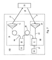
- optical sensor 100 An embodiment of an optical sensor 100 according to the invention will be described with reference to FIG Fig. 7 explained.
- Light emitted by the transmitting unit 13 is split by the coupling 10 onto a measuring fiber 84 and a reference fiber 82.
- Light emerging from the measuring fiber 84 is radiated onto an optical system 15 shown schematically here, which directs the light 17 into a monitoring area 18.
- an optical system 15 shown schematically here, which directs the light 17 into a monitoring area 18.
- a transmitting optical system 16 is formed which guides the light 17 from the transmitting unit 13 into the monitoring area 18.
- optical coupling 11 From an object 19 in the monitoring area 18, light 21 is reflected back and / or backscattered and then passes to an optics 24 shown here schematically.
- the light 21 is subsequently coupled into a glass fiber 23, which is connected to a further optical coupling 11.
- An output of this optical coupling 11 is connected via a further optical fiber 27 to a receiving unit 25 formed by a photodetector.
- another terminal of the optical fiber 24 is connected to the optical coupling 11.
- the optical system 24, the optical fibers 23, 27 and the optical coupling 11 accordingly form a receiving optical unit 22 which directs the light 21 coming from the monitoring area 18 onto the receiving unit 25.
- the optical coupling 11 accordingly serves to conduct both reference pulses via the optical fiber 24 to the receiving unit 25 as well as measurement pulses via the optical fiber 23 to the receiving unit 25.
- pulses supplied by the transmitting unit 13 can be divided into measuring pulses and reference pulses with the aid of the optical coupling 10, which differ substantially only in their height, but not in their shape, due to the particularly effective mixture of modes in the optical coupling 10.
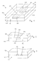
- a first embodiment of an optical coupling 10, as used in an optical sensor according to the invention is, with reference to the FIGS. 1 to 4 explained. Equivalent components are given the same reference numerals in all figures.
- the optical coupling 10 has, as an essential component, a coupling body 20 of a first half-shell 40 and a second half-shell 50.
- the first half shell 40 and the second half shell 50 are each made of a PMMA base material, ie a transparent thermoplastic material.
- An inside or form side 42 of the first half-shell has a recess profile 44, which was thermally impressed there by means of the method described above and a suitable embossing tool.
- a mirror-image-like depression profile 54 is thermally impressed.
- a Lichtleit Geneva is defined.
- the resulting cavities are at least partially, but preferably completely, filled with a lower refractive plastic.
- the first half-shell 40 and the second half-shell 50 are then assembled.
- any optical fiber fibers to be connected may already be inserted into receiving areas provided by the depression profiles 44, 54. In principle, however, this can also take place only after the half shells 40, 50 have been put together.
- a connection region 60 for example for a laser diode 90, is provided. That in the FIGS. 1 and 4 embodiment shown has a Lichtleit Scheme 30 with a branch 36 on. From a portion 38 of the Lichtleit Schemes 30, in which radiation of a laser diode 90 is coupled, accordingly divides the Lichtleit Scheme 30 at the junction 36 in the light guides 32, 34.
- the light-guiding region 30 tapers from the coupling end to the coupling-out end in the in Fig. 4 shown, ie the extension of the light guides 32, 34 in the z-direction is smaller than that of the area 38.
- the Lichtleit Scheme 30 but also tapers in the y-direction, ie in the direction perpendicular to the plane.
- the room seals are in Fig. 4 indicated by a coordinate system 95.
- the region 38 of the Lichtleit Scheme 30 has a substantially rectangular cross-section. This is especially true of the Figures 1 and 2 seen.
- the receiving areas 62, 64 for the optical fibers 82, 84 to be introduced or inserted there have a substantially square cross-section, the receptacle 64, which can receive a measuring fiber 84 of an electro-optical distance measuring device according to the invention, having a larger cross section as the receptacle 62, which serves to receive a reference fiber 82.
- the side lengths of the rectangular entrance surface and the square exit surfaces are on the order of a few 0.1 mm.
- the receptacles 62, 64 are essentially trench-shaped structures or depressions in which the fibers, that is to say the reference fiber 82 and the measuring fiber 84, can be positioned without adjustment.
- FIGS. 1 to 4 illustrated embodiment thus serves as an optical beam splitter for an electro-optical distance measuring device according to the transit time principle.
- FIGS. 5 and 6 A second variant of an optical coupling 10 is in the FIGS. 5 and 6 shown.
- Fig. 5 is a view of the coupling end 12 of the optical coupling 10th
- Fig. 6 shows the Auskoppelende 14 of this optical coupling 10th
- the course of the light guide regions corresponds in the embodiment of the FIGS. 5 and 6 essentially the in Fig. 4 for the first embodiment shown situation.
- the spatial dimensions of the cross sections are again a few 0.1 mm.
- the optical couplings 10 shown in the figures for example, about 50% of an irradiated laser radiation can be coupled into the main channel, that is to say into the measuring fiber 84. For example, only a few percent are injected into the reference fiber 82.
- the branch 36 is made relatively sharp. A rounding leads to a deterioration of the reference decoupling.
- the measuring fiber 84 and the reference fiber 82 are stuck, for example, two millimeters deep in the coupling body 20th
- the present invention provides a novel optical sensor with an optical coupling.
- the optical couplings described here are particularly suitable for applications in optical sensors in general and in particular for those applications in which a targeted beam shaping is necessary. Particular advantages can be achieved here with very small structures, if previously known tool technologies, such as injection molding, do not lead to success.
- these can optical couplings are used according to the invention for electro-optical distance measuring devices according to the transit time principle, in which for the provision of comparable optical pulses, a mode mixture is to take place. Therefore, the optical coupling according to the invention can serve in particular as an optical beam splitter or splitter.
- Compared to previously known technologies such as optical printed circuit boards or simple butt coupling of two fibers side by side can be achieved with the invention significantly improved coupling efficiencies, significantly improved mixing of the individual modes and also a significantly improved reliability of production.
- the good coupling-out efficiency of the reference channel after mode mixing is also significant. Compared to the technology of optical circuit boards also higher numerical apertures can be achieved during coupling and decoupling.
- the hot embossing technology allows overall three-dimensional beam paths within the coupling body and high numerical apertures can be achieved by a large freedom of choice of the material pairings.
- the general objective in the mentioned distance measuring devices according to the transit time principle to couple the highest possible proportion of the light into a measuring fiber and a small defined part in a, in particular shorter, reference fiber, is thus implemented particularly reliably in the optical coupling.
- the same step index fiber can be used, for example, 100 microns in diameter.
- a plastic part can be provided by the optical couplings described here, in which both fibers can be coupled easily and in particular without adjustment.
- the laser diode is also connected without active adjustment with the optical coupling. Since mechanical tolerances of laser diodes are generally comparatively large, it is equally possible to provide suitable adjustment means for the active adjustment of a laser diode.
- the optical couplings described here can basically be operated in a wide temperature range, for example, from -20 to + 75 ° C.
Landscapes
- Physics & Mathematics (AREA)
- Engineering & Computer Science (AREA)
- General Physics & Mathematics (AREA)
- Optics & Photonics (AREA)
- Electromagnetism (AREA)
- Computer Networks & Wireless Communication (AREA)
- Radar, Positioning & Navigation (AREA)
- Remote Sensing (AREA)
- Microelectronics & Electronic Packaging (AREA)
- Health & Medical Sciences (AREA)
- Manufacturing & Machinery (AREA)
- Ophthalmology & Optometry (AREA)
- Mechanical Engineering (AREA)
- Geophysics And Detection Of Objects (AREA)
- Burglar Alarm Systems (AREA)
- Optical Radar Systems And Details Thereof (AREA)
Priority Applications (1)
| Application Number | Priority Date | Filing Date | Title |
|---|---|---|---|
| EP08007360A EP2116867A3 (fr) | 2008-04-15 | 2008-04-15 | Capteur optique |
Applications Claiming Priority (1)
| Application Number | Priority Date | Filing Date | Title |
|---|---|---|---|
| EP08007360A EP2116867A3 (fr) | 2008-04-15 | 2008-04-15 | Capteur optique |
Publications (2)
| Publication Number | Publication Date |
|---|---|
| EP2116867A2 true EP2116867A2 (fr) | 2009-11-11 |
| EP2116867A3 EP2116867A3 (fr) | 2010-03-03 |
Family
ID=41050963
Family Applications (1)
| Application Number | Title | Priority Date | Filing Date |
|---|---|---|---|
| EP08007360A Withdrawn EP2116867A3 (fr) | 2008-04-15 | 2008-04-15 | Capteur optique |
Country Status (1)
| Country | Link |
|---|---|
| EP (1) | EP2116867A3 (fr) |
Cited By (1)
| Publication number | Priority date | Publication date | Assignee | Title |
|---|---|---|---|---|
| DE102010010097A1 (de) * | 2010-03-01 | 2011-09-01 | Esw Gmbh | Kompakter Laser-Entfernungsmesser |
Family Cites Families (11)
| Publication number | Priority date | Publication date | Assignee | Title |
|---|---|---|---|---|
| JPS58149008A (ja) * | 1982-02-28 | 1983-09-05 | Matsushita Electric Works Ltd | 導光路板の製法 |
| GB2141891B (en) * | 1983-05-19 | 1986-09-10 | Barr & Stroud Ltd | Optical range simulator devices |
| JPS59232312A (ja) * | 1983-06-16 | 1984-12-27 | Nippon Telegr & Teleph Corp <Ntt> | 高分子導光路素子およびその製作方法 |
| JPH0312612A (ja) * | 1989-06-09 | 1991-01-21 | Fujitsu Ltd | 光素子間の接続素子 |
| DE4212208A1 (de) * | 1992-04-10 | 1993-10-14 | Bosch Gmbh Robert | Verfahren zur Herstellung optischer Polymerbauelemente mit integrierter Faser-Chip-Kopplung in Abformtechnik |
| US5265177A (en) * | 1992-05-08 | 1993-11-23 | At&T Bell Laboratories | Integrated optical package for coupling optical fibers to devices with asymmetric light beams |
| KR100243315B1 (ko) * | 1996-11-18 | 2000-02-01 | 윤종용 | 다중모드 광커플러 |
| US7298936B1 (en) * | 2000-12-04 | 2007-11-20 | Graywire Llc | Facile production of optical communication assemblies and components |
| JP3607211B2 (ja) * | 2001-03-13 | 2005-01-05 | 株式会社東芝 | 光導波路、光モジュール、光ファイバレーザ装置 |
| AT411402B (de) * | 2001-11-14 | 2003-12-29 | Riegl Laser Measurement Sys | Verfahren zur entfernungsmessung mit einem opto-elektronischen entfernungsmesser |
| JP4694304B2 (ja) * | 2005-08-15 | 2011-06-08 | 株式会社トプコン | 測量装置 |
-
2008
- 2008-04-15 EP EP08007360A patent/EP2116867A3/fr not_active Withdrawn
Cited By (2)
| Publication number | Priority date | Publication date | Assignee | Title |
|---|---|---|---|---|
| DE102010010097A1 (de) * | 2010-03-01 | 2011-09-01 | Esw Gmbh | Kompakter Laser-Entfernungsmesser |
| US8842260B2 (en) | 2010-03-01 | 2014-09-23 | Esw Gmbh | Compact laser rangefinder |
Also Published As
| Publication number | Publication date |
|---|---|
| EP2116867A3 (fr) | 2010-03-03 |
Similar Documents
| Publication | Publication Date | Title |
|---|---|---|
| EP0238977B1 (fr) | Module émission-réception pour un réseau de communication bidirectionnelle, particulièrement un RNIS à large bande | |
| DE19932430C2 (de) | Opto-elektronische Baugruppe sowie Bauteil für diese Baugruppe | |
| DE19610881B4 (de) | Mikrosystembaustein | |
| EP1387982B1 (fr) | Element optique a reflexion totale | |
| DE202005018197U1 (de) | Laser-Entfernungsmessungsvorrichtung | |
| DE102007044010A1 (de) | Zündeinrichtung insbesondere für eine Brennkraftmaschine und Herstellungsverfahren hierfür | |
| DE102008015131B4 (de) | Kraftfahrzeugbeleuchtungseinrichtung und Lichtleiterstruktur für eine Kraftfahrzeugbeleuchtungseinrichtung | |
| DE4113720C2 (de) | Gabellichtschranke | |
| WO2002052321A2 (fr) | Dispositif de transmission de signaux optiques a l'aide de guides d'ondes plans | |
| DE202019103527U1 (de) | Optische Messvorrichtung mit konfokal-chromatischem, optischem Sensor | |
| EP2116867A2 (fr) | Capteur optique | |
| DE102008018740A1 (de) | Elektrooptisches Entfernungsmessgerät, optische Leiterplatte zum Leiten von optischen Signalen und optische Kopplungsvorrichtung | |
| DE102008018927A1 (de) | Optischer Sensor | |
| EP4492104A1 (fr) | Connecteur pour guide d'ondes optique multiple et connecteur pour guide d'ondes optique utilisant un tel connecteur | |
| DE102017204546A1 (de) | Lidarsystem | |
| EP3324218B1 (fr) | Cellule de détection à multifaisceau | |
| EP1760509A2 (fr) | Procédé destiné à l'alignement d'un élément illustré et appareil de mesure aligné selon un tel procédé | |
| DE60027350T2 (de) | Laser-Mikroperforation von thermoplastischen oder cellulosischen Filmen mittels optischer Fasern | |
| DE102009013821B4 (de) | Optischer Sammler und Einrichtung mit optischem Sammler | |
| DE102017209645B4 (de) | Mikromechanische Lichtumlenkvorrichtung, Verfahren zur Umlenkung von Licht mittels einer mikromechanischen Lichtumlenkvorrichtung und Lichtsendevorrichtung | |
| DE2929186C2 (fr) | ||
| DE10120937C2 (de) | Optosensor | |
| DE102014015328B3 (de) | Projektionseinrichtung und Messvorrichtung mit einer solchen | |
| DE102009001471A1 (de) | Lichtquelle | |
| DE102018113970B4 (de) | Kabel mit lichtemittierendem Element |
Legal Events
| Date | Code | Title | Description |
|---|---|---|---|
| PUAI | Public reference made under article 153(3) epc to a published international application that has entered the european phase |
Free format text: ORIGINAL CODE: 0009012 |
|
| AK | Designated contracting states |
Kind code of ref document: A2 Designated state(s): AT BE BG CH CY CZ DE DK EE ES FI FR GB GR HR HU IE IS IT LI LT LU LV MC MT NL NO PL PT RO SE SI SK TR |
|
| AX | Request for extension of the european patent |
Extension state: AL BA MK RS |
|
| PUAL | Search report despatched |
Free format text: ORIGINAL CODE: 0009013 |
|
| AK | Designated contracting states |
Kind code of ref document: A3 Designated state(s): AT BE BG CH CY CZ DE DK EE ES FI FR GB GR HR HU IE IS IT LI LT LU LV MC MT NL NO PL PT RO SE SI SK TR |
|
| AX | Request for extension of the european patent |
Extension state: AL BA MK RS |
|
| AKY | No designation fees paid | ||
| STAA | Information on the status of an ep patent application or granted ep patent |
Free format text: STATUS: THE APPLICATION IS DEEMED TO BE WITHDRAWN |
|
| 18D | Application deemed to be withdrawn |
Effective date: 20100904 |
|
| REG | Reference to a national code |
Ref country code: DE Ref legal event code: R108 Effective date: 20110208 Ref country code: DE Ref legal event code: 8566 |