EP2117116A2 - Verzögerungsdetektionsschaltung, Verzerrungsausgleichsschaltung und Kommunikationsvorrichtung - Google Patents
Verzögerungsdetektionsschaltung, Verzerrungsausgleichsschaltung und Kommunikationsvorrichtung Download PDFInfo
- Publication number
- EP2117116A2 EP2117116A2 EP09152026A EP09152026A EP2117116A2 EP 2117116 A2 EP2117116 A2 EP 2117116A2 EP 09152026 A EP09152026 A EP 09152026A EP 09152026 A EP09152026 A EP 09152026A EP 2117116 A2 EP2117116 A2 EP 2117116A2
- Authority
- EP
- European Patent Office
- Prior art keywords
- signal
- circuit
- delay
- domain
- transmission
- Prior art date
- Legal status (The legal status is an assumption and is not a legal conclusion. Google has not performed a legal analysis and makes no representation as to the accuracy of the status listed.)
- Withdrawn
Links
Images


Classifications
-
- H—ELECTRICITY
- H03—ELECTRONIC CIRCUITRY
- H03F—AMPLIFIERS
- H03F1/00—Details of amplifiers with only discharge tubes, only semiconductor devices or only unspecified devices as amplifying elements
- H03F1/32—Modifications of amplifiers to reduce non-linear distortion
- H03F1/3241—Modifications of amplifiers to reduce non-linear distortion using predistortion circuits
- H03F1/3258—Modifications of amplifiers to reduce non-linear distortion using predistortion circuits based on polynomial terms
-
- H—ELECTRICITY
- H03—ELECTRONIC CIRCUITRY
- H03F—AMPLIFIERS
- H03F3/00—Amplifiers with only discharge tubes or only semiconductor devices as amplifying elements
- H03F3/189—High-frequency amplifiers, e.g. radio frequency amplifiers
-
- H—ELECTRICITY
- H03—ELECTRONIC CIRCUITRY
- H03F—AMPLIFIERS
- H03F2201/00—Indexing scheme relating to details of amplifiers with only discharge tubes, only semiconductor devices or only unspecified devices as amplifying elements covered by H03F1/00
- H03F2201/32—Indexing scheme relating to modifications of amplifiers to reduce non-linear distortion
- H03F2201/3233—Adaptive predistortion using lookup table, e.g. memory, RAM, ROM, LUT, to generate the predistortion
Definitions
- the present invention relates to a delay detection circuit, distortion compensation circuit, and communication apparatus.
- the distortion compensation circuit is circuit which compensates for the distortion in RF signals output from an output amplifier of a communication apparatus;
- the digital predistortion method is a method in which, by further multiplying the distortion of the RF signals by distortion, the distortion is compensated.
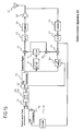
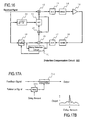
- Fig. 16 is an example of the configuration of a distortion compensation circuit 50 using the digital predistortion method (see for example Japanese Patent Publication No. 4014343 ).
- the LUT (lookup table) 11 stores coefficients (distortion compensation coefficients) which provide the inverse characteristic to the distortion characteristic; the complex multiplier 12 multiplies the baseband signal with coefficients from the LUT 11.
- the baseband signal multiplied by coefficients passes through a D/A converter 13 and quadrature modulator (QDEM) 14 and is output to an amplifier 15.
- the amplifier 15 amplifies and outputs the distortion-compensated (linearity-compensated) RF signal. And, the signal is transmitted from an antenna in a later stage of the amplifier 15 to the communication destination apparatus (other party).
- the distortion compensation circuit 50 updates the coefficients stored in the LUT 11. That is, a subtractor 19 detects the error between the baseband signal and a feedback signal from the amplifier 15, and an adder 21 adds the error to the coefficients of the LUT 11. Then, the coefficients stored in the LUT 11 are updated, on the basis of the added value (sum) and the amplitude of the baseband signal computed by an amplitude calculation portion 20, and thereby the distortion of the RF signal from the amplifier 15 becomes smaller.
- the subtractor 19 compares the baseband signal (reference signal) and the feedback signal from the amplifier 15. Because the feedback signal passes through the D/A converter 13 and quadrature modulator 14 and undergoes signal processing, the quadrature demodulator 16 and A/D converter 17 perform signal processing of the output signal from the amplifier 15.
- the distortion compensation circuit 50 detects the delay amount of the reference signal and feedback signal, by means of the delay detection circuit 51, and based on the delay amount, causes the delay circuit 18 to delay the reference signal.
- the subtractor 19 detects the difference between the reference signal and the feedback signal in a state in which the timing of both coincides.
- Fig. 17A is an example of the configuration of a delay detection circuit 51 of the prior art
- Fig. 17B is an example of delay detection in the prior art (for example, in Japanese Patent Publication No. 4014343 ).
- the delay detection circuit 51 has a delay circuit 510 and correlator 511; the delay circuit 510 delays the reference signal (baseband signal) by a prescribed delay amount, and the correlator 511 outputs the correlation value with the feedback signal.
- the delay amount of the delay circuit 510 is variable; the delay amount (a) for which the output is the maximum becomes the delay amount of the reference signal and feedback signal (see Fig. 17B ).
- the dedicated delay detection circuit 51 must be provided in order to detect the delay amount of the reference signal and feedback signal. For this reason, the circuit scale of the distortion compensation circuit 50 is increased.
- One aspect of the present invention is a delay detection circuit including: a conversion circuit which converts a time-domain signal into a frequency-domain signal or which converts a frequency-domain signal into a time-domain signal, wherein the conversion circuit is used in a signal processing circuit which performs signal processing by quadrature modulation for a transmission signal, and the conversion circuit outputs a delay amount of a first signal with respect to the transmission signal.
- a distortion compensation circuit for compensating distortion in a transmission signal by using distortion compensation coefficient, including: a conversion circuit which converts a time-domain signal into a frequency-domain signal or which converts a frequency-domain signal into a time-domain signal; and a delay circuit which delays the transmission signal or a feedback signal, based on an output of the conversion circuit, wherein the conversion circuit is used in a signal processing circuit which performs signal processing by quadrature modulation for transmission signal; the conversion circuit outputs a delay amount of the feedback signal, with respect to the transmission signal, fed back from output side of the signal processing circuit, or an amount determined from the delay amount; and the distortion compensation coefficient is updated, based on the transmission signal delayed on a basis of the delay amount, or based on the feedback signal delayed on a basis of the amount determined from the delay amount.
- Another aspect of the present invention is a communication apparatus including a signal processing circuit which performs quadrature modulation for a transmission signal and transmits the quadrature modulated transmission signal, including: a conversion circuit which converts a time-domain signal into a frequency-domain signal or which converts a frequency-domain signal into a time-domain signal, wherein the conversion circuit is used in the signal processing circuit; and the conversion circuit outputs a delay amount of a first signal with respect to the transmission signal.
- Fig. 1A is an example of the configuration of a distortion compensation circuit 10.
- the distortion compensation circuit 10 includes a LUT 11, complex multiplier 12, D/A converter 13, quadrature modulator (QMOD) 14, amplifier 15, quadrature demodulator (QDEM) 16, A/D converter 17, delay circuit 18, subtractor 19, amplitude calculator ( ⁇ I 2 +Q 2 ) 20, adder 21, and FFT (Fast Fourier Transform) circuit 22.
- the LUT 11 stores coefficients (distortion compensation coefficients) which are the inverse characteristic of the distortion characteristic of the RF signal, in order to compensate for distortion of the RF signal output from the amplifier 15.
- the complex multiplier 12 performs complex multiplication of baseband signals and coefficients from the LUT 11, and outputs the multiplied baseband signal.
- the D/A converter 13 converts the baseband signal from the complex multiplier 12 into an analog signal.
- the quadrature modulator 14 modulates the baseband signal from the D/A converter 13 and outputs the result as an RF signal.
- the quadrature modulator 14 performs, for example, QPSK (Quaternary Phase Shift Keying), 16QAM (Quadrature Amplitude Modulation), 64QAM, or other quadrature modulation.
- the amplifier 15 amplifies the RF signal from the quadrature modulator 14.
- the quadrature demodulator 16 demodulates the RF signal from the amplifier 15 and outputs a baseband signal.
- the demodulation performed in the quadrature demodulator 16 corresponds to the modulation of the quadrature modulator 14.
- the A/D modulator 17 converts the baseband signal from the quadrature demodulator 16 into a digital signal, and outputs the result to the subtractor 19.
- the delay circuit 18 delays the baseband signal based on the output signal (delay amount) from the FFT circuit 22, and outputs the delayed signal to the subtractor 19.
- the subtractor 19 subtracts the baseband signal (the feedback signal) from the A/D converter 17 and the baseband signal (the reference signal) from the delay circuit 18 to detect the difference (the error) between the two, and outputs an error value.
- the amplitude calculation portion 20 calculates the amplitude of the baseband signal and outputs it to the LUT 11.
- the adder 21 adds the error value from the subtractor 19 and the coefficient output from the LUT 11, and outputs the result to the LUT 11.
- the LUT 11 updates the coefficient based on the amplitude value from the amplitude calculation portion 20 and the addition value from the adder 21.
- the LUT 11 updates coefficients such that the distortion in the RF signal from the amplifier 15 becomes small.
- the FFT circuit 22 inputs the feedback signal from the A/D converter 17, converts the feedback signal, which is a time-domain signal, into a frequency-domain signal, and outputs the result to the delay circuit 18.
- the delay circuit 18 delays the feedback signal based on the output from the FFT circuit 22.
- the distortion compensation circuit 10 can also use a FFT which is used in signal processing circuit to demodulate received signal subjected to OFDM (Orthogonal Frequency Division Multiplexing), OFDMA (Orthogonal Frequency Division Multiplexing Access), and other quadrature modulation, as a delay detection circuit within the distortion compensation circuit 10.
- OFDM Orthogonal Frequency Division Multiplexing
- OFDMA Orthogonal Frequency Division Multiplexing Access
- Fig. 2 is an example of the configuration of a signal processing circuit using OFDM.
- the signal processing circuit includes an IFFT circuit 23, D/A converter 13, quadrature modulator 14, amplifier 15, antenna 24, quadrature demodulator 16, A/D converter 17, and FFT circuit 22.
- Transmission signal for each subcarrier is converted from the frequency domain to time-domain signal by the IFFT 23, the converted signal is modulated by the quadrature modulator 14 after conversion into analog signals by the D/A converter 13, and the modulated signal is transmitted from the antenna 24 after amplification by the amplifier 15.
- a received signal received by the antenna 24 is demodulated by the quadrature demodulator 16 after amplification by the amplifier 25, and the demodulated signal is converted from time-domain signals into frequency-domain received signals for each subcarrier by the FFT circuit 22 after being converted into digital signals by the A/D converter 17
- the distortion compensation circuit 10 uses the FFT circuit 22 which is used in the reception system of an OFDM signal processing circuit, as the delay detection circuit.
- the FFT circuit 22 can be realized using the same circuit as the IFFT circuit 23. This is because in both cases, when the input signal is a frequency-domain signal, the output is a time-domain signal, and when the input is a time-domain signal, the output is a frequency-domain signal.
- the distortion compensation circuit 10 may use the IFFT circuit 23 as the delay detection circuit, in place of the FFT circuit 22.
- Fig. 3 is an example of the configuration of a communication apparatus 30 including the distortion compensation circuit 10.
- the communication apparatus 30 includes, in addition to the distortion compensation circuit 10 of Fig. 1A , a first and second switching unit 31, 32, P/S conversion unit 33, S/P conversion unit 34, and antenna 24.
- the first switching unit 31 inputs the transmission data and the output from the S/P conversion unit 34, and outputs one of these to the IFFT circuit 23.
- the second switching unit 32 outputs the output of the IFFT circuit 23 to either the P/S conversion unit 33 or to the delay circuit 18.
- the P/S conversion unit 33 converts the output from the IFFT circuit 23 into a serial signal.
- the S/P conversion unit 34 converts the output from the A/D converter 17 into parallel signals.
- transmission data passes through the first switching portion 31, is converted from a frequency-domain signal into a time-domain signal by the IFFT circuit 23, passes through the second switching unit 32 and P/S conversion unit 33, and as the baseband signal, is subjected to quadrature modulation and other signal processing by the complex multiplier 12 and other portions.
- the transmission data is transmitted as an RF signal from the antenna 24.
- the communication apparatus 30 performs delay detection
- the feedback signal output from the A/D converter 17 is converted into the parallel signal by the S/P conversion unit 34, and after passing through the first switching unit 31 is input to the IFFT circuit 23.
- the IFFT circuit 23 as the delay detection circuit, outputs the output, via the second switching unit 32, to the delay circuit 18. Subsequent operation is similar to that in Fig. 1A .
- Fig. 4 is an example of the configuration of the communication apparatus 30, including the reception system as well as a OFDM transmission system.
- the IFFT circuit 23 is realized by the same circuit as the FFT circuit 22, and so can be used as transmission processing, as reception processing, and also as the delay detection circuit of the distortion compensation circuit 10.
- Processing of transmission data and the delay detection processing of the distortion compensation circuit 10 are similar to Fig. 3 .
- Processing of received signal is as follows. Received signal received by the antenna 24 is processed by the quadrature demodulator 16, A/D converter 17, and S/P conversion unit 34, and is output from the first switching unit 31 to the IFFT circuit 23.
- the IFFT circuit 23 converts the time-domain received signals to the frequency domain, and outputs the result to the second switching portion 32.
- the second switching unit 32 performs switching so as to output received data to another processing circuit.
- the distortion compensation circuit 10 is a digital circuit up to the D/A converter 13 and following the A/D converter 17.
- the delay in portions comprised by digital circuitry can be calculated at the circuit design time. If there is no delay in signals (feedback signal) processed by the analog circuit from the D/A converter 13 passing through the amplifier 15 to the A/D converter 17, then the FFT circuit 22 (or IFFT circuit 23) can capture feedback signal with a certain timing.
- Fig. 5 is an example of one symbol's worth of OFDM signal. This is an example of OFDM signal output from the quadrature modulator 14, for example. As explained above, if the feedback signal has no delay, then the FFT circuit 22 can be designed in advance so as to capture feedback signal from immediately after the CP (Cyclic Prefix) portion (X in the figure).
- CP Cyclic Prefix
- Fig. 6A and Fig. 6B are examples of a range of the feedback signal captured by the FFT circuit 22 if a delay is and is not present respectively.
- the FFT circuit 22 can capture the signal from "Y" in Fig. 6B .
- Fig. 7 shows an example of a signal series output from the FFT circuit 22.
- the output of the FFT circuit 22 is as follows. F k ⁇ e - j ⁇ 2 ⁇ ⁇ ⁇ ⁇ ⁇ t ⁇ k / n
- Fig. 8 is an example of the graph of the imaginary term.
- the horizontal axis is the delay amount ⁇ t, and the vertical axis is the value of the imaginary term (sin(2 ⁇ t ⁇ k1/n)).
- the output (expression (1)) of the FFT circuit 22 also contains a real term; the value of the real term similarly changes according to the delay amount ⁇ t. That is, the FFT circuit 22 outputs the value (expression (1)) according to the delay amount ⁇ t.
- the delay circuit 18 If the output (expression (1)) of the FFT circuit 22 is output to the delay circuit 18 as the delay amount, and the delay circuit 18 inverts the sign of the output of the FFT circuit 22 and adds the value to the reference signal, then the delay circuit 18 can output the reference signal of the delay amount of the feedback signal. Hence the subtractor 19 can subtract the reference signal and feedback signal at the same timing.
- the distortion compensation circuit 10 uses either the FFT circuit 22 or the IIFT circuit 23 which is used in the signal processing circuitry, as the delay detection circuit of the distortion compensation circuit 10 as well. Hence compared with a case in which a dedicated delay detection circuit is used, the circuit scale of the distortion compensation circuit 10 can be reduced.
- Fig. 1B is an example of the configuration of the another example.
- a delay circuit 182 is provided between the A/D converter 17 and the subtractor 19.
- the FFT circuit 22 is provided between the A/D converter 17 and the delay circuit 182.
- a delay circuit 181 sets, as a delay on the side of the reference signal (feed-forward side), the maximum value of the delay thought to be possible on the feedback side (for example, 100 nsec).
- the FFT circuit 22 detects the delay of the feedback signal (for example, 30 nsec), and sets the difference (for example, 70 nsec; the amount determined from the delay amount) with the maximum value in the delay circuit 182. In this way, the delay circuit 182, to which the output from the FFT circuit 22 is input, may be on the feedback side.
- the delay circuit 18 uses the output from the FFT circuit 22 (or from the IFFT circuit 23) without modification. For example, if the subcarriers used as transmission codes can be ascertained, the subcarriers can also be used to detect delay amounts.
- Fig. 9 is an example of the configuration of the vicinity of the FFT circuit 22.
- a transmission code canceling circuit 35 is provided in the stage following the FFT circuit 22; the output is input to the delay circuit 18.
- the FFT circuit 22 inputs the feedback signal, and outputs the FFT output for the number of subcarriers.
- the transmission code canceling circuit 35 inputs, for example, the transmission code F k1 corresponding to the k1st subcarrier, together with the FFT output, selects the FFT output corresponding to the k1st subcarrier, and divides by the transmission code F k1 .
- the delay circuit 18 delays the reference signal based on the output of the transmission code canceling circuit 35.
- the transmission code F k1 input to the transmission code canceling circuit 35 may for example be transmission data from the stage before the first switching portion 31 which is input to the transmission code canceling circuit 35 in Fig. 3 .
- the transmission code canceling circuit 35 may for example temporarily store the transmission code F k1 , await the output from the FFT circuit 22, select the FFT output corresponding to the k1st subcarrier, and perform division.
- the FFT circuit 22 outputs FFT output for each subcarrier according to the number of subcarriers (expression (1)).
- Embodiment 1 explains an example using one point thereamong. For example, a plurality of points can also be used in delay detection. Such an application example is explained below, focusing on two points.
- the FFT outputs corresponding to the k1st and the k2nd subcarriers can be expressed as follows.
- k2 > k1
- the k2nd (k2-th) subcarrier frequency is higher than that of the k1st (k1-th) subcarrier.
- Fig. 10 is an example of a graph of the imaginary term of each of the outputs of expressions (2) and (3).
- the output corresponding to the k2nd subcarrier has a narrower range of detection of the delay amount ⁇ t than the k1st output.
- a larger output is obtained, even for a small change in the delay amount ⁇ t, from the k2nd than from the k1st subcarrier. That is, the output for a subcarrier of higher frequency has a smaller detection width of the delay amount ⁇ t, but is larger value, even for a small change in the delay amount ⁇ t, than at a lower frequency.
- the resolution (number of bits) of detection of the delay amount ⁇ t can also be adjusted. For example, when the delay amount ⁇ t can be represented using a larger number of bits, the k2nd output, at a higher frequency, can be used to detect the delay, and when the delay amount ⁇ t can be represented using a smaller number of bits, the k1st output at the lower frequency can be used.
- the output from the FFT circuit 22 may be used according to the number of bits that can be used by the delay circuit 18.
- the delay circuit 18 can use the k1st output at the lowest frequency to delay the reference signal (coarse adjustment), and then, when the delay amount ⁇ t is made small, can use the k2nd output at a higher frequency to delay the signal (fine adjustment).
- Embodiment 1 delays were considered in designing the component portions of the digital circuit in advance at circuit design time; for example, design was performed such that the FFT circuit 22 captures the feedback signal with the timing of "X" in Fig. 5 .
- the Embodiment 4 is an example in which delay detection is performed without taking delays into consideration at circuit design time.
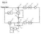
- Fig. 11 is an example of the configuration of the distortion compensation circuit 10 of Embodiment 4.
- the subtractor 25 takes the difference between the reference signal and the feedback signal, and the difference value is input to the FFT circuit 22.
- a delay ⁇ tr occurs in the reference signal
- a delay ⁇ tf occurs in the feedback signal.
- the delay of the feedback signal relative to the reference signal is ( ⁇ tf- ⁇ tr).
- the delay amount ( ⁇ tf- ⁇ tr) is input to the FFT circuit 22, the output is as follows.
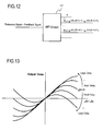
- Fig. 12 is an example of a signal series output from the FFT circuit 22;
- Fig. 13 is a graph showing an example of the output of the imaginary term among the output of expression (4), similarly to Embodiment 1.
- the output from the FFT circuit 22 is input to the delay circuit 18, so that similarly to Embodiment 1, when the output is negative the reference signal delay is increased, but when the output is positive the reference signal delay is decreased.
- subtraction can be performed in a state in which the timing of the reference signal and the feedback signal coincide in the input stage of the subtractor 19.
- Embodiment 5 is an example in which the feedback signal capturing range for the FFT circuit 22 in Embodiment 1 and similar is a short range compared with Embodiment 1.
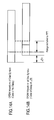
- Fig. 14A and Fig. 14B are examples.
- Fig. 15 is an example of the configuration of Embodiment 5.
- a counter 40 is provided between the A/D converter 17 and the S/P conversion portion 34.
- the counter 40 in which a count value is stored in advance, counts the number of input signal samples in a fixed interval, and outputs the counted input signals. By making the count value within the range shown in Fig. 14B , the capturing range of the FFT circuit 22 can be made short compared with Embodiment 1.
- the distortion compensation circuit, the communication apparatus, and the delay detection circuit, with reduced circuit scale can be provided.
Landscapes
- Physics & Mathematics (AREA)
- Engineering & Computer Science (AREA)
- Power Engineering (AREA)
- Algebra (AREA)
- General Physics & Mathematics (AREA)
- Mathematical Analysis (AREA)
- Mathematical Optimization (AREA)
- Pure & Applied Mathematics (AREA)
- Nonlinear Science (AREA)
- Transmitters (AREA)
- Amplifiers (AREA)
Applications Claiming Priority (1)
| Application Number | Priority Date | Filing Date | Title |
|---|---|---|---|
| JP2008121455A JP2009272875A (ja) | 2008-05-07 | 2008-05-07 | 遅延検出回路、歪み補償回路、及び通信装置 |
Publications (1)
| Publication Number | Publication Date |
|---|---|
| EP2117116A2 true EP2117116A2 (de) | 2009-11-11 |
Family
ID=40863400
Family Applications (1)
| Application Number | Title | Priority Date | Filing Date |
|---|---|---|---|
| EP09152026A Withdrawn EP2117116A2 (de) | 2008-05-07 | 2009-02-04 | Verzögerungsdetektionsschaltung, Verzerrungsausgleichsschaltung und Kommunikationsvorrichtung |
Country Status (3)
| Country | Link |
|---|---|
| US (1) | US20090279641A1 (de) |
| EP (1) | EP2117116A2 (de) |
| JP (1) | JP2009272875A (de) |
Families Citing this family (3)
| Publication number | Priority date | Publication date | Assignee | Title |
|---|---|---|---|---|
| WO2011030672A1 (ja) * | 2009-09-10 | 2011-03-17 | 日本電気株式会社 | サンプリング回路、通信装置、歪補償回路、信号サンプリング方法、プログラム |
| JP6547621B2 (ja) * | 2015-12-25 | 2019-07-24 | アイコム株式会社 | 送信機および歪補正方法 |
| US10666303B1 (en) * | 2018-04-13 | 2020-05-26 | Nxp Usa, Inc. | Spurious signal cancellation in radio frequency transmitters |
Citations (1)
| Publication number | Priority date | Publication date | Assignee | Title |
|---|---|---|---|---|
| JPH0414343B2 (de) | 1983-05-07 | 1992-03-12 | Konishiroku Photo Ind |
Family Cites Families (5)
| Publication number | Priority date | Publication date | Assignee | Title |
|---|---|---|---|---|
| FR2707127A1 (fr) * | 1993-06-29 | 1995-01-06 | Philips Laboratoire Electroniq | Système de transmission numérique à prédisposition. |
| JP4014343B2 (ja) * | 1999-12-28 | 2007-11-28 | 富士通株式会社 | 歪補償装置 |
| KR100532422B1 (ko) * | 2003-02-28 | 2005-11-30 | 삼성전자주식회사 | 동일 심볼을 다수의 채널에 중복적으로 전송하여 통신거리를 확장시킨 무선 랜 시스템의 직교 주파수 분할다중화 송수신 장치 및 그 송수신 방법 |
| JP4255361B2 (ja) * | 2003-11-07 | 2009-04-15 | 富士通株式会社 | 歪み補償増幅器 |
| JP5034319B2 (ja) * | 2006-05-26 | 2012-09-26 | 富士通株式会社 | 歪補償装置及び歪補償方法 |
-
2008
- 2008-05-07 JP JP2008121455A patent/JP2009272875A/ja not_active Withdrawn
-
2009
- 2009-01-29 US US12/362,235 patent/US20090279641A1/en not_active Abandoned
- 2009-02-04 EP EP09152026A patent/EP2117116A2/de not_active Withdrawn
Patent Citations (1)
| Publication number | Priority date | Publication date | Assignee | Title |
|---|---|---|---|---|
| JPH0414343B2 (de) | 1983-05-07 | 1992-03-12 | Konishiroku Photo Ind |
Also Published As
| Publication number | Publication date |
|---|---|
| US20090279641A1 (en) | 2009-11-12 |
| JP2009272875A (ja) | 2009-11-19 |
Similar Documents
| Publication | Publication Date | Title |
|---|---|---|
| US7606322B2 (en) | Digital pre-distortion technique using nonlinear filters | |
| EP1037442B1 (de) | OFDM Kommunikationssystem | |
| CN101656512B (zh) | 功率放大器非线性程度度量装置、方法和预失真补偿装置 | |
| EP1418720B1 (de) | Empfänger in einem OFDM-Übertragungssystem | |
| KR100555508B1 (ko) | 직교 주파수 분할 다중 수신 시스템에서의 임펄스 잡음억제 회로 및 방법 | |
| US9225296B2 (en) | Method and system for aligning signals widely spaced in frequency for wideband digital predistortion in wireless communication systems | |
| KR101127467B1 (ko) | Iq 부정합을 추정 및 보상하는 수신기 | |
| KR101120685B1 (ko) | 피크 억압 방법 | |
| US8588711B2 (en) | Transmission apparatus and distortion compensation method | |
| EP1596551B1 (de) | Vorrichtung zur Verringerung des Verhältnisses von Spitzen- zu Durchschnittsleistung in einem Mehrträgersystem | |
| US8442157B2 (en) | Wireless apparatus and signal processing method | |
| US8000661B2 (en) | Communication system with frequency-adaptive predistorter design | |
| WO2001020831A1 (en) | Ofdm communication device and detecting method | |
| JP2006148854A (ja) | マルチキャリア受信機及び遅延補正機能付き送信機 | |
| US7769358B2 (en) | Radio system, radio transmitter, and radio receiver | |
| JP2004080731A (ja) | Ofdm受信装置及びofdm信号の補正方法 | |
| JP5147089B2 (ja) | Ofdm通信システムにおけるアナログ損失のハイブリッドドメイン補償パラメータの求め方と補償方法 | |
| CN101471688A (zh) | 取样频率偏移估计与补偿装置与方法 | |
| US20060256885A1 (en) | Apparatus and method for estimating carrier-to-interference-and-noise ratio in an orthogonal frequency division multiplexing system | |
| EP2765746B1 (de) | Verfahren und vorrichtung zur verarbeitung von daten | |
| EP2117116A2 (de) | Verzögerungsdetektionsschaltung, Verzerrungsausgleichsschaltung und Kommunikationsvorrichtung | |
| EP1819040A1 (de) | Verzerrungsausgleichvorrichtung und Verfahren | |
| KR100431008B1 (ko) | 극좌표계를 이용하여 구현한 오에프디엠 수신장치 및 방법 | |
| WO2009011071A1 (en) | Amplifier device with nonlinear-distortion compensation | |
| JP2008017218A (ja) | 無線通信装置 |
Legal Events
| Date | Code | Title | Description |
|---|---|---|---|
| PUAI | Public reference made under article 153(3) epc to a published international application that has entered the european phase |
Free format text: ORIGINAL CODE: 0009012 |
|
| AK | Designated contracting states |
Kind code of ref document: A2 Designated state(s): AT BE BG CH CY CZ DE DK EE ES FI FR GB GR HR HU IE IS IT LI LT LU LV MC MK MT NL NO PL PT RO SE SI SK TR |
|
| AX | Request for extension of the european patent |
Extension state: AL BA RS |
|
| STAA | Information on the status of an ep patent application or granted ep patent |
Free format text: STATUS: THE APPLICATION IS DEEMED TO BE WITHDRAWN |
|
| 18D | Application deemed to be withdrawn |
Effective date: 20140902 |