EP2120260B1 - Unité de semi-conducteur avec capteur thermique - Google Patents
Unité de semi-conducteur avec capteur thermique Download PDFInfo
- Publication number
- EP2120260B1 EP2120260B1 EP09004530.3A EP09004530A EP2120260B1 EP 2120260 B1 EP2120260 B1 EP 2120260B1 EP 09004530 A EP09004530 A EP 09004530A EP 2120260 B1 EP2120260 B1 EP 2120260B1
- Authority
- EP
- European Patent Office
- Prior art keywords
- temperature sensor
- semiconductor chip
- ceramic substrate
- semiconductor
- temperature
- Prior art date
- Legal status (The legal status is an assumption and is not a legal conclusion. Google has not performed a legal analysis and makes no representation as to the accuracy of the status listed.)
- Ceased
Links
Images

Classifications
-
- H—ELECTRICITY
- H10—SEMICONDUCTOR DEVICES; ELECTRIC SOLID-STATE DEVICES NOT OTHERWISE PROVIDED FOR
- H10W—GENERIC PACKAGES, INTERCONNECTIONS, CONNECTORS OR OTHER CONSTRUCTIONAL DETAILS OF DEVICES COVERED BY CLASS H10
- H10W40/00—Arrangements for thermal protection or thermal control
Definitions
- the present invention relates to a semiconductor unit that includes a means for detecting a temperature of a semiconductor chip mounted on a circuit pattern of a ceramic substrate.
- a temperature of the semiconductor unit is detected by a temperature detector to prevent damage on a semiconductor chip due to an excessive temperature rise caused by driving the semiconductor chip.
- a semiconductor unit disclosed for example, in Japanese Unexamined Patent Application Publication No. 2002-76236
- the drive of the semiconductor chip is shut down.
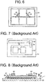
- semiconductor chips 53 are mounted on one of circuit patterns 52 formed on a ceramic substrate 51.
- One of the terminals of a thermistor 54 is soldered to the circuit pattern 52 on which the semiconductor chips 53 are mounted.
- the other terminal of the thermistor 54 is soldered to the different circuit pattern 52.
- a temperature of the semiconductor chip can be directly detected.
- a temperature of semiconductor chips 63 mounted on a ceramic substrate 61 can be detected also by an external thermistor 66.
- the thermistor 66 is mounted on a metal base 65 by a screw 67.
- the ceramic substrate 61 has a circuit pattern 62 formed on the upper surface of a ceramic plate 69.
- Each of the semiconductor chips 63 is mounted on the circuit pattern 62 by solder H.
- the ceramic substrate 61 has a metal plate 68 bonded to the lower surface of the ceramic plate 69 and mounted on the metal base 65 by solder H.
- the thermistor 54 when the thermistor 54 is mounted on the ceramic substrate 51 by soldering, the thermistor 54 need to be located across the different circuit patterns 52, and the process of manufacturing the semiconductor unit becomes complicated, accordingly. In addition, since one of the terminals of the thermistor 54 is soldered to the circuit pattern 52 on which the semiconductor chip 53 is mounted, the thermistor 54 is affected by noise generated by the switching operation of the semiconductor chips 53.
- the temperature sensor is incorporated in the semiconductor chip, the temperature sensor is affected by noise generated due to the switching operation of the semiconductor chip. Therefore, though the temperature sensor is located close to the semiconductor chip, a temperature of the semiconductor chip cannot be detected accurately. Additionally, in semiconductor units having a plurality of identical semiconductor chips, a temperature is generally detected at not all the semiconductor chips, but only at one semiconductor chip and, therefore, a space for connecting the temperature sensor in the other semiconductor chips of which temperature are not detected becomes useless. Furthermore, in the case of parallel-connected semiconductor chips used in an inverter so that a large amount of current flows through each arm, temperatures of all the semiconductor chips in each arm need not to be detected. However, the size of the semiconductor chip incorporating the temperature sensor is large, resulting in enlargement of the entire size of the semiconductor unit.
- the present invention is directed to providing a semiconductor unit that allows more accurate detection of a temperature of a semiconductor chip mounted on a circuit pattern of a ceramic substrate without enlarging the size of the unit.
- DE 196 30 902 A1 discloses a semiconductor unit with semiconductor chips on a ceramic substrate.
- a silicon resistor onto a floating dedicated partial surface of a circuit pattern on the ceramic substrate, and to further connect the silicon resistor via bonding wires.
- IBM Tech. Disc. Bull. 33, no. 4, pp. 442/443 discloses a piston that is pressed via a spring onto a chip.
- the piston there is machined a hole and in this hole there is embedded a thermocouple via thermally conductive epoxy resin.
- DE 195 23 010 A1 discloses an arrangement of a power semiconductor and an ASIC on a common substrate which consists of a metal plate being coated with a ceramic layer. A sheet spring presses the power semiconductor against the substrate.
- the respective teaching considers cases in which a temperature sensor can be integrated into the ASIC together with an evaluation circuitry without any problems, because the cost of the ASIC is only increased insignificantly by the integration of the temperature supervisor. In this way, it is not disclosed a pressing member for retaining a temperature sensor by pressing it against the ceramic substrate.
- DE 36 43 288 A1 discloses a couple of pressing member arrangements.
- a semiconductor unit includes a semiconductor chip, a ceramic substrate having a circuit pattern on which the semiconductor chip is mounted, and a temperature sensor for detecting a temperature.
- the semiconductor unit further includes a pressing member for retaining the temperature sensor by pressing against the ceramic substrate.
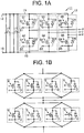
- the inverter 11 (semiconductor unit) has an inverter circuit 12 including six switching devices Q1, Q2, Q3, Q4, Q5 and Q6.
- MOSFET metal-oxide-semiconductor field-effect transistor
- the serially connected pairs of switching devices Q1 and Q2, Q3 and Q4, and Q5 and Q6 are connected in parallel.
- Diodes D1, D2, D3, D4, D5 and D6 are inversely connected in parallel to the switching devices Q1, Q2, Q3, Q4, Q5 and Q6, respectively.
- Each of pairs of the switching device and the diode Q1 and D1, Q3 and D3, and Q5 and D5 is referred to as an upper arm.
- Each of pairs of the switching device and the diode Q2 and D2, Q4 and D4, and Q6 and D6 is referred to as a lower arm.
- each of the switching devices Q1, Q3 and Q5 has a drain terminal connected to a positive input terminal 14 via a line 13, and each of the switching devices Q2, Q4 and Q6 has a source terminal connected to a negative input terminal 16 via a line 15.
- Plural capacitors 17 are connected in parallel between the lines 13 and 15. In the present embodiment, an electrolytic capacitor is used for the capacitors 17.
- Each capacitor 17 has a positive terminal connected to the line 13 and a negative terminal connected to the line 15.
- a node between the switching devices Q1 and Q2 is connected to a U-phase terminal U
- a node between the switching devices Q3 and Q4 is connected to a V-phase terminal V
- a node between the switching devices Q5 and Q6 is connected to a W-phase terminal W.
- Each of the switching devices Q1, Q2, Q3, Q4, Q5 and Q6 has a gate terminal connected to signal terminals G1, G2, G3, G4, G5 and G6, and has a source terminal connected to signal terminals S1, S2, S3, S4, S5 and S6. respectively.
- each of the upper and lower arms is composed of one switching device and one diode, but each arm may be composed of plural pairs of a switching device Q and a diode D connected in parallel, as shown in Fig. 1B .
- each arm is composed of four pairs of the switching device Q and the diode D.
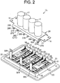
- the inverter 11 includes a metal base 20, ceramic substrates 21 and semiconductor chips 23.
- the metal base 20 is made of copper alloy and cooperates with the ceramic substrates 21 to form a base plate.
- the semiconductor chips 23 are mounted on the ceramic substrates 21.
- Each semiconductor chip 23 has one switching device (MOSFET) and one diode in combination as a one-chip device. That is, each semiconductor chip 23 has one switching device Q and one diode D of Fig. 1B .
- each ceramic substrate 21 has circuit patterns 24A, 24B, 24C and 24D formed on the upper surface of a ceramic plate 26.
- the ceramic substrate 21 has a metal plate (not shown) on the lower surface of the ceramic plate 26, so as to bond to the metal base 20.
- the ceramic plate 26 is made of, for example, aluminum nitride, alumina or silicon nitride.
- the circuit patterns 24A, 24B, 24C and 24D and the metal plate are made of, for example, aluminum or copper.
- the ceramic substrate 21 is soldered to the metal base 20 with the metal plate.
- the metal base 20 is described as the bottom of the inverter 11.
- each of the metal base 20 and the ceramic substrates 21 has a generally rectangular shape.
- a total of twelve ceramic substrates 21 are arranged in six rows and two columns on the metal base 20 so that longitudinal directions of the ceramic substrate 21 and the longitudinal direction of the metal base 20 are perpendicular to each other.
- Each of the upper and lower arms of the inverter circuit 12 (see Fig. 1A ) is composed of the semiconductor chips 23 mounted on two ceramic substrates 21 arranged in each row, and three pairs of the upper and lower arms are arranged on the metal base 20.
- each ceramic substrate 21 has two semiconductor chips 23 and, therefore, each arm is composed of four semiconductor chips 23. It is noted that Fig. 3 shows the second pair of the upper and lower arms.
- the circuit pattern 24A is for conducting a gate signal
- the circuit pattern 24B is for conducting a drain current
- the circuit pattern 24C is for conducting a source current
- the circuit pattern 24D is for conducting a source signal.
- the semiconductor chip 23 is mounted on the circuit pattern 24B by soldering.
- the gate of the semiconductor chip 23 is electrically connected to the circuit pattern 24A by wire bonding
- the source of the semiconductor chip 23 is electrically connected to the circuit patterns 24C and 24D by wire bonding.
- the inverter 11 includes a positive conductor 27 and a negative conductor 28.
- the positive and negative conductors 27 and 28 are made of a conductive plate and arranged above the metal base 20.
- the positive and negative conductors 27 and 28 are disposed adjacent and parallel to each other and respectively extend parallel to the metal base 20.
- the positive and negative conductors 27 and 28 are insulated from each other through an insulator (not shown) interposed therebetween.
- the negative conductor 28 is placed over the positive conductor 27, and four capacitors 17 are arranged on the negative conductor 28 with the positive and negative terminals thereof facing downward.
- the positive and negative conductors 27 and 28 serve as the lines 13 and 15 of Fig. 1A , respectively.
- the positive conductor 27 includes three pairs of terminal portions 27A that extend from both end sides of the positive conductor 27 toward the ceramic substrates 21.
- the terminal portion 27A is then bent so as to extend parallel to the upper surface of the positive conductor 27 to form a terminal end 27B that is joined to the circuit pattern 24B.
- the negative conductor 28 also includes similar terminal portions 28A respectively having a terminal end 28B that is joined to the circuit pattern 24C.
- the positive and negative conductors 27 and 28 further include side portions 27C and 28C from which the terminal portions 27A and 28A extend downward, respectively.
- the side portions 27C and 28C are disposed adjacent to each other.
- the inverter 11 includes a frame 30 made of a non-conductive material.
- the frame 30 is of a rectangular shape and mounted around the ceramic substrates 21 on the metal base 20.
- a positive input terminal 14 is formed at a longitudinal end of the positive conductor 27 so as to extend outward of the frame 30.
- a negative input terminal 16 is formed at a longitudinal end of the negative conductor 28 opposite from the positive input terminal 14 so as to extend outward of the frame 30.
- the inverter 11 includes three output electrodes 32U, 32V and 32W having a generally L shape as viewed in the longitudinal direction of the metal base 20. Horizontal portions of the output electrodes 32U, 32V and 32W extend below the positive conductor 27 in a direction that is perpendicular to longitudinal direction of the positive conductor 27. Vertical portions of the output electrodes 32U, 32V and 32W extend upward at a position near the wall of the frame 30.
- the horizontal portion is formed with four connecting portions 33 that are joined to the circuit patterns 24B and 24C. Two of the four connecting portions 33 are located at the end of the horizontal portion away from the vertical portion, and the rest of the four connecting portions 33 are located at a position near the vertical portion.
- the electrodes 32U, 32V and 32W are insulated from the positive conductor 27 through silicone gel (not shown).
- the output electrode 32U is mounted by ultrasonic bonding on the circuit patterns 24C of the upper arm composed of the switching device Q1 and the diode D1, and on the circuit patterns 24B of the lower arm composed of the switching device Q2 and the diode D2.
- the output electrode 32V is mounted by ultrasonic bonding on the circuit patterns 24C of the upper arm composed of the switching device Q3 and the diode D3, and on the circuit patterns 24B of the lower arm composed of the switching device Q4 and the diode D4.
- the output electrode 32W is mounted by ultrasonic bonding on the circuit patterns 24C of the upper arm composed of the switching device Q5 and the diode D5, and on the circuit patterns 24B of the lower arm composed of the switching device Q6 and the diode D6.
- signal terminals G1, G2, G3, G4, G5 and G6 are connected to the circuit patterns 24A of the ceramic substrates 21 that are located away from the vertical portions of the output electrodes 32U, 32V and 32W.
- Signal terminals S1, S2, S3, S4, S5 and S6 are connected to the circuit patterns 24D of the ceramic substrates 21 that are located away from the vertical portions of the output electrodes 32U, 32V and 32W.
- the signal terminals G1 through G6 and S1 through S6 are molded integrally with the frame 30, and projecting outward of the frame 30.
- Two adjacent circuit patterns 24A of the ceramic substrates 21 of each arm are connected to each other by wire bonding, and two adjacent circuit patterns 24D of the ceramic substrates 21 of each arm are connected to each other by wire bonding.
- the inverter 11 includes a temperature sensor 34 to detect a temperature of the semiconductor chip 23 mounted on the circuit pattern 24B.
- the temperature sensor 34 is mounted by press fitting to a projecting end of a support plate 35 that is fixed to the frame 30 by a screw 36 and projected over the ceramic substrate 21 from the frame 30.
- a leaf spring is used for the support plate 35.
- the temperature sensor 34 is composed of a cylindrical case 37, a signal wire 38 and a thermistor 34A.
- the cylindrical case 37 is made of a metal having a high thermal conductivity such as copper, aluminum or stainless steel.
- the signal wire 38 extends out of the cylindrical case 37.
- the thermistor 34A is received in the cylindrical case 37 and sealed by an electrically insulating material having a high thermal conductivity.
- the temperature sensor 34 detects a temperature of the semiconductor chip 23 with the end of the cylindrical case 37 pressed to the ceramic substrate 21.
- the support plate 35 functions as a pressing member that keeps the temperature sensor 34 pressed to the ceramic substrate 21.
- the temperature sensor 34 is pressed to the circuit pattern 24B on which the semiconductor chips 23 are mounted. If a pressing force that the ceramic substrate 21 receives from the temperature sensor 34 is too large, the ceramic substrate 21 may be damaged. Therefore, it is preferable that a pressing force that the support plate 35 provides to the ceramic substrate 21 is as large as, for example, 50 N or less so as to prevent the damage on the ceramic substrate 21. Specifically, it is preferable that the pressing force is, for example, in the range of 10 to 30 N so as to provide an adequate pressing force to the ceramic substrate 21.
- the inverter 11 is used as, for example, a part of a vehicle power supply.
- the positive and negative input terminals 14 and 16 are connected to a DC power supply (not shown)
- the U-phase terminal U, the V-phase terminal V and the W-phase terminal W are connected to a motor (not shown)
- the signal terminals G1 through G6 and S1 through S6 arc connected to a controller (not shown).
- the signal wire 38 of the temperature sensor 34 is connected to the controller.
- Such switching operation of the switching devices Q1 through Q6 generates a rapid rise or fall of currents flowing through the positive and negative conductors 27 and 28 in opposite directions. Since the positive and negative conductors 27 and 28 both have a plate shape and disposed parallel to and adjacent to each other, the line inductance is lowered because of the mutual inductance. In addition, the side portions 27C and 28C of the positive and negative conductors 27 and 28 are also disposed parallel to and adjacent to each other, and the line inductance is therefore reduced, as compared to a case wherein such parallel side portions are not provided.
- the controller controls the operation of the switching devices Q1 through Q6, that is, the operation of the semiconductor chips 23 so that power is supplied to the load as required.
- the switching operation of the semiconductor chip 23 causes generation of heat in the semiconductor chip 23.
- the heat is transferred to the metal base 20 and then radiated into the atmosphere.
- a temperature of the semiconductor chip 23 may increase above the upper temperature limit.
- the semiconductor chip 23 may be damaged.
- the temperature sensor 34 detects a temperature that corresponds to a temperature of the semiconductor chip 23, and outputs a detection signal to the controller. Based on the detection signal, the controller controls the switching operation of the semiconductor chip 23 so that a temperature around the semiconductor chip 23 does not exceed the upper temperature limit.
- the temperature sensor 34 detects a temperature in the condition of being pressed to the ceramic substrate 21 that has the circuit pattern 24B on which the semiconductor chips 23 are mounted.
- the controller receives the detection signal from the temperature sensor 34, and calculates a temperature of the semiconductor chip 23 based on a map or a function previously stored in a memory. Since heat transfer resistance of a path from the semiconductor chip 23 to the temperature sensor 34 is smaller, as compared to the one in the conventional external sensor of Fig. 8 , the temperature of the semiconductor chips 23 can be detected more accurately.
- the temperature sensor 34 needs only to be pressed to some part of the ceramic substrate 21, a space for the temperature sensor 34 can be easily provided without enlarging the size of the semiconductor unit. Thus, the size of the semiconductor unit can be reduced, as compared to a size wherein a semiconductor chip incorporating a temperature sensor is used.
- the inverter 11 according to the first embodiment has the following advantages.
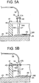
- Fig. 5A shows a pressing member according to a comparative example.
- the pressing member is provided by a coil spring 40.
- the cylindrical case 37 of the temperature sensor 34 is inserted in a through hole 39A of a rigid support plate 39 that is mounted to the frame 30 by a bolt 41.
- the coil spring 40 is disposed between the support plate 39 and a flange portion 37A of the cylindrical case 37.
- the ends of the coil spring 40 are respectively fixed to the support plate 39 and the flange portion 37A.
- the coil spring 40 urges the cylindrical case 37 toward the ceramic substrate 21. That is, the length from a part where the cylindrical case 37 projects below the support plate 39 to the end before the support plate 39 is mounted to the frame 30 is longer than the length after the support plate 39 is mounted to the frame 30.
- the end of the cylindrical case 37 of the temperature sensor 34 is kept pressed to the circuit pattern 24B adequately by a spring force of the coil spring 40.
- Fig. 5B shows a pressing member according to the second embodiment of the present invention.
- the pressing member of the second embodiment is provided by a support plate 42.
- the support plate 42 is made of a resin and mounted to the frame 30 by the bolt 41.
- the support plate 42 is projected over the ceramic substrate 21 from the frame 30.
- the temperature sensor 34 is mounted to the projecting end of the support plate 42 and pressed to the circuit pattern 24B by bending elasticity of the support plate 42. That is, the support plate 42 is a leaf spring made of a resin.
- the cylindrical case 37 of the temperature sensor 34 includes a flange portion 37B, the outer peripheral surface of which is rounded.
- the cylindrical case 37 is inserted in a through hole 42A formed in the support plate 42, and mounted to the support plate 42 via the flange portion 37B.
- the support plate 42 which is in a curved shape before being mounted to the frame 30, is straightened by screwing the bolt 41 into the frame 30.
- the support plate 42 is thus mounted to the frame 30 while extending parallel to the metal base 20, thereby keeping the temperature sensor 34 pressed to the circuit pattern 24B.
- Each of the support plates 35, 39 and 42 may be supported at both ends.
- the support plate 35 when the support plate 35 is mounted to a rectangular frame 43 like a lattice, the support plate 35 is located across the cross bars of the frame 43 so as to be supported at both ends, and the temperature sensor 34 is mounted to the middle of the support plate 35.
- the temperature sensor 34 can be supported more stably, as compared to a case wherein the support plate 35 is supported at one end.
- the temperature sensor 34 needs not to be pressed to the circuit pattern 24B on which the semiconductor chip 23 is mounted.
- the temperature sensor 34 may be pressed to the circuit pattern 24C on which the semiconductor chip 23 is not mounted, or may be pressed directly to the ceramic plate 26.
- the temperature sensor 34 arranged so as to be in contact with the circuit pattern 24B results in more accurate detection of the temperature of the semiconductor chip 23.
- the temperature sensor 34 includes the thermistor 34A received in the cylindrical case 37.
- a diode may be received in the cylindrical case 37. Since the current-voltage characteristic of a diode is highly dependent on a temperature, for example, when a diode is used for the temperature sensor 34, a temperature of the semiconductor chip 23 can be detected based on the variation of the current-voltage characteristic that is previously stored in a memory.
- the cylindrical case 37 constituting the temperature sensor 34 may have a polygon shape or an ellipse shape in the cross section.
- a temperature sensor such as a thermistor or a diode may be received in a box-shaped case.
- An electrically conductive material having a high thermal conductivity may be used for sealing a temperature sensor (thermistor 34A) received in the cylindrical case 37.
- the temperature sensor is affected by an electric potential at the circuit patterns 24B and 24C when the cylindrical case 37 is in contact with the circuit patterns 24B and 24C. Therefore, a temperature of the semiconductor chip 23 needs to be calculated from the detection signal of the temperature sensor, with consideration of the effect of the electric potential.
- the support plates 35, 39 and 42 need not to be a rectangular plate.
- the support plates 35, 39 and 42 may be in the form of a crank or may have an L shape when being.
- the support plates 35, 39 and 42 may have a generally U shape
- the inverter 11 may include plural temperature sensors 34.
- each of the upper and lower arms may include one temperature sensor 34, or each of the pairs of the upper and lower arms may include one temperature sensor 34.
- each arm may be less than or more than four, depending on the amount of current flowing through each arm.
- each arm may be composed of one switching device Q and one diode D.
- a pair of one switching device and one diode is incorporated in the semiconductor chip 23 as a package.
- the switching device and the diode may be separately mounted on the different circuit patterns.
- the inverter 11 may be composed of two pairs of the upper and lower arms for generating single-phase AC.
- the present invention may be applied not only to an inverter but also to a DC-DC converter.
- the number of the capacitors 17 may be less than or more than four, depending on the rated current of the inverter 11 and the capacitance of the capacitor 17. Alternatively, the inverter 11 may include no capacitor 17.
- Power transistors such as an insulated-gate bipolar transistor (IGBT) or a thyristor may be used for the semiconductor chip 23.
- IGBT insulated-gate bipolar transistor
- thyristor a thyristor
Landscapes
- Inverter Devices (AREA)
- Cooling Or The Like Of Semiconductors Or Solid State Devices (AREA)
- Measuring Fluid Pressure (AREA)
Claims (7)
- Unité à semi-conducteur (11), comprenant :une puce à semi-conducteur (23) ;une base métallique (20) ;un châssis (30) réalisé en un matériau non conducteur;un substrat de céramique (21) monté sur la base métallique (20), le substrat de céramique (21) présentant une configuration de circuit (24B) sur laquelle la puce à semi-conducteur (23) est montée ; etun capteur de température (34) pour détecter une température,dans laquellel'unité à semi-conducteur (11) comprend en outre un élément de pression (35, 40, 42) pour retenir le capteur de température (34) par pression contre le substrat de céramique (21),dans laquelle le capteur de température (34) est monté par ajustement serré sur une extrémité saillante d'une plaque de support (35) qui est fixée au châssis (30), et la plaque de support (35) est un ressort à lame.
- Unité à semi-conducteur (11) selon la revendication 1, dans laquelle le capteur de température (34) est pressé contre la configuration de circuit (24B) sur laquelle la puce à semi-conducteur (23) est montée.
- Unité à semi-conducteur (11) selon la revendication 1, dans laquelle le châssis (30) est monté sur la base métallique (20) de façon à entourer le substrat de céramique (21).
- Unité à semi-conducteur selon la revendication 3, dans laquelle l'élément de pression (35, 42) est en saillie sur le substrat de céramique (21) à partir du châssis (30).
- Unité à semi-conducteur (11) selon l'une quelconque des revendications 1 à 4, dans laquelle le capteur de température (34) inclut un boîtier cylindrique (37) réalisé dans un métal ayant une haute conductivité thermique, et une thermistance (34A) reçue dans le boîtier cylindrique (37).
- Unité à semi-conducteur (11) selon l'une quelconque des revendications 1 à 4, dans laquelle le capteur de température (34) inclut une thermistance (34A) scellée par un matériau électriquement isolant ayant une haute conductivité thermique.
- Unité à semi-conducteur (11) selon l'une quelconque des revendications 1 à 4, dans laquelle une force de pression que l'élément de pression (35, 40, 42) fournit sur le substrat de céramique (21) est aussi grande que 50 N ou moins.
Applications Claiming Priority (1)
| Application Number | Priority Date | Filing Date | Title |
|---|---|---|---|
| JP2008126108A JP4798170B2 (ja) | 2008-05-13 | 2008-05-13 | 半導体装置 |
Publications (3)
| Publication Number | Publication Date |
|---|---|
| EP2120260A2 EP2120260A2 (fr) | 2009-11-18 |
| EP2120260A3 EP2120260A3 (fr) | 2010-07-07 |
| EP2120260B1 true EP2120260B1 (fr) | 2017-10-11 |
Family
ID=40887952
Family Applications (1)
| Application Number | Title | Priority Date | Filing Date |
|---|---|---|---|
| EP09004530.3A Ceased EP2120260B1 (fr) | 2008-05-13 | 2009-03-30 | Unité de semi-conducteur avec capteur thermique |
Country Status (4)
| Country | Link |
|---|---|
| US (1) | US8288838B2 (fr) |
| EP (1) | EP2120260B1 (fr) |
| JP (1) | JP4798170B2 (fr) |
| CN (1) | CN101582651A (fr) |
Families Citing this family (7)
| Publication number | Priority date | Publication date | Assignee | Title |
|---|---|---|---|---|
| KR101418456B1 (ko) | 2010-06-10 | 2014-07-10 | 에스티에스반도체통신 주식회사 | 고체 상태 디스크 |
| JP5494833B2 (ja) | 2011-01-07 | 2014-05-21 | 株式会社村田製作所 | 温度センサおよび温度センサ取り付け構造 |
| JP2014033060A (ja) * | 2012-08-03 | 2014-02-20 | Mitsubishi Electric Corp | 電力用半導体装置モジュール |
| CN103762294B (zh) * | 2014-02-18 | 2016-08-31 | 深圳市安培盛科技有限公司 | 具有温感功能的陶瓷基板及其制作方法 |
| CN108521847B (zh) * | 2016-04-19 | 2020-06-30 | 株式会社日立产机系统 | 电力转换装置 |
| JP7153544B2 (ja) * | 2018-11-28 | 2022-10-14 | 株式会社マキタ | 電動作業機 |
| DE102021110609B4 (de) | 2021-04-26 | 2026-04-16 | Semikron Danfoss Elektronik Gmbh & Co. Kg | Leistungshalbleitermodul und Verfahren zur Herstellung eines Leistungshalbleitermoduls |
Citations (2)
| Publication number | Priority date | Publication date | Assignee | Title |
|---|---|---|---|---|
| DE3643288A1 (de) * | 1986-12-18 | 1988-06-30 | Semikron Elektronik Gmbh | Halbleiterbaueinheit |
| DE19523010A1 (de) * | 1995-04-25 | 1996-11-07 | Duerrwaechter E Dr Doduco | Schaltungsanordnung aus einem Leistungshalbleiter und einer Ansteuerschaltung dafür |
Family Cites Families (19)
| Publication number | Priority date | Publication date | Assignee | Title |
|---|---|---|---|---|
| US5281803A (en) * | 1990-11-26 | 1994-01-25 | Canon Kabushiki Kaisha | Image sensor and information processing apparatus |
| JPH0714948A (ja) * | 1993-06-15 | 1995-01-17 | Hitachi Ltd | パワー半導体モジュール |
| JPH09148523A (ja) * | 1995-11-21 | 1997-06-06 | Toshiba Corp | 半導体装置 |
| DE19630902B4 (de) * | 1996-08-01 | 2005-07-14 | Ixys Semiconductor Gmbh | Einrichtung zur Temperaturüberwachung in einer leistungselektronischen Anordnung |
| US5911897A (en) * | 1997-01-13 | 1999-06-15 | Micro Control Company | Temperature control for high power burn-in for integrated circuits |
| JP2000036501A (ja) * | 1998-05-12 | 2000-02-02 | Sharp Corp | ダイボンド装置 |
| US6229322B1 (en) * | 1998-08-21 | 2001-05-08 | Micron Technology, Inc. | Electronic device workpiece processing apparatus and method of communicating signals within an electronic device workpiece processing apparatus |
| US6504392B2 (en) * | 1999-03-26 | 2003-01-07 | International Business Machines Corporation | Actively controlled heat sink for convective burn-in oven |
| JP3487235B2 (ja) | 1999-08-23 | 2004-01-13 | 株式会社豊田自動織機 | 半導体モジュール対の接続構造及びインバータ |
| US6962437B1 (en) * | 1999-12-16 | 2005-11-08 | Lsi Logic Corporation | Method and apparatus for thermal profiling of flip-chip packages |
| JP3889562B2 (ja) | 2000-09-04 | 2007-03-07 | 株式会社日立製作所 | 半導体装置 |
| US6477047B1 (en) * | 2000-11-30 | 2002-11-05 | Advanced Micro Devices, Inc. | Temperature sensor mounting for accurate measurement and durability |
| JP2003234440A (ja) * | 2002-02-08 | 2003-08-22 | Fujitsu Access Ltd | 温度検出器取付具 |
| JP2004031485A (ja) * | 2002-06-24 | 2004-01-29 | Nissan Motor Co Ltd | 半導体装置 |
| US7265561B2 (en) * | 2003-09-30 | 2007-09-04 | International Business Machines Corporation | Device burn in utilizing voltage control |
| US7812705B1 (en) * | 2003-12-17 | 2010-10-12 | Adsem, Inc. | High temperature thermistor probe |
| JP4367239B2 (ja) * | 2004-06-03 | 2009-11-18 | 株式会社デンソー | 混成集積回路装置 |
| KR100610266B1 (ko) * | 2004-07-28 | 2006-08-08 | 주식회사 좋은기술 | 열회로를 갖는 웨이퍼 및 이의 전기공급시스템 |
| US8031479B2 (en) * | 2008-03-04 | 2011-10-04 | Kabushiki Kaisha Toyota Jidoshokki | Power converter apparatus |
-
2008
- 2008-05-13 JP JP2008126108A patent/JP4798170B2/ja not_active Expired - Fee Related
-
2009
- 2009-03-30 EP EP09004530.3A patent/EP2120260B1/fr not_active Ceased
- 2009-04-10 CN CNA2009101312476A patent/CN101582651A/zh active Pending
- 2009-05-13 US US12/464,985 patent/US8288838B2/en not_active Expired - Fee Related
Patent Citations (2)
| Publication number | Priority date | Publication date | Assignee | Title |
|---|---|---|---|---|
| DE3643288A1 (de) * | 1986-12-18 | 1988-06-30 | Semikron Elektronik Gmbh | Halbleiterbaueinheit |
| DE19523010A1 (de) * | 1995-04-25 | 1996-11-07 | Duerrwaechter E Dr Doduco | Schaltungsanordnung aus einem Leistungshalbleiter und einer Ansteuerschaltung dafür |
Also Published As
| Publication number | Publication date |
|---|---|
| JP4798170B2 (ja) | 2011-10-19 |
| EP2120260A3 (fr) | 2010-07-07 |
| CN101582651A (zh) | 2009-11-18 |
| JP2009277787A (ja) | 2009-11-26 |
| EP2120260A2 (fr) | 2009-11-18 |
| US8288838B2 (en) | 2012-10-16 |
| US20090283765A1 (en) | 2009-11-19 |
Similar Documents
| Publication | Publication Date | Title |
|---|---|---|
| US7227259B2 (en) | Low-inductance circuit arrangement for power semiconductor modules | |
| KR100735852B1 (ko) | 반도체 장치 | |
| EP2120260B1 (fr) | Unité de semi-conducteur avec capteur thermique | |
| US9129931B2 (en) | Power semiconductor module and power unit device | |
| US8031479B2 (en) | Power converter apparatus | |
| EP2099120B1 (fr) | Convertisseur de puissance | |
| JP6665926B2 (ja) | 半導体装置および半導体装置の製造方法 | |
| US11127662B2 (en) | Semiconductor device | |
| JP2023062046A (ja) | 半導体モジュール | |
| JP5909396B2 (ja) | 回路装置 | |
| JP7799880B2 (ja) | 半導体装置、および半導体装置の製造方法 | |
| US20240321693A1 (en) | Semiconductor device | |
| JP2018073923A (ja) | 電力用半導体装置、電力用半導体装置の製造方法および電力変換装置 | |
| KR101734712B1 (ko) | 파워모듈 | |
| JP4640213B2 (ja) | 電力半導体装置及びそれを使用したインバータブリッジモジュール | |
| CN113261095A (zh) | 半导体装置、半导体装置的制造方法及电力转换装置 | |
| EP2099121B1 (fr) | Appareil convertisseur de puissance | |
| JP4631179B2 (ja) | 半導体装置およびこれを用いたインバータ装置 | |
| JP5062029B2 (ja) | 半導体装置 | |
| JP5024439B2 (ja) | 半導体装置 | |
| JP4640424B2 (ja) | 電力変換装置 | |
| US20240105560A1 (en) | Semiconductor device and manufacturing method of semiconductor device | |
| CN116705744A (zh) | 半导体装置、半导体装置的制造方法及电力变换装置 | |
| KR20250146453A (ko) | 온도센서를 포함하는 전력용 반도체 모듈 |
Legal Events
| Date | Code | Title | Description |
|---|---|---|---|
| PUAI | Public reference made under article 153(3) epc to a published international application that has entered the european phase |
Free format text: ORIGINAL CODE: 0009012 |
|
| 17P | Request for examination filed |
Effective date: 20090330 |
|
| AK | Designated contracting states |
Kind code of ref document: A2 Designated state(s): AT BE BG CH CY CZ DE DK EE ES FI FR GB GR HR HU IE IS IT LI LT LU LV MC MK MT NL NO PL PT RO SE SI SK TR |
|
| AX | Request for extension of the european patent |
Extension state: AL BA RS |
|
| PUAL | Search report despatched |
Free format text: ORIGINAL CODE: 0009013 |
|
| AK | Designated contracting states |
Kind code of ref document: A3 Designated state(s): AT BE BG CH CY CZ DE DK EE ES FI FR GB GR HR HU IE IS IT LI LT LU LV MC MK MT NL NO PL PT RO SE SI SK TR |
|
| AX | Request for extension of the european patent |
Extension state: AL BA RS |
|
| AKX | Designation fees paid |
Designated state(s): DE FR GB IT SE |
|
| 17Q | First examination report despatched |
Effective date: 20131101 |
|
| GRAP | Despatch of communication of intention to grant a patent |
Free format text: ORIGINAL CODE: EPIDOSNIGR1 |
|
| INTG | Intention to grant announced |
Effective date: 20170713 |
|
| GRAS | Grant fee paid |
Free format text: ORIGINAL CODE: EPIDOSNIGR3 |
|
| GRAA | (expected) grant |
Free format text: ORIGINAL CODE: 0009210 |
|
| AK | Designated contracting states |
Kind code of ref document: B1 Designated state(s): DE FR GB IT SE |
|
| REG | Reference to a national code |
Ref country code: GB Ref legal event code: FG4D |
|
| REG | Reference to a national code |
Ref country code: DE Ref legal event code: R096 Ref document number: 602009048760 Country of ref document: DE |
|
| REG | Reference to a national code |
Ref country code: SE Ref legal event code: TRGR |
|
| REG | Reference to a national code |
Ref country code: FR Ref legal event code: PLFP Year of fee payment: 10 |
|
| REG | Reference to a national code |
Ref country code: DE Ref legal event code: R097 Ref document number: 602009048760 Country of ref document: DE |
|
| PLBE | No opposition filed within time limit |
Free format text: ORIGINAL CODE: 0009261 |
|
| STAA | Information on the status of an ep patent application or granted ep patent |
Free format text: STATUS: NO OPPOSITION FILED WITHIN TIME LIMIT |
|
| 26N | No opposition filed |
Effective date: 20180712 |
|
| PGFP | Annual fee paid to national office [announced via postgrant information from national office to epo] |
Ref country code: IT Payment date: 20190326 Year of fee payment: 11 Ref country code: GB Payment date: 20190327 Year of fee payment: 11 Ref country code: DE Payment date: 20190319 Year of fee payment: 11 |
|
| PGFP | Annual fee paid to national office [announced via postgrant information from national office to epo] |
Ref country code: SE Payment date: 20190311 Year of fee payment: 11 Ref country code: FR Payment date: 20190213 Year of fee payment: 11 |
|
| REG | Reference to a national code |
Ref country code: DE Ref legal event code: R119 Ref document number: 602009048760 Country of ref document: DE |
|
| PG25 | Lapsed in a contracting state [announced via postgrant information from national office to epo] |
Ref country code: DE Free format text: LAPSE BECAUSE OF NON-PAYMENT OF DUE FEES Effective date: 20201001 Ref country code: FR Free format text: LAPSE BECAUSE OF NON-PAYMENT OF DUE FEES Effective date: 20200331 Ref country code: SE Free format text: LAPSE BECAUSE OF NON-PAYMENT OF DUE FEES Effective date: 20200331 |
|
| GBPC | Gb: european patent ceased through non-payment of renewal fee |
Effective date: 20200330 |
|
| PG25 | Lapsed in a contracting state [announced via postgrant information from national office to epo] |
Ref country code: GB Free format text: LAPSE BECAUSE OF NON-PAYMENT OF DUE FEES Effective date: 20200330 |
|
| PG25 | Lapsed in a contracting state [announced via postgrant information from national office to epo] |
Ref country code: IT Free format text: LAPSE BECAUSE OF NON-PAYMENT OF DUE FEES Effective date: 20200330 |