EP2120341A2 - Kapazitative Berührungssteuerungsvorrichtung und Verfahren dafür - Google Patents
Kapazitative Berührungssteuerungsvorrichtung und Verfahren dafür Download PDFInfo
- Publication number
- EP2120341A2 EP2120341A2 EP08015387A EP08015387A EP2120341A2 EP 2120341 A2 EP2120341 A2 EP 2120341A2 EP 08015387 A EP08015387 A EP 08015387A EP 08015387 A EP08015387 A EP 08015387A EP 2120341 A2 EP2120341 A2 EP 2120341A2
- Authority
- EP
- European Patent Office
- Prior art keywords
- group
- electrodes
- electrode
- scanning lines
- electrode group
- Prior art date
- Legal status (The legal status is an assumption and is not a legal conclusion. Google has not performed a legal analysis and makes no representation as to the accuracy of the status listed.)
- Withdrawn
Links
Images


Classifications
-
- G—PHYSICS
- G06—COMPUTING OR CALCULATING; COUNTING
- G06F—ELECTRIC DIGITAL DATA PROCESSING
- G06F3/00—Input arrangements for transferring data to be processed into a form capable of being handled by the computer; Output arrangements for transferring data from processing unit to output unit, e.g. interface arrangements
- G06F3/01—Input arrangements or combined input and output arrangements for interaction between user and computer
- G06F3/03—Arrangements for converting the position or the displacement of a member into a coded form
- G06F3/041—Digitisers, e.g. for touch screens or touch pads, characterised by the transducing means
- G06F3/044—Digitisers, e.g. for touch screens or touch pads, characterised by the transducing means by capacitive means
-
- G—PHYSICS
- G06—COMPUTING OR CALCULATING; COUNTING
- G06F—ELECTRIC DIGITAL DATA PROCESSING
- G06F3/00—Input arrangements for transferring data to be processed into a form capable of being handled by the computer; Output arrangements for transferring data from processing unit to output unit, e.g. interface arrangements
- G06F3/01—Input arrangements or combined input and output arrangements for interaction between user and computer
- G06F3/03—Arrangements for converting the position or the displacement of a member into a coded form
- G06F3/041—Digitisers, e.g. for touch screens or touch pads, characterised by the transducing means
- G06F3/0416—Control or interface arrangements specially adapted for digitisers
- G06F3/04166—Details of scanning methods, e.g. sampling time, grouping of sub areas or time sharing with display driving
-
- H—ELECTRICITY
- H03—ELECTRONIC CIRCUITRY
- H03K—PULSE TECHNIQUE
- H03K17/00—Electronic switching or gating, i.e. not by contact-making and –breaking
- H03K17/94—Electronic switching or gating, i.e. not by contact-making and –breaking characterised by the way in which the control signals are generated
- H03K17/96—Touch switches
- H03K17/962—Capacitive touch switches
- H03K17/9622—Capacitive touch switches using a plurality of detectors, e.g. keyboard
Definitions
- the present invention relates to a touch control device and a scanning method thereof, and in particular to a capacitive touch control device that employs alternate driving and scanning operations, and a method thereof.
- Touch panels have been of wide applications in the fields of household appliances, communications, and electronic information appliances.
- the common application of the touch panel is an input interface, for example a personal digital assistant (PDA), an electrical appliance, or a game machine.
- PDA personal digital assistant
- the touch panel With the integration of the touch panel with a display, a user is allowed to use his or her finger or a stylus to point a control icon shown on a screen in order to enter a desired operation on for example a PDA, an electrical appliance or a game machine.
- the touch panel is also applied in a public information inquiry system to provide an efficient operation system for the public.
- a conventional touch panel comprises a substrate having a surface on which sensing zones are distributed for sensing a signal associated with the touch of a user's finger or stylus to achieve control by touch.
- the sensing zones are made of transparent conductive membranes, such as ITO, whereby a user may touch the transparent conducive membrane corresponding to a specific location displayed on the display panel to achieve control by touch.
- the most commonly known types of touch control techniques include resistive panel, capacitive panel, infrared sensing panel, electromagnetic sensing panel, and sonic sensing panel.
- the operation of the capacitive touch panel is performed by employing a change in capacitance caused between a transparent electrode and the electrostatics of human body to induce an electrical current based on which the coordinates of a touch location can be identified.
- the capacitive touch panel is advantageous in light transmittance, hardness, precision, response time, touch cycles, operation temperature and initial force, and is thus most commonly used currently.
- All the known patent techniques disclose a function of detecting a user touching a touch panel and all the known touch panels are comprised of a structure of distributed arrangement of touch sensing elements.
- these known devices are mostly of a construction including two capacitive sensing layers spaced from each other with an insulation material to provide capacitive effect between the layers.
- the conventional capacitive touch panel comprises a substrate on both surfaces of which capacitive sensing layers are formed respectively.
- a circuit connection process including holes, vias, and circuit laying must be employed to properly connect electrodes of the sensing layers. This complicates the manufacturing of the capacitive touch panel.
- an objective of the present invention is to provide a thin touch control pattern structure of a capacitive touch panel, wherein the touch control pattern structure consists of a first electrode group and a second electrode group, each being comprised of a plurality of electrodes that is interconnected through leads and is parallel to each other.
- Another objective of the present invention is to provide a touch control pattern structure of a capacitive touch panel that can be manufactured with a simple process, wherein the electrodes of the first and second electrode groups of the touch control pattern structure and the lead are formed on the same surface of the structure by using a regular transparent conductive layer forming process.
- a further objective of the present invention is to provide a method that employs alternate driving and scanning to detect a touch location, wherein when the electrodes of the first electrode group are driven, the electrodes of the second electrode group are scanned and when the electrodes of the second electrode group are driven, the electrodes of the first electrode group are scanned.
- a solution to overcome the above discussed drawbacks of the conventional capacitive touch panels resides in that a top face of a substrate is provided with first and second electrode groups, which each include a plurality of strip-like electrodes parallel to and spaced from each other by a preset distance.
- the electrodes of the first and second electrode groups are respectively connected by first and second group scanning lines to a scanning circuit for connection with a micro processor.
- the first group scanning lines drive the electrodes of the first electrode group
- the second group scanning lines carry out scanning operation on the electrodes of the second electrode group
- the first group scanning lines carry out scanning operation on the electrodes of the first electrode group.
- the electrodes of the first electrode group and the second electrode group can be arranged on the same surface of a substrate, which together with a process of detecting a touch location by an alternate driving and scanning operation, can realize simplification of structure and reduction of structure thickness.
- a circuit laying process only needs to be applied to a single surface of the substrate to complete a desired touch control pattern structure.
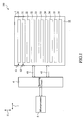
- the touch control device in accordance with the present invention comprises a substrate 1 having a touch control operation surface 11.
- the first electrode group G1 contains a plurality of strip-like electrodes 21, 22, 23, 24, 25, which are spaced from each other by a preset distance that defines an interval area.
- the second electrode group G2 contains a plurality of electrodes 31, 32, 33, 34, 35, which are parallel to the electrodes 21, 22, 23, 24, 25 of the first electrode group G1.
- the electrodes 31, 32, 33, 34, 35 of the second electrode group G2 are respectively set in the interval areas between the electrodes 21, 22, 23, 24, 25 of the first electrode group G1.
- the number of the electrodes contained in each of the first electrode group G1 and the second electrode group G2 is five. However, it is apparent to those having ordinary skills in the art that the number of the electrodes for each of the electrode groups is not limited to the specific number.
- the first electrode group G1 and the second electrode group G2 are respectively connected to a microprocessor 5 via first group scanning lines 41 that are connected to a scanning circuit 4 and second group scanning lines 42 that are connected to the scanning circuit 4.
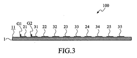
- Figures 2 illustrates a local perspective view of a structure of a touch control pattern that forms the first embodiment touch control device in accordance with the present invention
- Figure 3 is a cross-sectional view taken along line 3-3 of Figure 2 .
- the electrodes 21, 22, 23, 24, 25 of the first electrode group G1 and the electrodes 31, 32, 33, 34, 35 of the second electrode group G2 are set to extend in a first axial direction I and are sequentially and alternately arranged along a second axial direction II.
- the electrodes 21, 22, 23, 24, 25, 31, 32, 33, 34, 35 of the first and second electrode groups G1 and G2 are made of transparent conductive materials, such as ITO that is conventionally used.
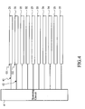
- FIG. 4 shows a schematic circuit diagram of the structure of the touch control pattern of the first embodiment touch control device in accordance with the present invention
- first electrode group G1 an electrode, of which electrode 21 is taken as an example for the following explanation, has an end connected to the scanning circuit 4 via the first group scanning lines 41.
- second electrode group G2 an electrode, of which electrode 31 is taken as an example for the following explanation, has an end connected to the scanning circuit 4 via the second group scanning lines 42.
- the remaining electrodes 22, 23, 24, 25, 32, 33, 34, 35 are also put in connection in a similar way, so that further description is not necessary here.
- the first group scanning lines 41 and the second group scanning lines 42 are made of transparent conductive materials.
- the first group scanning lines 41 and the second group scanning lines 42 are of the functions of “driving” and “scanning” as are employed in the conventional capacitive touch control device, and in the present embodiment, the first group scanning lines 41 and the second group scanning lines 42 are operated to carry out alternate driving and scanning operations.
- the first group scanning lines 41 When the first group scanning lines 41 are operated to carry out driving operation on the electrodes 21, 22, 23, 24, 25 of the first electrode group G1, the second group scanning lines 42 carry out scanning operation on the electrodes 31, 32, 33, 34, 35 of the second electrode group G2; and when the second group scanning lines 42 are operated to carry out driving operation on the electrodes 31, 32, 33, 34, 35 of the second electrode group, the first group scanning lines carry out scanning operation on the electrodes 21, 22, 23, 24, 25 of the first electrode group, in order to detect a touch location of the touch control device 100.
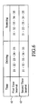
- Figure 5 shows a flow chart of the operation of the touch control device in accordance with the first embodiment of the present invention. As shown, the operation flow of the present embodiment begins with system initialization (step 101).
- step 102 a step of setting scanning mode (step 102) follows.
- the present embodiment includes a single-end sequential scanning mode, and further description will be given for explanation with reference to such a scanning mode.
- the following steps will be explained with additional reference to Figure 6 , which shows a table indicating "driving" and “scanning" operations of the electrodes within different time intervals under the single-end sequential scanning mode.
- the next step is to set a first time interval t1 and a second time interval t2 (step 103).
- the microprocessor 5 employs the first group scanning lines 41 to drive the electrodes 21, 22, 23, 24, 25 of the first electrode group G1 by imposing a driving voltage thereto (step 104).
- the second group scanning lines 42 carries out scanning operation in the single-end sequential scanning mode on a given end of each electrode 31, 32, 33, 34, 35 of the second electrode group G2, such as end 31a, 32a, 33a, 34a, 35a (step 105).
- the microprocessor 5 employs the second group scanning lines 42 to drive the electrodes 31, 32, 33, 34, 35 of the second electrode group G2 (step 106).
- the first group scanning lines 41 carries out scanning operation in the single-end sequential scanning mode on a given end of each electrode 21, 22, 23, 24, 25 of the first electrode group G1, such as end 21a, 22a, 23a, 24a, 25a (step 107).
- the microprocessor 5 can calculate out coordinates of a touch location based on a divided voltage detected at each electrode 21, 22, 23, 24, 25, 31, 32, 33, 34, 35.
Landscapes
- Engineering & Computer Science (AREA)
- General Engineering & Computer Science (AREA)
- Theoretical Computer Science (AREA)
- Human Computer Interaction (AREA)
- Physics & Mathematics (AREA)
- General Physics & Mathematics (AREA)
- Position Input By Displaying (AREA)
- Electronic Switches (AREA)
Applications Claiming Priority (1)
| Application Number | Priority Date | Filing Date | Title |
|---|---|---|---|
| TW097117524A TW200947030A (en) | 2008-05-13 | 2008-05-13 | Capacitive touch control device and method thereof |
Publications (2)
| Publication Number | Publication Date |
|---|---|
| EP2120341A2 true EP2120341A2 (de) | 2009-11-18 |
| EP2120341A3 EP2120341A3 (de) | 2012-08-22 |
Family
ID=40397744
Family Applications (1)
| Application Number | Title | Priority Date | Filing Date |
|---|---|---|---|
| EP08015387A Withdrawn EP2120341A3 (de) | 2008-05-13 | 2008-09-01 | Kapazitative Berührungssteuerungsvorrichtung und Verfahren dafür |
Country Status (3)
| Country | Link |
|---|---|
| US (1) | US8487198B2 (de) |
| EP (1) | EP2120341A3 (de) |
| TW (1) | TW200947030A (de) |
Cited By (4)
| Publication number | Priority date | Publication date | Assignee | Title |
|---|---|---|---|---|
| EP2354908A1 (de) * | 2010-02-10 | 2011-08-10 | AU Optronics Corporation | Kapazitive Berührungstafel mit mehreren Zonen |
| DE102014209839A1 (de) * | 2014-01-27 | 2015-07-30 | Shanghai Avic Optoelectronics Co., Ltd. | Tastfeld und Tasterfassungsverfahren für dieses |
| WO2017137484A1 (de) * | 2016-02-11 | 2017-08-17 | Valeo Schalter Und Sensoren Gmbh | Bedienvorrichtung für ein kraftfahrzeug mit kapazitiver annäherungssensorik sowie kraftfahrzeug |
| EP2672365A3 (de) * | 2012-06-05 | 2017-11-29 | Acer Incorporated | Ansteuerverfahren für einen Berührungsbildschirm und berührungsempfindliche Vorrichtung dafür |
Families Citing this family (37)
| Publication number | Priority date | Publication date | Assignee | Title |
|---|---|---|---|---|
| US7812827B2 (en) * | 2007-01-03 | 2010-10-12 | Apple Inc. | Simultaneous sensing arrangement |
| US8493331B2 (en) | 2007-06-13 | 2013-07-23 | Apple Inc. | Touch detection using multiple simultaneous frequencies |
| US9606663B2 (en) | 2008-09-10 | 2017-03-28 | Apple Inc. | Multiple stimulation phase determination |
| US9348451B2 (en) | 2008-09-10 | 2016-05-24 | Apple Inc. | Channel scan architecture for multiple stimulus multi-touch sensor panels |
| US8592697B2 (en) | 2008-09-10 | 2013-11-26 | Apple Inc. | Single-chip multi-stimulus sensor controller |
| JP5670124B2 (ja) | 2010-08-23 | 2015-02-18 | 株式会社ジャパンディスプレイ | タッチ検出機能付き表示装置、駆動回路、タッチ検出機能付き表示装置の駆動方法および電子機器 |
| JP5667824B2 (ja) | 2010-09-24 | 2015-02-12 | 株式会社ジャパンディスプレイ | タッチ検出装置およびその駆動方法、タッチ検出機能付き表示装置、ならびに電子機器 |
| TWI446253B (zh) | 2011-04-08 | 2014-07-21 | Elan Microelectronics Corp | Single - layer sensing layer of two - dimensional capacitive touchpad |
| CN104169850B (zh) | 2012-01-12 | 2017-06-06 | 辛纳普蒂克斯公司 | 单层电容性成像传感器 |
| KR101570455B1 (ko) | 2012-12-19 | 2015-11-19 | 엘지디스플레이 주식회사 | 터치스크린 일체형 표시장치 및 그 구동 방법 |
| US9552089B2 (en) | 2013-08-07 | 2017-01-24 | Synaptics Incorporated | Capacitive sensing using a matrix electrode pattern |
| TWI512564B (zh) * | 2013-08-30 | 2015-12-11 | Mstar Semiconductor Inc | 感測電極的感測方法與感測裝置 |
| US9298325B2 (en) | 2013-09-30 | 2016-03-29 | Synaptics Incorporated | Processing system for a capacitive sensing device |
| US20150091842A1 (en) | 2013-09-30 | 2015-04-02 | Synaptics Incorporated | Matrix sensor for image touch sensing |
| US10042489B2 (en) | 2013-09-30 | 2018-08-07 | Synaptics Incorporated | Matrix sensor for image touch sensing |
| US9459367B2 (en) | 2013-10-02 | 2016-10-04 | Synaptics Incorporated | Capacitive sensor driving technique that enables hybrid sensing or equalization |
| US9274662B2 (en) | 2013-10-18 | 2016-03-01 | Synaptics Incorporated | Sensor matrix pad for performing multiple capacitive sensing techniques |
| US9495046B2 (en) | 2013-10-23 | 2016-11-15 | Synaptics Incorporated | Parasitic capacitance filter for single-layer capacitive imaging sensors |
| US9081457B2 (en) | 2013-10-30 | 2015-07-14 | Synaptics Incorporated | Single-layer muti-touch capacitive imaging sensor |
| CN104635971B (zh) * | 2013-11-13 | 2017-07-11 | 晨星半导体股份有限公司 | 感测电极的感测方法与感测装置 |
| KR20150062714A (ko) * | 2013-11-29 | 2015-06-08 | 삼성전기주식회사 | 터치스크린 장치 |
| US9798429B2 (en) | 2014-02-28 | 2017-10-24 | Synaptics Incorporated | Guard electrodes in a sensing stack |
| US10133421B2 (en) | 2014-04-02 | 2018-11-20 | Synaptics Incorporated | Display stackups for matrix sensor |
| US9927832B2 (en) | 2014-04-25 | 2018-03-27 | Synaptics Incorporated | Input device having a reduced border region |
| US9690397B2 (en) | 2014-05-20 | 2017-06-27 | Synaptics Incorporated | System and method for detecting an active pen with a matrix sensor |
| US10175827B2 (en) | 2014-12-23 | 2019-01-08 | Synaptics Incorporated | Detecting an active pen using a capacitive sensing device |
| US10795471B2 (en) | 2015-01-05 | 2020-10-06 | Synaptics Incorporated | Modulating a reference voltage to perform capacitive sensing |
| US9939972B2 (en) | 2015-04-06 | 2018-04-10 | Synaptics Incorporated | Matrix sensor with via routing |
| US9720541B2 (en) | 2015-06-30 | 2017-08-01 | Synaptics Incorporated | Arrangement of sensor pads and display driver pads for input device |
| US10095948B2 (en) | 2015-06-30 | 2018-10-09 | Synaptics Incorporated | Modulation scheme for fingerprint sensing |
| US9715304B2 (en) | 2015-06-30 | 2017-07-25 | Synaptics Incorporated | Regular via pattern for sensor-based input device |
| CN205028263U (zh) | 2015-09-07 | 2016-02-10 | 辛纳普蒂克斯公司 | 一种电容传感器 |
| US10037112B2 (en) | 2015-09-30 | 2018-07-31 | Synaptics Incorporated | Sensing an active device'S transmission using timing interleaved with display updates |
| US10067587B2 (en) | 2015-12-29 | 2018-09-04 | Synaptics Incorporated | Routing conductors in an integrated display device and sensing device |
| CN106933400B (zh) | 2015-12-31 | 2021-10-29 | 辛纳普蒂克斯公司 | 单层传感器图案和感测方法 |
| US11648753B2 (en) * | 2016-07-20 | 2023-05-16 | Saint-Gobain Glass France | Window pane having a capacitive switching region for contactlessly controlling a function |
| CN114511888B (zh) * | 2020-11-16 | 2025-08-12 | 群创光电股份有限公司 | 操作感测电路的方法 |
Family Cites Families (20)
| Publication number | Priority date | Publication date | Assignee | Title |
|---|---|---|---|---|
| US4758830A (en) * | 1984-10-25 | 1988-07-19 | Ti Corporate Services Limited | Switch/display units |
| US4839634A (en) * | 1986-12-01 | 1989-06-13 | More Edward S | Electro-optic slate for input/output of hand-entered textual and graphic information |
| US5283556A (en) * | 1988-12-19 | 1994-02-01 | Sharp Kabushiki Kaisha | Tablet integrated with display |
| JP2534422B2 (ja) * | 1991-03-12 | 1996-09-18 | シャープ株式会社 | 表示一体型タブレット装置 |
| EP0644505B1 (de) * | 1993-09-17 | 2000-03-08 | Hitachi, Ltd. | Anzeigegerät mit Koordinateneingabevorrichtung |
| JP3678801B2 (ja) * | 1995-08-02 | 2005-08-03 | シャープ株式会社 | 表示一体型タブレット装置 |
| JP2001075074A (ja) | 1999-08-18 | 2001-03-23 | Internatl Business Mach Corp <Ibm> | タッチセンサ一体型液晶表示素子 |
| JP3959454B2 (ja) * | 2001-10-22 | 2007-08-15 | シャープ株式会社 | 入力装置および入出力装置 |
| US6825833B2 (en) * | 2001-11-30 | 2004-11-30 | 3M Innovative Properties Company | System and method for locating a touch on a capacitive touch screen |
| US6980202B2 (en) * | 2001-12-21 | 2005-12-27 | International Business Machines Corporation | Method and system for creating and accessing hyperlinks from annotations relating to a physical document |
| US6961049B2 (en) * | 2002-06-21 | 2005-11-01 | 3M Innovative Properties Company | Capacitive touch sensor architecture with unique sensor bar addressing |
| US6970160B2 (en) * | 2002-12-19 | 2005-11-29 | 3M Innovative Properties Company | Lattice touch-sensing system |
| TWI240208B (en) * | 2004-02-17 | 2005-09-21 | Elan Microelectronics Corp | Capacitance touch panel with simplified scanning lines and the detection method thereof |
| US20050219229A1 (en) * | 2004-04-01 | 2005-10-06 | Sony Corporation | Image display device and method of driving image display device |
| US7598949B2 (en) * | 2004-10-22 | 2009-10-06 | New York University | Multi-touch sensing light emitting diode display and method for using the same |
| KR20060062164A (ko) * | 2004-12-03 | 2006-06-12 | 삼성전자주식회사 | 광센서를 내장하는 표시 장치 |
| US8144125B2 (en) * | 2006-03-30 | 2012-03-27 | Cypress Semiconductor Corporation | Apparatus and method for reducing average scan rate to detect a conductive object on a sensing device |
| TW200805128A (en) | 2006-05-05 | 2008-01-16 | Harald Philipp | Touch screen element |
| US8009146B2 (en) * | 2007-06-28 | 2011-08-30 | Nokia Corporation | Method, apparatus and computer program product for facilitating data entry via a touchscreen |
| US20090079707A1 (en) * | 2007-09-24 | 2009-03-26 | Motorola, Inc. | Integrated capacitive sensing devices and methods |
-
2008
- 2008-05-13 TW TW097117524A patent/TW200947030A/zh unknown
- 2008-08-13 US US12/222,614 patent/US8487198B2/en active Active
- 2008-09-01 EP EP08015387A patent/EP2120341A3/de not_active Withdrawn
Non-Patent Citations (1)
| Title |
|---|
| None * |
Cited By (7)
| Publication number | Priority date | Publication date | Assignee | Title |
|---|---|---|---|---|
| EP2354908A1 (de) * | 2010-02-10 | 2011-08-10 | AU Optronics Corporation | Kapazitive Berührungstafel mit mehreren Zonen |
| US8780071B2 (en) | 2010-02-10 | 2014-07-15 | Au Optronics Corporation | Capacitive touch panel with multiple zones |
| EP2672365A3 (de) * | 2012-06-05 | 2017-11-29 | Acer Incorporated | Ansteuerverfahren für einen Berührungsbildschirm und berührungsempfindliche Vorrichtung dafür |
| DE102014209839A1 (de) * | 2014-01-27 | 2015-07-30 | Shanghai Avic Optoelectronics Co., Ltd. | Tastfeld und Tasterfassungsverfahren für dieses |
| US9703428B2 (en) | 2014-01-27 | 2017-07-11 | Shanghai Avic Optoelectronics Co., Ltd. | Touch panel and touch detecting method therefor |
| DE102014209839B4 (de) | 2014-01-27 | 2021-12-30 | Shanghai Avic Optoelectronics Co., Ltd. | Tastfeld und Tasterfassungsverfahren für dieses |
| WO2017137484A1 (de) * | 2016-02-11 | 2017-08-17 | Valeo Schalter Und Sensoren Gmbh | Bedienvorrichtung für ein kraftfahrzeug mit kapazitiver annäherungssensorik sowie kraftfahrzeug |
Also Published As
| Publication number | Publication date |
|---|---|
| TWI379115B (de) | 2012-12-11 |
| EP2120341A3 (de) | 2012-08-22 |
| US8487198B2 (en) | 2013-07-16 |
| TW200947030A (en) | 2009-11-16 |
| US20090283340A1 (en) | 2009-11-19 |
Similar Documents
| Publication | Publication Date | Title |
|---|---|---|
| US8487198B2 (en) | Capacitive touch control device and method thereof | |
| CN101593065B (zh) | 电容式触控装置及其方法 | |
| CN201078769Y (zh) | 电容式触控板的触控图型结构 | |
| US8217902B2 (en) | Conductor pattern structure of capacitive touch panel | |
| US8194047B2 (en) | Multi-channel touch panel | |
| EP2650765B1 (de) | Leitermusterstruktur eines kapazitiven Berührungsbildschirms | |
| KR20120037295A (ko) | 터치 패널 | |
| US8605050B2 (en) | Conductor pattern structure of capacitive touch panel | |
| CN106383608B (zh) | 内嵌触摸结构的阵列基板以及显示面板、显示装置 | |
| KR100956973B1 (ko) | 저항막 방식의 멀티 터치 패널 | |
| CN102890589B (zh) | 电容式触控面板的导电图案结构及其构造方法 | |
| CN207424844U (zh) | 简易触摸屏及电子设备 | |
| CN102830869B (zh) | 电容式触控面板的导电图案结构 |
Legal Events
| Date | Code | Title | Description |
|---|---|---|---|
| PUAI | Public reference made under article 153(3) epc to a published international application that has entered the european phase |
Free format text: ORIGINAL CODE: 0009012 |
|
| 17P | Request for examination filed |
Effective date: 20081014 |
|
| AK | Designated contracting states |
Kind code of ref document: A2 Designated state(s): AT BE BG CH CY CZ DE DK EE ES FI FR GB GR HR HU IE IS IT LI LT LU LV MC MT NL NO PL PT RO SE SI SK TR |
|
| AX | Request for extension of the european patent |
Extension state: AL BA MK RS |
|
| PUAL | Search report despatched |
Free format text: ORIGINAL CODE: 0009013 |
|
| AK | Designated contracting states |
Kind code of ref document: A3 Designated state(s): AT BE BG CH CY CZ DE DK EE ES FI FR GB GR HR HU IE IS IT LI LT LU LV MC MT NL NO PL PT RO SE SI SK TR |
|
| AX | Request for extension of the european patent |
Extension state: AL BA MK RS |
|
| RIC1 | Information provided on ipc code assigned before grant |
Ipc: G06F 3/044 20060101ALI20120718BHEP Ipc: H03K 17/96 20060101AFI20120718BHEP |
|
| AKX | Designation fees paid |
Designated state(s): DE FR GB |
|
| STAA | Information on the status of an ep patent application or granted ep patent |
Free format text: STATUS: EXAMINATION IS IN PROGRESS |
|
| 17Q | First examination report despatched |
Effective date: 20180308 |
|
| GRAP | Despatch of communication of intention to grant a patent |
Free format text: ORIGINAL CODE: EPIDOSNIGR1 |
|
| STAA | Information on the status of an ep patent application or granted ep patent |
Free format text: STATUS: GRANT OF PATENT IS INTENDED |
|
| RIC1 | Information provided on ipc code assigned before grant |
Ipc: G06F 3/041 20060101AFI20201022BHEP Ipc: G06F 3/044 20060101ALI20201022BHEP Ipc: H03K 17/96 20060101ALI20201022BHEP |
|
| RAP1 | Party data changed (applicant data changed or rights of an application transferred) |
Owner name: TPK TOUCH SOLUTIONS INC. |
|
| INTG | Intention to grant announced |
Effective date: 20201124 |
|
| STAA | Information on the status of an ep patent application or granted ep patent |
Free format text: STATUS: THE APPLICATION IS DEEMED TO BE WITHDRAWN |
|
| 18D | Application deemed to be withdrawn |
Effective date: 20210407 |