EP2124094A1 - Flüssigkristallanzeigeeinrichtung - Google Patents
Flüssigkristallanzeigeeinrichtung Download PDFInfo
- Publication number
- EP2124094A1 EP2124094A1 EP07850355A EP07850355A EP2124094A1 EP 2124094 A1 EP2124094 A1 EP 2124094A1 EP 07850355 A EP07850355 A EP 07850355A EP 07850355 A EP07850355 A EP 07850355A EP 2124094 A1 EP2124094 A1 EP 2124094A1
- Authority
- EP
- European Patent Office
- Prior art keywords
- recesses
- protrusions
- liquid crystal
- layer
- crystal display
- Prior art date
- Legal status (The legal status is an assumption and is not a legal conclusion. Google has not performed a legal analysis and makes no representation as to the accuracy of the status listed.)
- Withdrawn
Links
Images



Classifications
-
- G—PHYSICS
- G02—OPTICS
- G02F—OPTICAL DEVICES OR ARRANGEMENTS FOR THE CONTROL OF LIGHT BY MODIFICATION OF THE OPTICAL PROPERTIES OF THE MEDIA OF THE ELEMENTS INVOLVED THEREIN; NON-LINEAR OPTICS; FREQUENCY-CHANGING OF LIGHT; OPTICAL LOGIC ELEMENTS; OPTICAL ANALOGUE/DIGITAL CONVERTERS
- G02F1/00—Devices or arrangements for the control of the intensity, colour, phase, polarisation or direction of light arriving from an independent light source, e.g. switching, gating or modulating; Non-linear optics
- G02F1/01—Devices or arrangements for the control of the intensity, colour, phase, polarisation or direction of light arriving from an independent light source, e.g. switching, gating or modulating; Non-linear optics for the control of the intensity, phase, polarisation or colour
- G02F1/13—Devices or arrangements for the control of the intensity, colour, phase, polarisation or direction of light arriving from an independent light source, e.g. switching, gating or modulating; Non-linear optics for the control of the intensity, phase, polarisation or colour based on liquid crystals, e.g. single liquid crystal display cells
- G02F1/133—Constructional arrangements; Operation of liquid crystal cells; Circuit arrangements
- G02F1/1333—Constructional arrangements; Manufacturing methods
- G02F1/1335—Structural association of cells with optical devices, e.g. polarisers or reflectors
- G02F1/133553—Reflecting elements
- G02F1/133555—Transflectors
-
- G—PHYSICS
- G02—OPTICS
- G02F—OPTICAL DEVICES OR ARRANGEMENTS FOR THE CONTROL OF LIGHT BY MODIFICATION OF THE OPTICAL PROPERTIES OF THE MEDIA OF THE ELEMENTS INVOLVED THEREIN; NON-LINEAR OPTICS; FREQUENCY-CHANGING OF LIGHT; OPTICAL LOGIC ELEMENTS; OPTICAL ANALOGUE/DIGITAL CONVERTERS
- G02F1/00—Devices or arrangements for the control of the intensity, colour, phase, polarisation or direction of light arriving from an independent light source, e.g. switching, gating or modulating; Non-linear optics
- G02F1/01—Devices or arrangements for the control of the intensity, colour, phase, polarisation or direction of light arriving from an independent light source, e.g. switching, gating or modulating; Non-linear optics for the control of the intensity, phase, polarisation or colour
- G02F1/13—Devices or arrangements for the control of the intensity, colour, phase, polarisation or direction of light arriving from an independent light source, e.g. switching, gating or modulating; Non-linear optics for the control of the intensity, phase, polarisation or colour based on liquid crystals, e.g. single liquid crystal display cells
- G02F1/133—Constructional arrangements; Operation of liquid crystal cells; Circuit arrangements
- G02F1/1333—Constructional arrangements; Manufacturing methods
- G02F1/133345—Insulating layers
-
- G—PHYSICS
- G02—OPTICS
- G02F—OPTICAL DEVICES OR ARRANGEMENTS FOR THE CONTROL OF LIGHT BY MODIFICATION OF THE OPTICAL PROPERTIES OF THE MEDIA OF THE ELEMENTS INVOLVED THEREIN; NON-LINEAR OPTICS; FREQUENCY-CHANGING OF LIGHT; OPTICAL LOGIC ELEMENTS; OPTICAL ANALOGUE/DIGITAL CONVERTERS
- G02F1/00—Devices or arrangements for the control of the intensity, colour, phase, polarisation or direction of light arriving from an independent light source, e.g. switching, gating or modulating; Non-linear optics
- G02F1/01—Devices or arrangements for the control of the intensity, colour, phase, polarisation or direction of light arriving from an independent light source, e.g. switching, gating or modulating; Non-linear optics for the control of the intensity, phase, polarisation or colour
- G02F1/13—Devices or arrangements for the control of the intensity, colour, phase, polarisation or direction of light arriving from an independent light source, e.g. switching, gating or modulating; Non-linear optics for the control of the intensity, phase, polarisation or colour based on liquid crystals, e.g. single liquid crystal display cells
- G02F1/133—Constructional arrangements; Operation of liquid crystal cells; Circuit arrangements
- G02F1/1333—Constructional arrangements; Manufacturing methods
- G02F1/1335—Structural association of cells with optical devices, e.g. polarisers or reflectors
- G02F1/133553—Reflecting elements
-
- G—PHYSICS
- G02—OPTICS
- G02F—OPTICAL DEVICES OR ARRANGEMENTS FOR THE CONTROL OF LIGHT BY MODIFICATION OF THE OPTICAL PROPERTIES OF THE MEDIA OF THE ELEMENTS INVOLVED THEREIN; NON-LINEAR OPTICS; FREQUENCY-CHANGING OF LIGHT; OPTICAL LOGIC ELEMENTS; OPTICAL ANALOGUE/DIGITAL CONVERTERS
- G02F1/00—Devices or arrangements for the control of the intensity, colour, phase, polarisation or direction of light arriving from an independent light source, e.g. switching, gating or modulating; Non-linear optics
- G02F1/01—Devices or arrangements for the control of the intensity, colour, phase, polarisation or direction of light arriving from an independent light source, e.g. switching, gating or modulating; Non-linear optics for the control of the intensity, phase, polarisation or colour
- G02F1/13—Devices or arrangements for the control of the intensity, colour, phase, polarisation or direction of light arriving from an independent light source, e.g. switching, gating or modulating; Non-linear optics for the control of the intensity, phase, polarisation or colour based on liquid crystals, e.g. single liquid crystal display cells
- G02F1/133—Constructional arrangements; Operation of liquid crystal cells; Circuit arrangements
- G02F1/136—Liquid crystal cells structurally associated with a semi-conducting layer or substrate, e.g. cells forming part of an integrated circuit
- G02F1/1362—Active matrix addressed cells
-
- G—PHYSICS
- G02—OPTICS
- G02F—OPTICAL DEVICES OR ARRANGEMENTS FOR THE CONTROL OF LIGHT BY MODIFICATION OF THE OPTICAL PROPERTIES OF THE MEDIA OF THE ELEMENTS INVOLVED THEREIN; NON-LINEAR OPTICS; FREQUENCY-CHANGING OF LIGHT; OPTICAL LOGIC ELEMENTS; OPTICAL ANALOGUE/DIGITAL CONVERTERS
- G02F2202/00—Materials and properties
- G02F2202/10—Materials and properties semiconductor
Definitions
- the present invention relates to a reflection-type or transflective-type liquid crystal display device capable of performing display by utilizing reflected light.
- Liquid crystal display devices include the transmission-type liquid crystal display device which utilizes backlight from behind the display panel as a light source for displaying, the reflection-type liquid crystal display device which utilizes reflected light of external light, and the transflective-type liquid crystal display device (reflection/transmission-type liquid crystal display device) which utilizes both reflected light of external light and backlight.
- the reflection-type liquid crystal display device and the transflective-type liquid crystal display device are characterized in that they have smaller power consumptions than that of the transmission-type liquid crystal display device, and their displayed images are easy to see in a bright place.
- the transflective-type liquid crystal display device is characterized in that its screen is easier to see than that of the reflection-type liquid crystal display device, even in a dark place.
- FIG. 10 is a cross-sectional view showing an active matrix substrate 100 in a conventional reflection-type liquid crystal display device (e.g., Patent Document 1).
- a conventional reflection-type liquid crystal display device e.g., Patent Document 1.
- the active matrix substrate 100 includes an insulative substrate 101, as well as a gate layer 102, a gate insulating layer 104, a semiconductor layer 106, a metal layer 108, and a reflective layer 110, which are stacked on the insulative substrate 101.
- the gate layer 102, the gate insulating layer 104, the semiconductor layer 106, and the metal layer 108 are subjected to etching by using one mask, thus being formed so as to have an islandlike multilayer structure.
- the reflective layer 110 is formed on this multilayer structure, whereby a reflection surface 112 having ruggednesses is formed.
- transparent electrodes, a liquid crystal layer, a color filter substrate (CF substrate), and the like are stacked above the active matrix substrate 100.
- FIG. 11 is a cross-sectional view of a conventional transflective-type liquid crystal display device (e.g., Patent Document 2).
- an interlayer insulating film 204 is formed on a drain electrode 222 of a switching element (TFT) 203, and a galvanic corrosion preventing film 205, a reflection electrode film 206, and an amorphous transparent electrode film 218 are stacked on the interlayer insulating film 204.
- the region where the reflection electrode film 206 is formed is a reflection region of the transflective-type liquid crystal display device.
- Ruggednesses are formed in an upper portion of the interlayer insulating film 204 within the reflection region, and conforming to these ruggednesses, ruggednesses are also formed on the galvanic corrosion preventing film 205, the reflection electrode film 206, and the amorphous transparent electrode film 218.
- Patent Document 3 describes a liquid crystal display device in which some of the ruggednesses are disposed irregularly in order to suppress occurrence of such a diffraction pattern or the like.
- portions of the reflective layer 110 are formed so as to reach the insulative substrate 101 in portions where the gate layer 102 and the like are not formed (i.e., portions between the islands, hereinafter referred to as "gap portions"). Therefore, in the gap portions, the surface of the reflection surface 112 is recessed in the direction of the insulative substrate 101, thus forming a plane having deep dents (or recesses).
- the reflection-type liquid crystal display device or the transflective-type liquid crystal display device in order to perform bright display with a wide viewing angle, it is necessary to allow incident light entering the display device to be more uniformly and efficiently reflected by the reflection surface 112 across the entire display surface, without causing specular reflection in one direction. For this purpose, it is better if the reflection surface 112 has moderate ruggednesses rather than being a complete plane.
- the reflection surface 112 of the aforementioned active matrix substrate 100 has deep dents. Therefore, light is unlikely to reach the reflection surface located in lower portions of the dents, and even if at all light reaches there, the reflected light thereof is unlikely to be reflected toward the liquid crystal layer, thus resulting in a problem in that the reflected light is not effectively utilized for displaying. Furthermore, many portions of the reflection surface 112 have a large angle with respect to the display surface of the liquid crystal display device, thus resulting in a problem in that so that the reflected light from those portions is not effectively utilized for displaying.
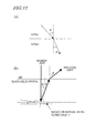
- FIG. 12 is a diagram showing a relationship between the tilt of the reflection surface 112 and reflected light.
- FIG. 12(a) shows a relationship between an incident angle ⁇ and an outgoing angle ⁇ when light enters a medium b having a refractive index Nb from a medium a having a refractive index Na.
- N ⁇ a ⁇ sin ⁇ ⁇ N ⁇ b ⁇ sin ⁇ ⁇
- FIG. 12(b) is a diagram showing a relationship between incident light and reflected light when incident light perpendicularly entering the display surface of a liquid crystal display device is reflected from a reflection surface which is tilted by ⁇ with respect to the display surface (or the substrate). As shown in the figure, the incident light perpendicularly entering the display surface is reflected from the reflection surface which is tilted by angle ⁇ with respect to the display surface, and goes out in a direction of an outgoing angle ⁇ .
- the reflection surface 112 of the aforementioned active matrix substrate 100 has many portions which are greater than 20 degrees, reflected light is not very effectively used for displaying.
- a step of forming an insulating layer and a step of forming contact holes for connecting the reflective layer 110 to the drains of the TFTs in the insulating layer are needed, thus resulting in a problem of an increase in the material and the number of steps.
- the conventional transflective-type liquid crystal display device also has a problem in that the material and number of steps are increased for forming the reflection region.
- the present invention has been made in view of the above problems, and an objective thereof is to provide at low cost reflection-type and transflective-type liquid crystal display devices having a high image quality, in which moiré or coloration due to interference of reflected light and the like is reduced.
- a liquid crystal display device is a liquid crystal display device having a plurality of pixels, and comprising, in each of the plurality of pixels, a reflection region for reflecting incident light toward a display surface, wherein, the reflection region includes a metal layer, a semiconductor layer formed on the metal layer, and a reflective layer formed on the semiconductor layer; a plurality of first recesses or protrusions and a plurality of second recesses or protrusions are formed on a surface of the reflective layer; the plurality of first recesses or protrusions are formed so as to conform to the shapes of recesses (including apertures) or protrusions of the metal layer, and the plurality of second recesses or protrusions are formed so as to conform to the shapes of recesses (including apertures) or protrusions of the semiconductor layer; and the plurality of first recesses or protrusions have a plurality of first pairs of first recesses or protrusions adjoining along a first direction, the plurality of first pairs including
- the plurality of first recesses or protrusions have a plurality of third pairs of first recesses or protrusions adjoining along a third direction which is different from the first direction, and the plurality of third pairs include two pairs whose intervals between recesses or protrusions are different from each other.
- the plurality of second recesses or protrusions have a plurality of fourth pairs of second recesses or protrusions adjoining along a fourth direction which is different from the second direction, and the plurality of fourth pairs include two pairs whose intervals between recesses or protrusions are different from each other.
- the plurality of first recesses or protrusions have a plurality of third pairs of first recesses or protrusions adjoining along a third direction which is different from the first direction, and the plurality of third pairs include two pairs whose intervals between recesses or protrusions are different from each other; and the plurality of second recesses or protrusions have a plurality of fourth pairs of second recesses or protrusions adjoining along a fourth direction which is different from the second direction, and the plurality of fourth pairs include two pairs whose intervals between recesses or protrusions are different from each other.
- At least either the plurality of first recesses or protrusions or the plurality of second recesses or protrusions are randomly disposed.
- both the plurality of first recesses or protrusions and the plurality of second recesses or protrusions are randomly disposed.
- One embodiment comprises a semiconductor element provided corresponding to each of the plurality of pixels, wherein, the metal layer, the semiconductor layer, and the reflective layer are made of same materials as those of a gate electrode, a semiconductor portion, and source and drain electrodes of the semiconductor element, respectively.
- One embodiment comprises a liquid crystal layer and an interlayer insulating layer and a pixel electrode interposed between the liquid crystal layer and the reflective layer, wherein a surface of the pixel electrode facing the liquid crystal layer is formed flat without conforming to shapes of the first recesses or protrusions and the second recesses or protrusions of the reflective layer.
- reflection-type and transflective-type liquid crystal display devices having a high image quality, in which moiré or coloration due to interference of reflected light and the like is reduced, can be provided at low cost.
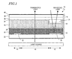
- FIG. 1 is a diagram schematically showing a cross-sectional shape of a liquid crystal display device 10 of the present embodiment.
- the liquid crystal display device 10 is a transflective-type liquid crystal display device (LCD) by an active matrix method.
- the liquid crystal display device 10 includes a TFT (Thin Film Transistor) substrate 12, a counter substrate 14 such as a color filter substrate (CF substrate), and a liquid crystal layer 18 containing liquid crystal 16 which is sealed between the TFT substrate 12 and the counter substrate 14.
- TFT Thin Film Transistor
- CF substrate color filter substrate
- the TFT substrate 12 includes a transparent substrate 22, an interlayer insulating layer 26, and a pixel electrode 28, and includes reflection sections 30 and TFT sections 32. Note that gate lines (scanning lines), source lines (signal lines), Cs lines (storage capacitor electrode lines), and the like are also formed on the TFT substrate 12, which will be described later.
- the counter substrate 14 includes a counter electrode 34, a color filter layer (CF layer) 36, and a transparent substrate 38.
- the upper face of the transparent substrate 38 serves as a display surface 40 of the liquid crystal display device. Note that although the TFT substrate 12 and the counter substrate 14 each have an alignment film and a polarizer, they are omitted from the figure.
- a region where a reflection section 30 is formed is referred to as a reflection region 42, whereas a region where a TFT section 32 is formed is referred to as a TFT region 44.
- the reflection region light entering from the display surface 40 is reflected by the reflection section 30, and travels through the liquid crystal layer 18 and the counter substrate 14 so as to go out from the display surface 40.
- the liquid crystal display device 10 has transmission regions 46 which are formed in regions other than the reflection regions 42 and the TFT regions 44. In the transmission regions 46, light which is emitted from a light source in the liquid crystal display device 10 travels through the TFT substrate 12, the liquid crystal layer 18, and the counter substrate 14 so as to go out from the display surface 40.
- FIG. 1 illustrates the layer 31 as being formed between the counter electrode 34 and the CF layer 36, the layer 31 may be formed on the face of the counter electrode 34 facing the liquid crystal layer 18.
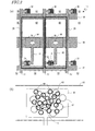
- FIG. 2 is plan views more specifically showing the construction of the pixel regions and the reflection sections 30 of the liquid crystal display device 10.
- FIG. 2(a) is a plan view of a portion of the liquid crystal display device 10, as seen from above the display surface 40. As shown in the figure, a plurality of pixels 50 are disposed in a matrix shape in the liquid crystal display device 10. The aforementioned reflection section 30 and TFT section 32 are formed in each pixel 50, with a TFT being formed in the TFT section 32.
- source lines 52 extend along the column direction (up-down direction in the figure), and gate lines (also referred to as gate metal layers) 54 extend along the row direction (right-left direction in the figure).
- gate lines also referred to as gate metal layers
- a Cs line 56 extends along the row direction.
- a contact hole 58 for connecting the pixel electrode 28 and the drain electrode of the TFT is formed.
- FIG. 2(b) is a plan view schematically showing the construction of the reflection section 30 above the Cs metal layer 56.
- the contact hole 58 is omitted from illustration.
- the reflection section 30 includes a gate insulating layer 61 formed on the Cs metal layer 56, a semiconductor layer 62 formed on the gate insulating layer 61, and a reflective layer 63 formed on the semiconductor layer 62.
- a plurality of protrusions 67 and recesses 68 are provided on the surface of the reflective layer 63. Although 18 recesses 68 and 11 protrusions 67 are illustrated herein for ease of understanding the construction, more recesses 68 may actually be formed.
- the plurality of recesses 68 are formed so as to conform to the shapes of the apertures (or recesses) 65 in the Cs metal layer 56, whereas the protrusion 67 are formed so as to conform to the shapes of the semiconductor layer 62, which is formed in island shapes.
- the Cs metal layer 56 may be formed in island shapes, and protrusions may be formed so as to conform to their shapes, instead of apertures (or recesses) 65. Apertures (or recesses) may be formed in a semiconductor layer 62 which is formed so as to cover the reflection section 30, and recesses may be formed so as to conform to their shapes, instead of protrusions 67.
- any recess 68 or a protrusion replacing it will be referred to as a first recess or protrusion
- any protrusion 67 or a recess replacing it will be referred to as a second recess or protrusion.
- the recesses 68 (or first recesses or protrusions) and the protrusions 67 (or second recesses or protrusions) are both randomly disposed.
- the protrusions 67 and the recesses 68 do not need to be perfectly randomly disposed, but may be randomly disposed in portions of the surface of the reflective layer 63.
- a layout lacking symmetry or an anisotropic layout may be adopted.
- a plurality of pairs (first pairs) of recesses 68 adjoining along a direction (first direction) include two pairs whose intervals between recesses 68 are different from each other.
- a plurality of pairs (second pairs) of protrusions 67 adjoining along a direction (second direction) include two pairs whose intervals between protrusions 67 are different from each other.
- a plurality of pairs (third pairs) of recesses 68 adjoining along a direction (third direction) which is different from the first direction may include two pairs whose intervals between recesses 68 are different from each other, and a plurality of pairs (fourth pairs) of protrusions 67 adjoining along a direction (fourth direction) which is different from the second direction may include two pairs whose intervals between protrusions 67 are different from each other.
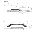
- FIG. 3 (a) shows a cross section of the reflection section 30 (a cross section of a portion shown by arrow B in FIG. 2(b) ).
- the Cs metal layer (metal layer) 56, the gate insulating layer (insulating layer) 61, the semiconductor layer 62, and the reflective layer 63 are stacked.
- the semiconductor layer 62 is composed of an intrinsic amorphous silicon layer (Si(i) layer) and an n+ amorphous silicon layer (Si(n+) layer) which is doped with phosphorus, for example.
- the Cs metal layer 56 has an aperture 65, such that a portion of the semiconductor layer 62, which is formed in an island shape, is located inside the aperture 65.
- a recess 68 is formed on the surface of the reflective layer 63 above the aperture 65, whereas a protrusion 67 is formed on the surface of the reflective layer 63 above the semiconductor layer 62.
- the portion of the surface of the reflective layer 63 where no underlying semiconductor layer 62 is formed becomes a recess 69.
- Level differences are formed in the reflective layer 63 on the semiconductor layer 62 inside the recess 68.
- the recess 68 is formed by the gate insulating layer 61, the semiconductor layer 62, and the reflective layer 63 being formed above the aperture 65 of the Cs metal layer 56, whereby the reflective layer 63 becomes dented.
- the protrusion 67 is created by the reflective layer 63 being formed on the semiconductor layer 62, whereby the reflective layer 63 protrudes.
- a recess (dent) may be formed in the Cs metal layer 56, instead of an aperture 65. In that case, the recess 68 is to be formed in accordance with that recess of the Cs metal layer.
- a level difference may be introduced to the slope of the recess 68.
- a level difference may be introduced to the slope of the protrusion 67.
- FIG. 3(b) is a diagram showing the construction of the gate metal layer (metal layer) 54, the gate insulating layer 61, the semiconductor layer 62, and the reflective layer 63 in the TFT section 32, and is a cross-sectional view of a portion at arrow A in FIG. 2(a) .
- the gate metal layer 54 in the TFT section 32 is formed concurrently with and from the same member as the Cs metal layer 56 in the reflection section 30.
- the gate insulating layer 61, the semiconductor layer 62, and the reflective layer 63 in the TFT section 32 are formed concurrently with and from the same members as, respectively, the gate insulating layer 61, the semiconductor layer 62, and the reflective layer 63 in the reflection section 30.
- the reflective layer 63 is connected to the drain electrode of the TFT.
- FIG. 4 is cross-sectional views for structural comparison between the reflection section 30 of Embodiment 1 and the reflection section of the conventional liquid crystal display device shown in FIG. 10 .
- FIG. 4 (a) schematically shows the structure of the reflection section 30 of Embodiment 1
- FIG. 4(b) schematically shows the structure of the reflection section of the conventional liquid crystal display device. Note that, in these figures, for simplicity, the slopes of each layer of the reflection section 30 and the slopes of each layer of the conventional liquid crystal display device are illustrated as vertical planes, and the corner portions of each level difference (portions shown by dotted circles in the figure) are illustrated as making perpendicular turns.
- corner portions are illustrated as being perpendicular in FIG. 4
- a face having angles which are larger than 20 degrees (exemplified as 30 degrees in this figure) with respect to the substrate is continuously formed from a plane (with an angle of 0 degrees) which is parallel to the substrate. Therefore, by forming more recesses in the reflection section, it becomes possible to form more faces (effective reflection surfaces) whose angle with respect to the substrate is 20 degrees or less on the surface of the reflective layer.
- the effective reflection surfaces that are formed in a corner portion have various tilting angles which are different from one another, the reflected light will not travel in one fixed direction. Therefore, by forming more recesses, it becomes possible to obtain more reflected light which spans a broad range. Moreover, by increasing the number of recesses and ensuring that the tilting angle of the side face of any recess is 20 degrees or less, more reflected light which spans an even broader range can be obtained.
- FIGS. 4(a) and (b) more recesses and protrusions than in the conventional liquid crystal display device are formed in the reflection section 30 of Embodiment 1. Since more corner portions are therefore formed, it is possible to form more effective reflection surfaces on the surface of the reflective layer 63, whereby more light can be reflected toward the display surface across a broad range. Moreover, the recess 68 and the protrusion 67 are formed in accordance with the shapes to which the Cs metal layer 56 and the semiconductor layer 62 are shaped. Therefore, the shapes, depths, and the slope tilting angles of the recess and protrusion can be easily adjusted during the shaping of the Cs metal layer 56 and the semiconductor layer 62.
- the reflective layer 63 which is located inside the recess 68 in Embodiment 1 is formed above the gate insulating layer 61, or above the gate insulating layer 61 and the semiconductor layer 62.
- the reflective layer inside the recess is directly formed on the glass substrate, via neither the gate insulating layer nor the semiconductor layer. Therefore, the bottom face of the recess 68 of Embodiment 1 is formed so as to be shallower than the bottom face of a recess of the conventional liquid crystal display device. As a result, incident light can be reflected more effectively across a broad range.
- the bottom face of a recess is formed at a deep position, so that the tilting angle of the recess inner surface is large, which makes it difficult to form a large number of effective reflection surfaces having a tilt of 20 degrees or less within the recess.
- this recess is formed by forming the gate layer 102, the gate insulating layer 104, and the semiconductor layer 106, and thereafter altogether removing these layers, it has been difficult to increase the effective reflection surface by controlling the tilting angle of the recess inner surface.
- a recess 68 and a protrusion 67 are formed in accordance with the shapes of the Cs metal layer 56 and the semiconductor layer 62, and therefore the position, size, and shape of the recess 68 and the protrusion 67 can be adjusted when stacking these layers.
- the tilt of the slopes of the recess 68 and the protrusion 67 can be controlled, whereby a larger number of effective reflection surfaces with a tilt or 20 degrees or less can be formed, thus allowing more light to be reflected toward the display surface.
- the faces of the interlayer insulating layer 26 and the pixel electrode 28 that are on the liquid crystal layer 18 side are formed flat without conforming to the shapes of the recesses 68 and the protrusions 67 of the reflective layer 63, similarly to the face of the counter electrode 34 that is on the liquid crystal layer 18 side. Therefore, as compared to the conventional transflective-type liquid crystal display device shown in FIG. 11 , the electric field which is formed across the liquid crystal layer 18 becomes uniform, thus making it possible to uniformly control the orientation of the liquid crystal of the reflection region 42 in a desired direction.
- a liquid crystal display device which has a high transmittance and excellent viewing angle characteristics, with little display unevenness.
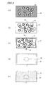
- FIG. 5 is plan views showing a production process, in the reflection region 42, for the TFT substrate 12
- FIG. 6 is cross-sectional views showing a production process, in the reflection region 42, for the TFT substrate 12 (a portion shown at arrow B in FIG. 2(b) ).
- a thin metal film of Al (aluminum) is formed on the transparent substrate 22 having been cleaned.
- this thin metal film may be formed by using Ti (titanium), Cr (chromium), Mo (molybdenum), Ta (tantalum), W (tungsten), or an alloy thereof, etc., or formed from a multilayer body of a layer of such materials and a nitride film.
- a resist film is formed on the thin metal film, and after forming a resist pattern through an exposure-development step, a dry or wet etching is performed to form the Cs metal layer (metal layer) 56 having the apertures 65.
- the thickness of the Cs metal layer 56 is 50 to 1000 nm, for example.
- the apertures 65 are illustrated as being formed in the Cs metal layer 56, a projecting shape of Cs metal layer 56 (or an island-shaped layer) may be formed at the position of each aperture, by using a resist pattern in which the light shielding portions and the transmitting portions are inverted.
- the gate line (gate metal layer) 54 shown in FIG. 2(a) and the gate metal layer 54 of the TFT section 32 shown in FIG. 3(a) are also formed concurrently from the same metal.
- the gate insulating layer 61 composed of SiN (silicon nitride) is formed across the entire substrate surface.
- the gate insulating layer 61 may also be composed of SiO 2 (silicon oxide), Ta 2 O 5 (tantalum oxide), Al 2 O 3 (aluminum oxide), or the like.
- the thickness of the gate insulating layer 61 is 100 to 600 nm, for example.
- the gate insulating layer 61 of the TFT section 32 shown in FIG. 3(b) is also formed concurrently.
- an amorphous silicon (a-Si) film and an n + a-Si film obtained by doping amorphous silicon with phosphorus (P) are formed on the gate insulating layer 61.
- the thickness of the a-Si film is 30 to 300 nm.
- the thickness of the n + a-Si film is 20 to 100 nm.
- these films are shaped by photolithography technique, whereby the semiconductor layer 62 is formed in island shapes. Recess (dents) or apertures may be formed in the semiconductor layer 62 by using a resist pattern in which the light shielding portions and the transmitting portions are inverted.
- the semiconductor layer 62 of the TFT section 32 shown in FIG. 3(b) is also formed concurrently.
- a thin metal film of Al or the like is formed across the entire substrate surface by sputtering technique or the like, thus forming the reflective layer 63.
- the materials which are mentioned above as materials for the Cs metal layer 56 may be used.
- the thickness of the reflective layer 63 is 30 to 1000 nm or less.
- the recess 68 is formed on the surface of the reflective layer 63 above each aperture 65 in the Cs metal layer 56, and the protrusion 67 is formed on the surface of the reflective layer 63 above the semiconductor layer 62.
- the reflective layer 63 of the TFT section 32 shown in FIG. 3(b) is also formed concurrently, and in the TFT section 32, the reflective layer 63 forms a source electrode and a drain electrode of the TFT. Also at this time, the source line 52 in FIG. 2(a) is also formed as a portion of the reflective layer 63.
- a photosensitive acrylic resin is applied by spin-coating, whereby the interlayer insulating layer (interlayer resin layer) 26 is formed.
- the thickness of the interlayer insulating layer 26 is 0.3 to 5 ⁇ m.
- a thin film such as SiN x or SiO 2 may be formed by P-CVD technique as a protection film between the reflective layer 63 and the interlayer insulating layer 26, such is omitted from the figure.
- the thickness of the protection film is 50 to 1000 nm.
- the interlayer insulating layer 26 and the protection film are formed not only on the reflection region 42, but also on the entire upper surface of the transparent substrate 22 including the TFT region 44. Thereafter, through a development process using an exposure apparatus, a contact hole 58 is formed near the center of the reflection section 30.
- a transparent electrode film of ITO, IZO, or the like is formed on the interlayer insulating layer 26 by sputtering technique or the like, and this transparent electrode film is subjected to pattern shaping by photolithography technique, whereby the pixel electrode 28 is formed.
- the pixel electrode 28 is formed not only on the reflection region 42 but also on the entire upper surface of the pixel including the TFT region 44.
- the pixel electrode 28 is formed above the interlayer insulating layer 26 and the contact hole 58, such that the metal member of the pixel electrode 28 is in contact with the reflective layer 63 via the contact hole 58.
- the drain electrode of the TFT in the TFT section 32 is electrically connected to the pixel electrode 28 via the contact hole 58.
- the upper face of the interlayer insulating layer 26 and the surface of the pixel electrode 28 are formed flat without conforming to the shapes of the recesses 68 and the protrusions 67 of the reflective layer 63.
- each aperture in the Cs metal layer 56 and the semiconductor layer 62 is 2 to 17 ⁇ m.
- liquid crystal display device which is capable of performing high-quality displaying with a high luminance, in which reflected light is efficiently utilized and moiré and coloration due to interference of reflected light is reduced.
- the liquid crystal display device of the present embodiment basically has the same construction as that of the liquid crystal display device 10 of Embodiment 1 described above, except only for the layout of the recesses 68 and the protrusions 67 which are formed on the reflection section 30. Therefore, the layout of the recesses 68 and the protrusions 67 will be mainly described below, while omitting the descriptions of any other portions.
- FIG. 7 is a plan view schematically showing the reflection section 30 of the liquid crystal display device according to Embodiment 2, which corresponds to FIG. 2(b) showing the reflection section 30 of Embodiment 1.
- a plurality of protrusions 67 and recesses 68 are formed on the surface of the reflective layer 63 in the reflection section 30, as shown in the figure.
- the Cs metal layer 56 may be formed in island shapes, and protrusions may be formed so as to conform to their shapes, instead of apertures (or recesses) 65.
- Apertures (or recesses) may be formed in the semiconductor layer 62, and recesses may be formed so as to conform to their shapes, instead of protrusions 67.
- recesses 68 are disposed at equal intervals along the vertical direction and along the lateral direction, whereas the protrusions 67 (or second recesses or protrusions) are randomly disposed similarly to Embodiment 1.
- the protrusions 67 do not need to be perfectly randomly disposed, but may be randomly disposed in portions of the surface of the reflective layer 63.
- a layout lacking symmetry or an anisotropic layout may be adopted.
- a plurality of pairs (second pairs) of protrusions 67 adjoining along a direction (second direction) include two pairs whose intervals between protrusions 67 are different from each other.
- a plurality of pairs (fourth pairs) of protrusions 67 adjoining along a direction (fourth direction) which is different from the second direction may include two pairs whose intervals between protrusions 67 are different from each other.
- the liquid crystal display device of the present embodiment basically has the same construction as that of the liquid crystal display device 10 of Embodiment 1 described above, except only for the layout of the recesses 68 and the protrusions 67 which are formed on the reflection section 30. Therefore, the layout of the recesses 68 and the protrusions 67 will be mainly described below, while omitting the descriptions of any other portions.
- FIG. 8 is a plan view schematically showing the reflection section 30 of the liquid crystal display device of Embodiment 3, which corresponds to FIG. 2(b) showing the reflection section 30 of Embodiment 1.
- a plurality of protrusions 67 and recesses 68 are formed on the surface of the reflective layer 63 in the reflection section 30, as shown in the figure.
- the Cs metal layer 56 may be formed in island shapes, and protrusions may be formed so as to conform to their shapes, instead of apertures (or recesses) 65.
- Aperture (or recesses) may be formed in the semiconductor layer 62, and recesses may be formed so as to conform to their shapes, instead of protrusions 67.
- the recesses 68 are randomly disposed similarly to Embodiment 1, whereas the protrusions 67 (or second recesses or protrusions) are disposed at equal intervals along the vertical direction and along the lateral direction.
- the recesses 68 do not need to be perfectly randomly disposed, but may be randomly disposed in portions of the surface of the reflective layer 63.
- a layout lacking symmetry or an anisotropic layout may be adopted.
- a plurality of pairs (first pairs) of recesses 68 adjoining along a direction (first direction) include two pairs whose intervals between recesses 68 are different from each other.
- a plurality of pairs (third pairs) of recesses 68 adjoining along a direction (third direction) which is different from the first direction may include two pairs whose intervals between recesses 68 are different from each other.
- FIG. 9 is a diagram schematically showing a cross-sectional shape of the liquid crystal display device of the present embodiment.
- This liquid crystal display device is based on the liquid crystal display devices of Embodiments 1 to 3 from which the interlayer insulating layer 26 is excluded, and is identical to the liquid crystal display devices of Embodiments 1 to 3 except for the points discussed below. Note that, in FIG. 9 , the detailed structure of the counter substrate 14 and the TFT section 32 are omitted from illustration.
- Embodiment 4 no interlayer insulating layer 26 is formed, and therefore the pixel electrode 28 is formed upon the reflective layer 63 in the reflection section 30 and the TFT section 32, via an insulative film not shown.
- the structure and production method for the reflection section 30 and the TFT section 32 are the same as those which were described in Embodiment 1 except that the interlayer insulating layer 26 is eliminated.
- the pixel layout and wiring structure in the display device are also similar to what is shown in FIG. 2(a) . Also with this construction, similarly to Embodiments 1 to 3, the effective reflection surface of the reflective layer 63 is expanded in area, so that more light can be reflected toward the display surface.
- Embodiments 1 to 4 illustrate that the apertures 65 in the Cs metal layer 56, the semiconductor layer 62, the protrusions 67, and the recesses 68 are circular, but they may be formed into ellipses, polygons such as triangles or rectangles, or formed into various shapes such as recesses or protrusions with sawtoothed edges, or combinations thereof.
- a liquid crystal display device includes a large number of level differences and corner portions on the surface of a reflective layer, as well as a large number of slopes with a tilting angle of 20 degrees or less, and therefore acquires reflection regions with broad effective reflection surfaces and excellent scattering characteristics. Moreover, since the shape of the reflective layer surface is not likely to have symmetry, occurrence of moiré and coloration due to interference of reflected light can be reduced or prevented. Thus, a liquid crystal display device having a high brightness and being capable of clear displaying can be provided.
- the liquid crystal display device according to the present invention is formed by the above-described production method, it can be produced with the same material and the same steps as those of a transmission-type liquid crystal display device. Therefore, a high-quality liquid crystal display device can be provided inexpensively.
- the face of a pixel electrode facing the liquid crystal layer is formed flat, similarly to its face on the counter electrode side, and no level difference is formed in the pixel electrode near the end of the reflection section, thus making it possible to uniformly control the orientation of liquid crystal in a desired direction. Therefore, it is possible to provide a liquid crystal display device which has a high transmittance, excellent viewing angle characteristics, and little display unevenness.
- the liquid crystal display device encompasses display apparatuses, television sets, mobile phones, etc., in which a liquid crystal panel is utilized.
- a liquid crystal panel is utilized.
- the present embodiment employs a transflective-type liquid crystal display device as an example, a reflection-type liquid crystal display device or the like having a configuration similar to the aforementioned reflection section is also encompassed as an embodiment of the present invention.
- a transflective-type liquid crystal display device and a reflection-type liquid crystal display device having a high image quality can be provide inexpensively.
- Liquid crystal display devices according to present invention are suitably used for various liquid crystal display devices, and are suitably used for transflective-type and reflection-type liquid crystal display devices which perform display by utilizing reflected light, e.g., mobile phones, onboard display devices such as car navigation systems, display devices of ATMs and vending machines, etc., portable display devices, laptop PCs, and the like.
Landscapes
- Physics & Mathematics (AREA)
- Nonlinear Science (AREA)
- Mathematical Physics (AREA)
- Chemical & Material Sciences (AREA)
- Crystallography & Structural Chemistry (AREA)
- General Physics & Mathematics (AREA)
- Optics & Photonics (AREA)
- Liquid Crystal (AREA)
Applications Claiming Priority (2)
| Application Number | Priority Date | Filing Date | Title |
|---|---|---|---|
| JP2007021200 | 2007-01-31 | ||
| PCT/JP2007/073787 WO2008093467A1 (ja) | 2007-01-31 | 2007-12-10 | 液晶表示装置 |
Publications (2)
| Publication Number | Publication Date |
|---|---|
| EP2124094A1 true EP2124094A1 (de) | 2009-11-25 |
| EP2124094A4 EP2124094A4 (de) | 2011-09-07 |
Family
ID=39673783
Family Applications (1)
| Application Number | Title | Priority Date | Filing Date |
|---|---|---|---|
| EP07850355A Withdrawn EP2124094A4 (de) | 2007-01-31 | 2007-12-10 | Flüssigkristallanzeigeeinrichtung |
Country Status (5)
| Country | Link |
|---|---|
| US (1) | US20100118238A1 (de) |
| EP (1) | EP2124094A4 (de) |
| JP (1) | JP5048688B2 (de) |
| CN (1) | CN101600987B (de) |
| WO (1) | WO2008093467A1 (de) |
Families Citing this family (16)
| Publication number | Priority date | Publication date | Assignee | Title |
|---|---|---|---|---|
| CN101238408B (zh) * | 2005-08-03 | 2011-06-01 | 夏普株式会社 | 液晶显示装置和具有该液晶显示装置的电子设备 |
| WO2007108268A1 (ja) * | 2006-03-23 | 2007-09-27 | Sharp Kabushiki Kaisha | 液晶表示装置 |
| WO2008001595A1 (fr) * | 2006-06-30 | 2008-01-03 | Sharp Kabushiki Kaisha | Dispositif d'affichage à cristaux liquides et procédé de fabrication du dispositif d'affichage à cristaux liquides |
| JP4927851B2 (ja) | 2006-09-12 | 2012-05-09 | シャープ株式会社 | マイクロレンズアレイ付き液晶表示パネル、その製造方法、および液晶表示装置 |
| WO2008047517A1 (en) * | 2006-10-18 | 2008-04-24 | Sharp Kabushiki Kaisha | Liquid crystal display and method for manufacturing liquid crystal display |
| WO2008047788A1 (en) * | 2006-10-18 | 2008-04-24 | Sharp Kabushiki Kaisha | Liquid crystal display device and method for manufacturing liquid crystal display device |
| JP5284106B2 (ja) * | 2006-12-14 | 2013-09-11 | シャープ株式会社 | 液晶表示装置および液晶表示装置の製造方法 |
| CN101589331B (zh) * | 2007-01-24 | 2011-06-22 | 夏普株式会社 | 液晶显示装置 |
| CN101688993B (zh) * | 2007-06-26 | 2011-09-21 | 夏普株式会社 | 液晶显示装置和液晶显示装置的制造方法 |
| US8872180B2 (en) * | 2008-05-13 | 2014-10-28 | Sharp Kabushiki Kaisha | Liquid crystal display device and method for manufacturing liquid crystal display device |
| JP2016186424A (ja) * | 2015-03-27 | 2016-10-27 | パイオニア株式会社 | 情報取得装置及び固定具 |
| CN109524422B (zh) * | 2019-01-07 | 2024-09-06 | 京东方科技集团股份有限公司 | 阵列基板及其制作方法、反射式显示面板和显示装置 |
| JP7407683B2 (ja) * | 2019-02-22 | 2024-01-04 | パイオニア株式会社 | 情報取得装置 |
| JP2019074542A (ja) * | 2019-02-22 | 2019-05-16 | パイオニア株式会社 | 取得装置 |
| CN210605272U (zh) * | 2019-11-29 | 2020-05-22 | 北京京东方光电科技有限公司 | 显示面板及显示装置 |
| JP2022163125A (ja) * | 2020-09-29 | 2022-10-25 | パイオニア株式会社 | 取得装置 |
Family Cites Families (57)
| Publication number | Priority date | Publication date | Assignee | Title |
|---|---|---|---|---|
| JPS5691277A (en) * | 1979-12-25 | 1981-07-24 | Citizen Watch Co Ltd | Liquiddcrystal display panel |
| JPS58125084A (ja) * | 1982-01-21 | 1983-07-25 | 株式会社東芝 | 液晶表示装置およびその製造方法 |
| DE69220643T2 (de) * | 1991-09-10 | 1998-01-22 | Sharp Kk | Flüssigkristall-Anzeigegerät vom Reflexionstyp und Verfahren zu dessen Herstellung |
| US5418635A (en) * | 1992-02-19 | 1995-05-23 | Sharp Kabushiki Kaisha | Liquid crystal device with a reflective substrate with bumps of photosensitive resin which have 2 or more heights and random configuration |
| JPH06258637A (ja) * | 1993-03-04 | 1994-09-16 | Sony Corp | 液晶表示装置 |
| JP2990046B2 (ja) * | 1995-08-16 | 1999-12-13 | 日本電気株式会社 | 反射型液晶表示装置及びその製造方法 |
| JPH0964366A (ja) * | 1995-08-23 | 1997-03-07 | Toshiba Corp | 薄膜トランジスタ |
| JP3149793B2 (ja) * | 1996-07-22 | 2001-03-26 | 日本電気株式会社 | 反射型液晶表示装置及びその製造方法 |
| KR100392909B1 (ko) * | 1997-08-26 | 2004-03-22 | 엘지.필립스 엘시디 주식회사 | 박막트랜지스터및그의제조방법 |
| JP3666181B2 (ja) * | 1997-03-21 | 2005-06-29 | ソニー株式会社 | 反射型兼透過型表示装置 |
| TW589504B (en) * | 1997-06-12 | 2004-06-01 | Sharp Kk | Liquid crystal display device |
| US6330047B1 (en) * | 1997-07-28 | 2001-12-11 | Sharp Kabushiki Kaisha | Liquid crystal display device and method for fabricating the same |
| JPH11133399A (ja) * | 1997-10-27 | 1999-05-21 | Hitachi Ltd | 反射型液晶表示装置とその製造方法 |
| JP3019831B2 (ja) * | 1998-03-11 | 2000-03-13 | 日本電気株式会社 | 反射型液晶表示装置及びその製造方法 |
| US6839108B1 (en) * | 1998-05-16 | 2005-01-04 | Semiconductor Energy Laboratory Co., Ltd. | Liquid crystal display device and method of manufacturing the same |
| JP2000047200A (ja) * | 1998-07-31 | 2000-02-18 | Hitachi Ltd | 拡散反射板とそれを用いた液晶表示装置およびその製法 |
| US6992718B1 (en) * | 1998-08-31 | 2006-01-31 | Matsushita Electric Industrial Co., Ltd. | Illuminating apparatus, display panel, view finder, video display apparatus, and video camera mounting the elements |
| US6287899B1 (en) * | 1998-12-31 | 2001-09-11 | Samsung Electronics Co., Ltd. | Thin film transistor array panels for a liquid crystal display and a method for manufacturing the same |
| KR100407413B1 (ko) * | 1999-07-19 | 2003-11-28 | 마쯔시다덴기산교 가부시키가이샤 | 반사판 및 그 제조방법, 및 반사판을 구비한 반사형표시소자 및 그 제조방법 |
| US6909481B2 (en) * | 2000-11-07 | 2005-06-21 | Seiko Epson Corporation | Liquid crystal display and electronic appliance |
| TW578028B (en) * | 1999-12-16 | 2004-03-01 | Sharp Kk | Liquid crystal display and manufacturing method thereof |
| JP2001281698A (ja) * | 2000-03-30 | 2001-10-10 | Advanced Display Inc | 電気光学素子の製法 |
| TWI230273B (en) * | 2000-04-17 | 2005-04-01 | Matsushita Electric Industrial Co Ltd | Reflection board, reflection type liquid crystal display unit and production method thereof, optical member, display unit, illuminating device, display board, and undulatory member |
| JP2002014211A (ja) | 2000-04-24 | 2002-01-18 | Matsushita Electric Ind Co Ltd | 反射板、反射型液晶表示装置及びその製造方法、光学部材、表示装置、照明装置、表示板、並びに波動部材 |
| US6747289B2 (en) * | 2000-04-27 | 2004-06-08 | Semiconductor Energy Laboratory Co., Ltd. | Semiconductor device and method of fabricating thereof |
| US6900084B1 (en) * | 2000-05-09 | 2005-05-31 | Semiconductor Energy Laboratory Co., Ltd. | Semiconductor device having a display device |
| JP3712637B2 (ja) * | 2000-08-11 | 2005-11-02 | シャープ株式会社 | 液晶表示装置およびその欠陥修正方法 |
| JP2002062665A (ja) * | 2000-08-16 | 2002-02-28 | Koninkl Philips Electronics Nv | 金属膜の製造方法、該金属膜を有する薄膜デバイス、及び該薄膜デバイスを備えた液晶表示装置 |
| JP3904828B2 (ja) * | 2000-12-07 | 2007-04-11 | 株式会社日立製作所 | 液晶表示装置 |
| TW571165B (en) * | 2000-12-15 | 2004-01-11 | Nec Lcd Technologies Ltd | Liquid crystal display device |
| JP2002184908A (ja) * | 2000-12-19 | 2002-06-28 | Sony Corp | 電子回路装置 |
| JP3875125B2 (ja) * | 2001-04-11 | 2007-01-31 | シャープ株式会社 | 液晶表示装置 |
| JP2002323705A (ja) * | 2001-04-25 | 2002-11-08 | Seiko Epson Corp | 電気光学装置および電子機器 |
| JP4111785B2 (ja) * | 2001-09-18 | 2008-07-02 | シャープ株式会社 | 液晶表示装置 |
| TW517393B (en) * | 2001-11-09 | 2003-01-11 | Prime View Int Co Ltd | TFT LCD structure with protrusion structure and its manufacturing method |
| JP2003222854A (ja) * | 2002-01-31 | 2003-08-08 | Casio Comput Co Ltd | 液晶表示装置およびその製造方法 |
| JP3900975B2 (ja) * | 2002-03-06 | 2007-04-04 | オムロン株式会社 | 反射板、反射型表示装置および電子機器並びに光反射方法および画像表示方法 |
| JP4004835B2 (ja) * | 2002-04-02 | 2007-11-07 | 株式会社アドバンスト・ディスプレイ | 薄膜トランジスタアレイ基板の製造方法 |
| JP4029663B2 (ja) * | 2002-05-22 | 2008-01-09 | セイコーエプソン株式会社 | 半透過反射型液晶装置、およびそれを用いた電子機器 |
| JP4133088B2 (ja) * | 2002-08-01 | 2008-08-13 | Nec液晶テクノロジー株式会社 | 液晶表示装置 |
| JP2005121908A (ja) * | 2003-10-16 | 2005-05-12 | Advanced Display Inc | 反射型液晶表示装置および半透過型液晶表示装置ならびにこれらの製法 |
| JP2005173037A (ja) * | 2003-12-09 | 2005-06-30 | Fujitsu Display Technologies Corp | 液晶表示装置及びその製造方法 |
| JP4338511B2 (ja) * | 2003-12-24 | 2009-10-07 | シャープ株式会社 | 液晶表示装置 |
| JP2005277402A (ja) | 2004-02-25 | 2005-10-06 | Mitsubishi Gas Chem Co Inc | 反射電極膜を含む積層膜のエッチング組成物および積層配線構造の形成方法 |
| SG114747A1 (en) * | 2004-02-25 | 2005-09-28 | Mitsubishi Gas Chemical Co | Etching composition for laminated film including reflective electrode and method for forming laminated wiring structure |
| CN100378554C (zh) * | 2004-04-02 | 2008-04-02 | 统宝光电股份有限公司 | 液晶显示器的制造方法 |
| JP4499481B2 (ja) * | 2004-06-03 | 2010-07-07 | 富士通株式会社 | 液晶表示装置及びその製造方法 |
| JP4606822B2 (ja) * | 2004-09-10 | 2011-01-05 | シャープ株式会社 | 半透過型液晶表示装置の製造方法 |
| JP4578958B2 (ja) * | 2004-12-16 | 2010-11-10 | シャープ株式会社 | 液晶表示装置 |
| KR100648223B1 (ko) * | 2005-05-11 | 2006-11-24 | 비오이 하이디스 테크놀로지 주식회사 | 반투과형 프린지 필드 스위칭 모드 액정표시장치 |
| EP2479604B1 (de) * | 2005-12-05 | 2015-07-15 | Semiconductor Energy Laboratory Co., Ltd. | Flüssigkristallanzeigevorrichtung |
| JP5010586B2 (ja) * | 2006-05-01 | 2012-08-29 | シャープ株式会社 | 液晶表示装置および液晶表示装置の製造方法 |
| JP5010585B2 (ja) * | 2006-05-01 | 2012-08-29 | シャープ株式会社 | 液晶表示装置および液晶表示装置の製造方法 |
| US7847904B2 (en) * | 2006-06-02 | 2010-12-07 | Semiconductor Energy Laboratory Co., Ltd. | Liquid crystal display device and electronic appliance |
| WO2008047517A1 (en) * | 2006-10-18 | 2008-04-24 | Sharp Kabushiki Kaisha | Liquid crystal display and method for manufacturing liquid crystal display |
| WO2008129748A1 (ja) * | 2007-04-13 | 2008-10-30 | Sharp Kabushiki Kaisha | 液晶表示装置、及び液晶表示装置の製造方法 |
| CN101688993B (zh) * | 2007-06-26 | 2011-09-21 | 夏普株式会社 | 液晶显示装置和液晶显示装置的制造方法 |
-
2007
- 2007-12-10 US US12/524,914 patent/US20100118238A1/en not_active Abandoned
- 2007-12-10 WO PCT/JP2007/073787 patent/WO2008093467A1/ja not_active Ceased
- 2007-12-10 CN CN2007800507654A patent/CN101600987B/zh not_active Expired - Fee Related
- 2007-12-10 JP JP2008556014A patent/JP5048688B2/ja not_active Expired - Fee Related
- 2007-12-10 EP EP07850355A patent/EP2124094A4/de not_active Withdrawn
Also Published As
| Publication number | Publication date |
|---|---|
| EP2124094A4 (de) | 2011-09-07 |
| WO2008093467A1 (ja) | 2008-08-07 |
| JPWO2008093467A1 (ja) | 2010-05-20 |
| CN101600987A (zh) | 2009-12-09 |
| US20100118238A1 (en) | 2010-05-13 |
| JP5048688B2 (ja) | 2012-10-17 |
| CN101600987B (zh) | 2011-09-21 |
Similar Documents
| Publication | Publication Date | Title |
|---|---|---|
| EP2124094A1 (de) | Flüssigkristallanzeigeeinrichtung | |
| EP2144109B1 (de) | Flüssigkristallanzeige und verfahren zum herstellen einer flüssigkristallanzeige | |
| EP2128690B1 (de) | Flüssigkristallanzeigevorrichtung | |
| EP2166403A1 (de) | Flüssigkristallanzeigeanordnung und verfahren zur herstellung einer flüssigkristallanzeigeanordnung | |
| US8300186B2 (en) | Liquid crystal display device comprising a reflection region having tilted first and second recesses and method for manufacturing the same | |
| US8421967B2 (en) | Liquid crystal display device and process for producing liquid crystal display device | |
| US8294854B2 (en) | Liquid crystal display comprising a reflection region having first, second and third recesses and method for manufacturing the same | |
| US7528911B2 (en) | Liquid crystal display device and method of manufacturing the same | |
| EP2085813B1 (de) | Flüssigkristallanzeige und verfahren zum herstellen einer flüssigkristallanzeige | |
| US20090122223A1 (en) | Liquid crystal display panel | |
| TW594220B (en) | Liquid crystal display device | |
| US20040212764A1 (en) | Liquid crystal display device | |
| KR100734461B1 (ko) | 액정 표시 장치 | |
| US20090195741A1 (en) | Liquid crystal display and method for manufacturing liquid crystal display | |
| JP2009139853A (ja) | 液晶表示装置 | |
| US7995167B2 (en) | Liquid crystal display device and method for manufacturing liquid crystal display device | |
| US8872180B2 (en) | Liquid crystal display device and method for manufacturing liquid crystal display device | |
| JP2006053303A (ja) | 液晶表示装置 |
Legal Events
| Date | Code | Title | Description |
|---|---|---|---|
| PUAI | Public reference made under article 153(3) epc to a published international application that has entered the european phase |
Free format text: ORIGINAL CODE: 0009012 |
|
| 17P | Request for examination filed |
Effective date: 20090806 |
|
| AK | Designated contracting states |
Kind code of ref document: A1 Designated state(s): AT BE BG CH CY CZ DE DK EE ES FI FR GB GR HU IE IS IT LI LT LU LV MC MT NL PL PT RO SE SI SK TR |
|
| DAX | Request for extension of the european patent (deleted) | ||
| A4 | Supplementary search report drawn up and despatched |
Effective date: 20110810 |
|
| RIC1 | Information provided on ipc code assigned before grant |
Ipc: G02F 1/1335 20060101AFI20110804BHEP Ipc: G02F 1/1368 20060101ALI20110804BHEP |
|
| STAA | Information on the status of an ep patent application or granted ep patent |
Free format text: STATUS: THE APPLICATION HAS BEEN WITHDRAWN |
|
| 18W | Application withdrawn |
Effective date: 20130829 |