EP2124245A1 - Hochpräzises Messinstrument - Google Patents
Hochpräzises Messinstrument Download PDFInfo
- Publication number
- EP2124245A1 EP2124245A1 EP08156665A EP08156665A EP2124245A1 EP 2124245 A1 EP2124245 A1 EP 2124245A1 EP 08156665 A EP08156665 A EP 08156665A EP 08156665 A EP08156665 A EP 08156665A EP 2124245 A1 EP2124245 A1 EP 2124245A1
- Authority
- EP
- European Patent Office
- Prior art keywords
- ion beam
- tip
- supertip
- specimen
- focused ion
- Prior art date
- Legal status (The legal status is an assumption and is not a legal conclusion. Google has not performed a legal analysis and makes no representation as to the accuracy of the status listed.)
- Withdrawn
Links
- 238000005259 measurement Methods 0.000 title claims description 68
- 239000000523 sample Substances 0.000 claims abstract description 155
- 238000010884 ion-beam technique Methods 0.000 claims abstract description 108
- 238000000034 method Methods 0.000 claims abstract description 30
- 239000000463 material Substances 0.000 claims abstract description 29
- 239000013078 crystal Substances 0.000 claims abstract description 12
- 239000007789 gas Substances 0.000 claims description 56
- 125000004429 atom Chemical group 0.000 claims description 20
- BASFCYQUMIYNBI-UHFFFAOYSA-N platinum Chemical compound [Pt] BASFCYQUMIYNBI-UHFFFAOYSA-N 0.000 claims description 13
- 239000011163 secondary particle Substances 0.000 claims description 13
- 238000001514 detection method Methods 0.000 claims description 12
- KDLHZDBZIXYQEI-UHFFFAOYSA-N Palladium Chemical compound [Pd] KDLHZDBZIXYQEI-UHFFFAOYSA-N 0.000 claims description 7
- 238000000605 extraction Methods 0.000 claims description 7
- WFKWXMTUELFFGS-UHFFFAOYSA-N tungsten Chemical compound [W] WFKWXMTUELFFGS-UHFFFAOYSA-N 0.000 claims description 7
- 239000001307 helium Substances 0.000 claims description 6
- 229910052734 helium Inorganic materials 0.000 claims description 6
- 229910052697 platinum Inorganic materials 0.000 claims description 6
- 229910052721 tungsten Inorganic materials 0.000 claims description 6
- 239000010937 tungsten Substances 0.000 claims description 6
- 239000011248 coating agent Substances 0.000 claims description 5
- 238000000576 coating method Methods 0.000 claims description 5
- SWQJXJOGLNCZEY-UHFFFAOYSA-N helium atom Chemical compound [He] SWQJXJOGLNCZEY-UHFFFAOYSA-N 0.000 claims description 5
- XKRFYHLGVUSROY-UHFFFAOYSA-N Argon Chemical compound [Ar] XKRFYHLGVUSROY-UHFFFAOYSA-N 0.000 claims description 4
- 239000001257 hydrogen Substances 0.000 claims description 4
- 229910052739 hydrogen Inorganic materials 0.000 claims description 4
- 125000004435 hydrogen atom Chemical class [H]* 0.000 claims description 4
- 229910052754 neon Inorganic materials 0.000 claims description 4
- GKAOGPIIYCISHV-UHFFFAOYSA-N neon atom Chemical compound [Ne] GKAOGPIIYCISHV-UHFFFAOYSA-N 0.000 claims description 4
- 229910052751 metal Inorganic materials 0.000 claims description 3
- 239000002184 metal Substances 0.000 claims description 3
- 229910052763 palladium Inorganic materials 0.000 claims description 3
- ZOKXTWBITQBERF-UHFFFAOYSA-N Molybdenum Chemical compound [Mo] ZOKXTWBITQBERF-UHFFFAOYSA-N 0.000 claims description 2
- 229910052786 argon Inorganic materials 0.000 claims description 2
- 229910052741 iridium Inorganic materials 0.000 claims description 2
- GKOZUEZYRPOHIO-UHFFFAOYSA-N iridium atom Chemical compound [Ir] GKOZUEZYRPOHIO-UHFFFAOYSA-N 0.000 claims description 2
- 229910052750 molybdenum Inorganic materials 0.000 claims description 2
- 239000011733 molybdenum Substances 0.000 claims description 2
- 229910052758 niobium Inorganic materials 0.000 claims description 2
- 239000010955 niobium Substances 0.000 claims description 2
- GUCVJGMIXFAOAE-UHFFFAOYSA-N niobium atom Chemical compound [Nb] GUCVJGMIXFAOAE-UHFFFAOYSA-N 0.000 claims description 2
- 229910052702 rhenium Inorganic materials 0.000 claims description 2
- WUAPFZMCVAUBPE-UHFFFAOYSA-N rhenium atom Chemical compound [Re] WUAPFZMCVAUBPE-UHFFFAOYSA-N 0.000 claims description 2
- 229910052703 rhodium Inorganic materials 0.000 claims description 2
- 239000010948 rhodium Substances 0.000 claims description 2
- MHOVAHRLVXNVSD-UHFFFAOYSA-N rhodium atom Chemical compound [Rh] MHOVAHRLVXNVSD-UHFFFAOYSA-N 0.000 claims description 2
- 229910052715 tantalum Inorganic materials 0.000 claims description 2
- GUVRBAGPIYLISA-UHFFFAOYSA-N tantalum atom Chemical compound [Ta] GUVRBAGPIYLISA-UHFFFAOYSA-N 0.000 claims description 2
- VNWKTOKETHGBQD-UHFFFAOYSA-N methane Chemical compound C VNWKTOKETHGBQD-UHFFFAOYSA-N 0.000 claims 2
- 238000004458 analytical method Methods 0.000 abstract description 3
- 239000002245 particle Substances 0.000 description 49
- 150000002500 ions Chemical class 0.000 description 32
- 230000000979 retarding effect Effects 0.000 description 15
- 239000013638 trimer Substances 0.000 description 8
- 238000003384 imaging method Methods 0.000 description 6
- 230000009471 action Effects 0.000 description 5
- 238000004519 manufacturing process Methods 0.000 description 5
- 239000004065 semiconductor Substances 0.000 description 5
- 230000008859 change Effects 0.000 description 4
- 238000010276 construction Methods 0.000 description 4
- 230000001965 increasing effect Effects 0.000 description 4
- 238000007689 inspection Methods 0.000 description 4
- 230000004075 alteration Effects 0.000 description 3
- 230000008901 benefit Effects 0.000 description 3
- 238000004364 calculation method Methods 0.000 description 3
- 238000010894 electron beam technology Methods 0.000 description 3
- 230000005284 excitation Effects 0.000 description 3
- 230000004048 modification Effects 0.000 description 3
- 238000012986 modification Methods 0.000 description 3
- 230000003287 optical effect Effects 0.000 description 3
- 238000004886 process control Methods 0.000 description 3
- 230000009286 beneficial effect Effects 0.000 description 2
- 230000007547 defect Effects 0.000 description 2
- 230000006870 function Effects 0.000 description 2
- 230000006872 improvement Effects 0.000 description 2
- 230000001939 inductive effect Effects 0.000 description 2
- 230000008569 process Effects 0.000 description 2
- 230000006641 stabilisation Effects 0.000 description 2
- 238000011105 stabilization Methods 0.000 description 2
- 239000002250 absorbent Substances 0.000 description 1
- 230000002745 absorbent Effects 0.000 description 1
- 239000003463 adsorbent Substances 0.000 description 1
- 238000009833 condensation Methods 0.000 description 1
- 230000005494 condensation Effects 0.000 description 1
- 230000007797 corrosion Effects 0.000 description 1
- 238000005260 corrosion Methods 0.000 description 1
- 230000001419 dependent effect Effects 0.000 description 1
- 238000005516 engineering process Methods 0.000 description 1
- -1 helium ion Chemical class 0.000 description 1
- 230000007246 mechanism Effects 0.000 description 1
- 238000004377 microelectronic Methods 0.000 description 1
- 238000012544 monitoring process Methods 0.000 description 1
- 238000001556 precipitation Methods 0.000 description 1
- 238000011112 process operation Methods 0.000 description 1
- 238000012545 processing Methods 0.000 description 1
- 239000003870 refractory metal Substances 0.000 description 1
- 238000012552 review Methods 0.000 description 1
- 238000003860 storage Methods 0.000 description 1
- 230000001960 triggered effect Effects 0.000 description 1
- 235000012431 wafers Nutrition 0.000 description 1
- 238000004804 winding Methods 0.000 description 1
Images


Classifications
-
- H—ELECTRICITY
- H01—ELECTRIC ELEMENTS
- H01J—ELECTRIC DISCHARGE TUBES OR DISCHARGE LAMPS
- H01J37/00—Discharge tubes with provision for introducing objects or material to be exposed to the discharge, e.g. for the purpose of examination or processing thereof
- H01J37/02—Details
- H01J37/04—Arrangements of electrodes and associated parts for generating or controlling the discharge, e.g. electron-optical arrangement or ion-optical arrangement
- H01J37/08—Ion sources; Ion guns
-
- H—ELECTRICITY
- H01—ELECTRIC ELEMENTS
- H01J—ELECTRIC DISCHARGE TUBES OR DISCHARGE LAMPS
- H01J27/00—Ion beam tubes
- H01J27/02—Ion sources; Ion guns
- H01J27/26—Ion sources; Ion guns using surface ionisation, e.g. field effect ion sources, thermionic ion sources
-
- H—ELECTRICITY
- H01—ELECTRIC ELEMENTS
- H01J—ELECTRIC DISCHARGE TUBES OR DISCHARGE LAMPS
- H01J37/00—Discharge tubes with provision for introducing objects or material to be exposed to the discharge, e.g. for the purpose of examination or processing thereof
- H01J37/26—Electron or ion microscopes; Electron or ion diffraction tubes
- H01J37/28—Electron or ion microscopes; Electron or ion diffraction tubes with scanning beams
-
- H—ELECTRICITY
- H01—ELECTRIC ELEMENTS
- H01J—ELECTRIC DISCHARGE TUBES OR DISCHARGE LAMPS
- H01J2237/00—Discharge tubes exposing object to beam, e.g. for analysis treatment, etching, imaging
- H01J2237/004—Charge control of objects or beams
-
- H—ELECTRICITY
- H01—ELECTRIC ELEMENTS
- H01J—ELECTRIC DISCHARGE TUBES OR DISCHARGE LAMPS
- H01J2237/00—Discharge tubes exposing object to beam, e.g. for analysis treatment, etching, imaging
- H01J2237/06—Sources
- H01J2237/061—Construction
-
- H—ELECTRICITY
- H01—ELECTRIC ELEMENTS
- H01J—ELECTRIC DISCHARGE TUBES OR DISCHARGE LAMPS
- H01J2237/00—Discharge tubes exposing object to beam, e.g. for analysis treatment, etching, imaging
- H01J2237/06—Sources
- H01J2237/08—Ion sources
- H01J2237/0802—Field ionization sources
- H01J2237/0807—Gas field ion sources [GFIS]
-
- H—ELECTRICITY
- H01—ELECTRIC ELEMENTS
- H01J—ELECTRIC DISCHARGE TUBES OR DISCHARGE LAMPS
- H01J2237/00—Discharge tubes exposing object to beam, e.g. for analysis treatment, etching, imaging
- H01J2237/244—Detection characterized by the detecting means
-
- H—ELECTRICITY
- H01—ELECTRIC ELEMENTS
- H01J—ELECTRIC DISCHARGE TUBES OR DISCHARGE LAMPS
- H01J2237/00—Discharge tubes exposing object to beam, e.g. for analysis treatment, etching, imaging
- H01J2237/245—Detection characterised by the variable being measured
- H01J2237/24507—Intensity, dose or other characteristics of particle beams or electromagnetic radiation
- H01J2237/24514—Beam diagnostics including control of the parameter or property diagnosed
-
- H—ELECTRICITY
- H01—ELECTRIC ELEMENTS
- H01J—ELECTRIC DISCHARGE TUBES OR DISCHARGE LAMPS
- H01J2237/00—Discharge tubes exposing object to beam, e.g. for analysis treatment, etching, imaging
- H01J2237/245—Detection characterised by the variable being measured
- H01J2237/24507—Intensity, dose or other characteristics of particle beams or electromagnetic radiation
- H01J2237/24514—Beam diagnostics including control of the parameter or property diagnosed
- H01J2237/24535—Beam current
-
- H—ELECTRICITY
- H01—ELECTRIC ELEMENTS
- H01J—ELECTRIC DISCHARGE TUBES OR DISCHARGE LAMPS
- H01J2237/00—Discharge tubes exposing object to beam, e.g. for analysis treatment, etching, imaging
- H01J2237/245—Detection characterised by the variable being measured
- H01J2237/24564—Measurements of electric or magnetic variables, e.g. voltage, current, frequency
-
- H—ELECTRICITY
- H01—ELECTRIC ELEMENTS
- H01J—ELECTRIC DISCHARGE TUBES OR DISCHARGE LAMPS
- H01J2237/00—Discharge tubes exposing object to beam, e.g. for analysis treatment, etching, imaging
- H01J2237/245—Detection characterised by the variable being measured
- H01J2237/24571—Measurements of non-electric or non-magnetic variables
- H01J2237/24578—Spatial variables, e.g. position, distance
-
- H—ELECTRICITY
- H01—ELECTRIC ELEMENTS
- H01J—ELECTRIC DISCHARGE TUBES OR DISCHARGE LAMPS
- H01J2237/00—Discharge tubes exposing object to beam, e.g. for analysis treatment, etching, imaging
- H01J2237/25—Tubes for localised analysis using electron or ion beams
- H01J2237/2505—Tubes for localised analysis using electron or ion beams characterised by their application
- H01J2237/2594—Measuring electric fields or potentials
-
- H—ELECTRICITY
- H01—ELECTRIC ELEMENTS
- H01J—ELECTRIC DISCHARGE TUBES OR DISCHARGE LAMPS
- H01J2237/00—Discharge tubes exposing object to beam, e.g. for analysis treatment, etching, imaging
- H01J2237/26—Electron or ion microscopes
- H01J2237/262—Non-scanning techniques
- H01J2237/2623—Field-emission microscopes
-
- H—ELECTRICITY
- H01—ELECTRIC ELEMENTS
- H01J—ELECTRIC DISCHARGE TUBES OR DISCHARGE LAMPS
- H01J2237/00—Discharge tubes exposing object to beam, e.g. for analysis treatment, etching, imaging
- H01J2237/26—Electron or ion microscopes
- H01J2237/28—Scanning microscopes
- H01J2237/2813—Scanning microscopes characterised by the application
- H01J2237/2814—Measurement of surface topography
- H01J2237/2816—Length
-
- H—ELECTRICITY
- H01—ELECTRIC ELEMENTS
- H01J—ELECTRIC DISCHARGE TUBES OR DISCHARGE LAMPS
- H01J2237/00—Discharge tubes exposing object to beam, e.g. for analysis treatment, etching, imaging
- H01J2237/26—Electron or ion microscopes
- H01J2237/28—Scanning microscopes
- H01J2237/2813—Scanning microscopes characterised by the application
- H01J2237/2817—Pattern inspection
Definitions
- the present invention relates to a charged particle beam device and a method of operating a charged particle beam device. Particularly, it relates to a focused ion beam device having a gas field ion source with an emitter, in particular for imaging, inspecting, and/or structuring a specimen. Further, it relates to a method of operating a focused ion beam device for emitting during operation of a focused ion beam including ions of a gas. Specifically, it relates to an emitter supertip.
- Micrometer and nanometer scale process control, inspection or structuring is often done with charged particle beams.
- Probing or structuring is often performed with charged particle beams which are generated and focused in charged particle beam devices.
- charged particle beam devices are electron microscopes, electron beam pattern generators, ion microscopes as well as ion beam pattern generators.
- Charged particle beams, in particular ion beams offer superior spatial resolution compared to photon beams, due to their short wavelengths at comparable particle energy.
- Miniaturization is a desirable aim in semiconductor industry but also in other areas containing micrometer and nanometer components like magnetic heads and optical storage devices. These miniaturized components require process control equipment with increasing accuracy and precision.
- the process control includes critical dimension (CD) measurement as well as defect inspection review (DR). By using these control options, controlling of the quality and the defects of the specimen becomes possible.
- State of the art tools for such purposes are scanning electron microscopes (SEM) based electron beam tools.
- the performance of SEM tools having beam energies of typically 100eV to 5keV is principally limited by the achievable spot size.
- the diameter of the spot is in the range of a few nanometers. This size is the result of a compromise between diffraction and chromatic aberration of the electron optical column involved.
- Focused ion beam devices have been suggested, e.g., for CD and DR applications.
- gas field ion sources GFIS
- GFIS gas field ion sources
- a voltage is supplied to an emitter in the presence of an operation gas. Therefore, particles like ions of the operation gas are emitted from an emitter tip. Accordingly, as the demand for measurement tools with high resolution increases, it is desirable to decrease the spot size of the particle beam.
- helium as operation gas has been found to be beneficial due to the short wavelength and the low mass of the ions that avoids or minimizes damage of the sample during operation. Additionally, helium ion sources have a sufficiently low energy width so that chromatic aberration will not dominate limitations to the spot size. Therefore, small spot sizes are achieved but the stability of the ion beam is still a problem. It is desirable to improve the stability of the ion beam and to assure the quality of the inspection or process operation.
- a focused ion beam system according to claim 1 and a method of operating a gas field ion source assembly according to claim 10 are provided.
- a focused ion beam system which is at least adapted for one of CD-measurements or DR-measurements of a specimen, including a gas field ion source, the gas field ion source having an emitter tip, the emitter tip having a base tip including a first material and a supertip including a material different from the first material, wherein the supertip is a single atom tip for emitting an ion beam, and wherein the base tip is a single crystal base tip, further including a detector for detection of backscattered and/or secondary particles released from the specimen, and an analyzer for analyzing, evaluating, and/or classifying structures on the specimen and being connected to the detector.
- a method of operating a gas field ion source assembly having an emitter tip with a base tip including a first material and a supertip including a material different from the first material is provided, wherein the base tip is a single crystal base tip, an electrode for providing an extraction voltage, a single emission centre by the supertip, said method includes emitting an ion beam including applying a voltage between the single emission centre of the supertip and the electrode and supplying a gas to the emitter tip, the method further includes detecting a signal released from the specimen, and analyzing, evaluating and/or classifying the structure of the specimen with the detected signal.
- Embodiments are also directed to apparatuses for carrying out the disclosed methods and including apparatus parts for performing each described method step. These method steps may be performed by way of hardware components, a computer programmed by appropriate software, by any combination of the two or in any other manner. Furthermore, embodiments according to the invention are also directed to methods by which the described apparatus operates. It includes method steps for carrying out every function of the apparatus.
- the charged particle beam device or components thereof will exemplarily be referred to as a charged particle beam device including the detection of secondary particles.
- Embodiments of the present invention can still be applied for apparatuses and components detecting corpuscles such as secondary and/or backscattered charged particles in the form of electrons or ions, photons, X-rays or other signals in order to obtain a specimen image.
- corpuscles it is to be understood as a light signal, in which the corpuscles are photons, as well as particles, in which the corpuscles are ions, atoms, electrons or other particles.
- a specimen includes a surface to be structured or on which layers are deposited, an edge, and typically a bevel.
- the word “sample” is used synonymously for the word "specimen”.
- GFIS gas field ion sources
- CD high precision measurement tools
- DR is for instance about finding deviations from predefined structures, particles and particle analysis regarding shape, material etc.
- GFIS with their high brightness can afford enough current, typically in the range of a few pico-amperes in sub-nanometer spot sizes. The resolution of these measurement tools is improved as compared to the resolution acquired with electron beam tools. Values of a few tenths of a nanometer or below are desirable.
- embodiments described herein allow for spot sizes of 0.5 nm and below, e.g., at beam energies of typically 1 keV to 70 keV. With further optimized systems, spot sizes of about 0.1 nm are possible under optimized conditions.
- the charged particle beam device such as providing several atoms at the end of the emitter tip of a GFIS, for instance a trimer GFIS having three atoms.
- a control loop to further control the operation characteristics.
- a stable generation of the charged particle beam can be provided.
- the improved probe current stability allows for increased measurement accuracy, in particular for the applications referred to herein.
- the stability of the generated ion beam and the continuously available accuracy of sample inspection is a problem to be solved for ion beam devices.
- the resolution of known GFIS-tools is, inter alia, limited by the above mentioned current stability which affects measurement accuracy. It has been found that the current stability is partly influenced by the emitter tip of the source. E.g., in the case of a trimer three beam sources compete for the gas supply, which can result in instabilities. Further influences have been found to be disturbances in the gas supply. For example, absorbents in the vicinity of the emitter tip might act as an additional emission source in light of the local field enhancement. This influences, e.g., transport of the gas to the emitter tip itself.
- a beam current control is provided and including a beam current measurement device, e.g. by measuring the beam current or the current provided to the emitter.
- a beam current device can measure the beam current in the column or the current provided to the emitter and, thus, emitted from the emitter.
- the beam current measurement device can include an emission current measurement device.
- the probe current control allows the detection of probe current changes, and triggering accordingly the stabilization of the probe current.
- a control loop can trigger a probe current control action.
- the sample charge control includes a sample charge measurement unit that creates a signal according to the sample charge and triggers countermeasures.
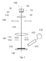
- Fig. 1 shows a schematic view of a focused ion beam device 100.
- the focused ion beam device 100 includes a charged particle gun 10 having a gun base 30, an emitter 20 and an extractor 40.
- the charged particle gun 10 is a gas field ion gun. Gas is supplied to the emitter 20 and an ion beam 110 is generated.
- the charged particle beam 110 passes through a condenser lens 140 and an aperture 180.
- a deflector unit 160 may include one or more deflectors 161 and 162 and directs the ion beam 110 to the specimen 120.
- the beam is focused on the specimen 120 on the specimen support 130 by objective lens 150.
- the detector 170 can include a scintillation element.
- An analyzer 175 processes the data received from the detector.
- the primary charged particle beam 110 is decelerated by an appropriate potential of the specimen and the secondary and/or backscattered charged particles are accelerated away from the specimen 120 towards the detection unit.
- the emitter 20 includes an emitter base tip and an emitter supertip.
- Fig. 2a shows a detailed top view of the construction of the emitter 20.
- the ion beam is emitted from the emitter supertip 22.
- the emitter base tip 21 includes a material that is different from the material of the supertip 22.
- the supertip 22 has one single atom 25 at its end.
- the base tip 21 can be a single crystal base tip.
- the single atom tip 22 provides at its top only one atom 25.
- the number of atoms in the adjacent layers of the single atom depends on the production process and the production conditions of the emitter tip.
- the supertip is produced by a coating of the base tip.
- the base tip can be a single crystal metal base tip.
- a thin tungsten single crystal tip can be coated with a palladium layer that has a thickness of about one, two or more palladium atom layers.
- the base tip may include materials like tungsten, tantalum, rhenium, molybdenum, niobium, and more refractory metals.
- the supertip may contain materials including platinum, rhodium, iridium and palladium.
- the coating of the base tip has a thickness of typically one, five or more atoms, more typically from one to three atoms.
- the supertip 22 is made of a material different from the material of the base tip 21. Accordingly, some layers being located under the single atom 25 of the coating of the supertip may contain one or more atoms from the material of the base tip 21.
- the supertip 22 is made of platinum and the base tip 21 is made of tungsten .
- some layers contain only platinum atoms, whereas some layers being located under the platinum layers may include tungsten atoms, too, due to the thickness of the platinum coating on the tungsten base tip.
- the different layers may contain only one type of atom, i.e. either only tungsten or only platinum.
- Fig. 2b the emission pattern of a particle beam device as known in the prior art is shown.
- the emitter tip in the prior art sources has, for instance, three or more atoms.
- Fig. 2b shows an emission pattern coming from a particle device with an emitter having three atoms at its tip, known as a trimer.
- the trimer emits charged particles in three separate beams. Only one of these three beams is used in order to limit aberrations of the lenses.
- the three beams coming from the trimer emitter tip "compete" for the gas supplied to the emitter tip. Every small disturbance of the system changes the ratio between the currents in the beam and accordingly the probe current.
- adsorbents next to the tip can start charged particle emission due to a local gas field enhancement. This reduces the gas transport to the trimer tip and consequently reduces the emission current.
- residual gases cause changes in the geometry of the tip shank, which influences field strength at the end of the tip and which results in emission current and consequently in probe current changes.
- the presented measurement device for CD and DR applications can overcome these limitations by building up a supertip on a single crystal base tip.
- a stable charged particle source with a one-atom tip can be provided which avoids the disadvantages of the trimer configuration mentioned above.
- Fig. 2c the emission pattern of a measurement device according to embodiments described herein is shown.
- the base tip can be a single crystal base tip.
- a single crystal does not have grain boundaries. This can be beneficial with regard to mechanical and electrical properties of the base tip, such as thermal conductivity, creeping, precipitation, and corrosion.
- the production of the single-atom tip is simplified and its functionality improved.
- the stability of the single-atom supertip and the stability of the ion beam generation are increased by the construction according to embodiments described herein.
- the gas field ion source includes an emitter tip, an electrode and a single emission centre.
- the emitter tip is made of an emitter base tip and a supertip.
- the material of the base tip is different from the material of the supertip.
- a voltage is supplied between the single emission centre of the supertip and the electrode.
- a gas is supplied to the emitter tip and the emitter tip surrounding region. Accordingly, an ion beam is generated coming from the single emission centre and including ions of the operation gas.
- only one stable ion beam is generated and directed to the sample.
- a specimen is analyzed with the ion beam and the structures of the specimen are classified by an analyzer.
- a controller can utilize the output of the analyzer. Thereby, the controller may act on the focused ion beam device or may feed forward or feed back the CD or DR information to other apparatus, which are provided in an in-line system, into which the focused ion beam is integrated.
- the focused ion beam device can be integrated in a semiconductor manufacturing system, such that an in-line focused ion beam device is provided.
- CD-measurements or DR-measurements can be provided, which can be used for feed back or feed forward of the analysis of the specimen.
- the single emission centre is provided by a single-atom supertip.
- the base tip is a single-crystal base tip.
- the base tip and/or the supertip are made of metal.
- the operation gas is helium, hydrogen, neon or the like.
- a controller may also control, among other things, the probe current.
- the controlling of the probe current may include a probe current measurement that can be accomplished by means for measuring the probe current like a Faraday cup, a biased Faraday cup, an electrode, a biased electrode, an inductive measurement unit, a scintillation detector, a combination thereof, or the like.
- the probe current measurement device generates a signal to trigger compensation actions to assure a stable probe current impinging on the sample and a proper function of the ion beam device.
- the sample charge is controlled.
- the charge control includes sample charge measurement.
- a retarding field configuration can be arranged to measure the sample charge.
- the measurement signal is used to calculate and cause countermeasures if necessary.
- the method includes a control loop to control the probe current and the countermeasures. Also, a control loop for the sample charge control is provided.
- a focused ion beam device with the probe current control is provided.
- a focused ion beam device with a probe current control can detect probe current changes and/or can initiate probe current stabilization measures for high precision measurement tools, like CD and DR.
- the spot size of the ion beam can be in a range by 0.1 nm
- the focused ion beam device requires a current stability which can be improved by the control of the probe current. This is even more desirable as the probe stability affects the measurement and imaging accuracy.
- Fig. 3a shows a schematic view of a focused ion beam device 100 with a probe current control and an analyzer 175 according to some embodiments described herein.
- An ion beam 110 is generated in a gas field ion source (not shown) including an emitter.
- the emitter is composed of an emitter base tip and an emitter supertip.
- Gas is supplied to the emitter region surrounding the emitter.
- the gas can be helium, hydrogen, argon, neon or the like.
- An extraction voltage is supplied to the emitter and causes the emitter to emit an ion beam including ions of the gas present in the emitter region.
- the ion beam 110 passes a condenser lens 140 that reduces the divergence or focuses the ion beam 110 coming from the ion beam source. Further, an aperture 180, where a portion of the ion beam 110 is blocked in order to shape the ion beam 110, is provided. According to embodiments described herein, the beam further passes an objective lens 150 before being deflected by a scan deflector 160.
- the scan deflector scans the ion beam 110 over the area of the specimen 120 that has to be inspected, measured, analyzed, manipulated, or the like.
- the specimen 120 is located on a specimen stage 130 that is controlled by the specimen stage control 135. Therefore, the sample stage 130 can be moved for having the scan area in the desired image region.
- the focused ion beam device 100 includes further beam optic elements, which can be one or more elements selected from the group consisting of: scanning deflectors, stigmators, focus adjustment units or focusing units for adjusting the focus of the ion beam, alignment deflectors, condenser lenses, accelerating electrodes or tubes for providing a beam boost potential (e.g., an increased potential in the column), or the like.
- beam optic elements can be one or more elements selected from the group consisting of: scanning deflectors, stigmators, focus adjustment units or focusing units for adjusting the focus of the ion beam, alignment deflectors, condenser lenses, accelerating electrodes or tubes for providing a beam boost potential (e.g., an increased potential in the column), or the like.
- the ion beam 110 impinges on the specimen 120. From the specimen, secondary and/or backscattered particles are released.
- the secondary and/or backscattered particles which are hereinafter referred to as secondary particles travel to the detector 170.
- the detector 170 generates a signal on impingement of the secondary particles, which is used for image generation during operation of the focused ion beam device.
- the detector 170 includes a scintillator.
- the detector 170 passes the signal and the information of the specimen to an analyzer 175.
- the analyzer is able to analyze and classify the structures present on the specimen. For instance, the analyzer can identify shapes such as circles, paths, trunks or the like, but also different materials being present on the specimen. Further, according to embodiments which can be combined with other embodiments described herein, the analyzer may detect exact dimensional values of the surface of the specimen, such as values for height, angle and dimensions of the structures of the specimen.
- the analyzer is a computer with hardware- and software components, allowing the execution of the above mentioned identification automatically.
- the control of the probe current includes the measurement of the probe current with a beam current measurement device.
- the beam current measurement device is part of the focused ion beam device including the gas field ion source-column and a sample chamber with the sample and a sample stage.
- the current measurement device can be part of the column, in order to allow monitoring current changes frequently. This has the benefit that no time consuming sample stage movements are required.
- some embodiments described herein include optionally a beam current probe measurement during line or image fly back time and/or during stage movement from one measurement area on the specimen to another specimen area on the specimen.
- the current changes can be controlled on request.
- the signal of the measured probe current is used to trigger counter measures to influence and correct the probe current.
- the countermeasures are carried out if it is indicated by the signal.
- the probe current can be measured continuously during the operation of the focused ion beam device.
- the countermeasure can also be applied continuously and only the amount of the countermeasure is amended according to the measured signal.
- the current measurement device can be a Faraday cup or another ion beam sensitive device.
- Fig. 3a an ion beam sensitive device 190 in the form of a Faraday cup is shown.
- the ion beam sensitive device is located on the sample stage and provides a current signal 195.
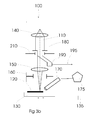
- Fig. 3b shows an ion beam sensitive device 190 in the form of a Faraday cup located within the beam column.
- the beam measurement device 190 is located behind the beam limiting aperture 180 to measure the probe current that in fact reaches the sample.
- a deflector 210 directs the ion beam 110 towards the ion beam sensitive device 190 that generates a current signal 195.
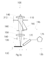
- Fig. 3c shows yet another embodiment described herein, where the ion beam sensitive device is located before the aperture 180.
- the beam current can be measured before reaching the aperture 180 in case the correlation between the current at this position and the final probe current is sufficient for the probe current control.
- a deflector 210 directs the ion beam 110 to the beam sensitive measurement device.
- a current signal 195 is generated by the measurement device 190.
- measuring a probe current according to any of the described measurement procedures, before a beam limiting element increases the signal to be measured.
- the final current on the specimen might then be calculated based on a calibration or a calculation.
- the deflector 210 can be an electrostatic deflector.
- the deflector is combined with a beam blanker.
- the beam blanker may be used as a deflector for current measurement.
- the beam blanker clears the beam, whenever a sample signal is not required.
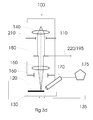
- Fig 3d shows yet another embodiment of the focused ion beam device.
- the beam limiting aperture 180 is suitable or adapted for accepting the measurement device.
- the aperture 180 can be the beam measurement device and can provide a current signal 195.
- the emission current supplied to the emitter tip can be measured in the voltage supply for the emitter tip of the GFIS, e.g., a HV supply for the GFIS, and can be used as a control signal.
- a beam current measurement assembly can include a beam modulation unit for repeatedly changing the current of the charged particle beam for providing a modulated charged particle beam, and a measurement unit adapted for measuring an inductive signal generated by the repeatedly changing charged particle beam current.
- the measuring unit can be provided by a conductive loop in the vicinity or typically around the charged particle beam. Basically such an arrangement might be interpreted as a transformer in which the modulated charged particle beam is the primary coil (having one winding) and having a secondary coil or a magnetic circuit around the charged particle beam.
- the probe current measurement requires a stage controller in case that the measurement device is on the stage as shown in Fig. 3a .
- An actuator may also be provided to move an in-column current measurement unit in the event an in-column measurement device is moved mechanically.
- a deflection device for instance an electrostatic deflector, is provided which directs the beam to the in-column measurement device or the measurement device on the specimen stage.
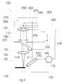
- Fig. 4 several control mechanisms and a control unit is shown to control the beam current.
- the beam current is measured as described above.
- a control unit 240 is provided to influence the beam current.
- the control unit 240 interacts with the deflector control 230 and the control loop 300.
- the control unit includes a calculation unit.
- the calculation unit calculates the necessity of countermeasures when the probe current changes. This may be done by comparing the probe current to threshold values according to look-up tables or the like.
- control unit 240 can automatically execute the controlling.
- control unit may also be able to control the further steps of the operation.
- results from the analyzer can be used for adapting operation of the focused ion beam device.
- the controller may alternatively or additionally be connected to other devices in an in-line semiconductor manufacturing tool. Thereby, the information from the analyzer can be used by the controller to provide desired information to other devices.
- the controller may calculate the necessary measures according to the output of the analyzer 175.
- the output of the analyzer may include information about the correctness of the structure on the specimen.
- control unit 240 can control the sort of action the control loop 300 should fulfill. According to another embodiment, the control unit 240 can control the amount of action of the control loop 300. According to yet another embodiment, the control unit 240 initiates the control loop 300 without limiting the control loop action in any way. According to some embodiments which can be combined with other embodiments described herein, the control unit may also initiate specimen change if necessary or direct the inspected specimen to another device being able to modify the specimen in case that the analyzer gives information, which indicates that a modification of the specimen should be conducted. Alternatively, the specimen does not have to change the device for being structured but may also be structured in the same device.
- the control loop 300 can automatically control changing of the emission current. According to some embodiments that can be combined with other embodiments described herein, the control loop receives instructions from the control unit 240. These instructions may include the necessity of countermeasures, the sort of countermeasures or the amount of countermeasures.
- the control loop can control one or more of the group including the gas flow 250, the temperature of the emitter 260, the suppressor voltage 275, the extractor voltage 285, and the condenser excitation 290.
- the amount of gas is controlled that is condensed on the emitter and the emitter tip.
- the suppressor electrode 270 allows controlling field extraction strength indirectly and allows therefore controlling the emission current that correlates with the probe current.
- a suppressor 270 in the form of an additional electrode is provided next to the gas field ion source.
- Another possibility to control the emission current is changing the extraction voltage.
- the condenser lens excitation can be controlled. Thereby, the probe current density on the aperture 180 is influenced.
- the detection channel can be calibrated to compensate the detector signal according to the probe current change to achieve improved measurement accuracy.
- the detection channel in this context should be understood as image generation measurement signals based on detection of secondary particles from the specimen or the like.
- sample charge measurement may be provided.
- sample charge control may be provided.
- sample dosage control may be provided.
- ions impinge on the sample.
- the sample will be charged positively due to the ion impingement. This charging can influence the imaging of sample details and their quantitative dimension measurement in a negative manner. Typically, the sub-nanometer resolution can no longer be ensured. Therefore, the measurement of the surface charge of the sample during imaging, measuring or processing is provided.
- the focused ion beam device can include a sample charge control.
- the sample charge control contains a charge measurement device.
- the charge measurement device includes an energy sensitive detector, such as a spectrometer. Providing a spectrometer within the detection path allows surface voltage measurement of the sample.
- detection path in this context should be understood as the path between the sample surface and a detection arrangement, for instance a detector.
- the received charge measurement can be used to trigger compensation measures.
- a beam blanker that blanks the ion beam when a sample signal is not required, e.g., during line fly back, image fly back or an idle period of the system. This reduces the sample dosage and therefore sample charging. By reducing the sample charge, the measurement and imaging accuracy is improved.
- the beam blanker can be used and combined as a deflection device for current measurements described above. Thereby, it might be possible that during beam blanking, the probe current is measured and the current changes are compensated.
- a retarding field configuration is used to measure the sample charge and create a signal according to the sample charge.
- a retarding field configuration is for instance shown in Fig. 5a .
- the retarding field configuration is located within the signal detection path.
- a retarding field configuration can include a retarding field detector and an electrode.
- the electrode can be an aperture or a grid or the like located between the sample surface and the detector. In case the sample is charged positively, the electrode is biased negatively and can act as a filter for secondary particles. Secondary particles with energy below a certain threshold value cannot pass the electrode. The remaining particles with energy above the threshold value can pass the filter electrode and are detected by the detector.
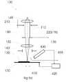
- a post-lens arrangement of a retarding field configuration is shown, that means, the retarding field configuration or only the filter electrode is located beneath the objective lens.
- a filter electrode 430 is placed between sample 120 and detector 170.
- the electrode control 435 controls the energy supplied to the electrode to maintain a negative charging that corresponds to a predetermined threshold value for the energy of the secondary particles that should be filtered.
- a sample charge device 410 is provided. The secondary particles travel from the sample to the electrode and pass the filter electrode 430 if their energy is high enough.
- the detector 170 detects the filtered particles and generates a signal. The signal can be used to determine the surface voltage, e.g. by look-up tables or by using feedback loops keeping the detector signal constant.
- This signal is forwarded to the control unit 420 that calculates the necessary compensation measure and controls the sample charge device 410.
- the sample charge device provides energy to the sample according to the instruction received from the control unit 420. Therefore, the sample charge resulting from the impingement of the ions can be compensated.
- the configuration of Fig. 5a and 5b can be combined with embodiments described herein, but for the sake of simplicity, for instance the analyzer and the control unit is not shown in these figures.
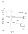
- Fig. 5b another embodiment of the focused ion beam device with a sample charge control is shown.
- the retarding field configuration is arranged in a pre-lens arrangement.
- the term "pre-lens arrangement" in this context should be understood as an arrangement that is located above the objective lens 150.
- the filter electrode 430 is charged negatively in order to filter secondary particles having certain energy.
- the charging of the filter electrode is controlled by an electrode control 435.
- a detector 440 is provided to detect the filtered secondary particles coming from the sample and filtered by the electrode 430.
- the retarding detector can be for instance ring-shaped or segmented.
- Fig. 5a an off-axis detector is shown, that means, the detector is arranged next to the optical axis, i.e., essentially the ion beam axis.
- Fig. 5b shows an on-axis configuration. Being arranged in an on-axis configuration means that the detector is orientated on the axis of the ion beam.
- the term "off-axis arrangement" should be understood as an arrangement being beside the beam axis 50.
- the detector 170 can be arranged in an on-axis arrangement.
- on-axis arrangement means, that the detector is located on the axis 50.
- the filter electrode may also have different shapes depending on whether an off-axis or an on-axis configuration is chosen.
- the filter electrode 430 can be located between the sample 120 and the detector and does not have to be directly in front of the detector. Also, configurations placing the electrode above the sample surface, inside the objective lens or between objective lens and detector are in the scope of the invention.
- Fig. 5b further shows a flood gun 460 to control and compensate the sample charge.
- the control unit 450 receives a signal from the detector containing information about the sample charge.
- the control unit 450 can calculate necessary countermeasures to keep the sample charge at a desired level and forward a signal to the flood gun 460.
- the flood gun 460 can operate in the amount necessary to compensate the sample charge.
- a method of operating an ion beam device is provided.
- a voltage is supplied between an emitter and an electrode.
- the emitter includes an emitter base tip and an emitter supertip.
- a gas is supplied in the emitter region and the emitter emits ions of that operation gas.
- the resulting ion beam with a beam current is directed towards a sample in order to inspect or process the sample.
- the beam current is controlled by measuring the beam current with a beam current device.
- the probe current measurement generates a signal that can be used to trigger a compensation measure.
- a varying probe current is not desirable due to varying beam stability and therefore varying operation quality, it is desirable to keep the probe current at a certain level. This level may be predetermined or dependent on the operation.
- the emission current can be changed by changing the extraction voltage of the emitter.
- the probe current depends directly on the emission current.
- an additional electrode can be provided acting as a suppressor to control the beam current.
- the suppressor can influence the field extraction strength and therefore the emission current.
- Another possibility arises from controlling the gas flow and/or the emitter temperature to affect the amount of gas condensation on the emitter.
- the probe current density can be changed by controlling the excitation of the condenser lens. According to some embodiments, these possibilities can be combined in any manner. According to other embodiments described herein, the possibilities can be used individually.
- the probe current is controlled typically on a basis of 10 minutes or less, typically quasi continuously or continuously.
- the probe current can be measured and controlled continuously. Therefore, compensation measures as described above can be initiated. Thereby, according to different options, compensation can start directly if the beam current changes. According to an alternative modification, the compensation may be started in the near future after the probe current changed, e.g. after the present specimen has been moved out of the ion beam system.
- the method of operating a focused ion beam device further includes measuring and controlling the sample charge.
- a voltage is supplied between an emitter and an electrode of the focused ion beam device and a gas is supplied to the region surrounding the emitter tip, the emitter tip region. Ions of the gas are emitted and the sample charge is measured and controlled.
- the sample charge is measured during operation of the focused ion beam device. According to some embodiments, the sample charge is measured and controlled on a basis of 10 minutes or less, typically quasi continuously or continuously.
- the method further includes detecting a signal that is generated by the impingement of charged particles on the sample.
- a detector detects secondary particles that are caused by the impingement of the charged particle beam. These particles are emitted from the sample and travel to the detector.
- the signal of the detector can be used to trigger an event or to generate an image of the sample.
- a retarding field is implemented to measure the sample charge.
- the retarding field is located between the sample and the detector, whereby the detector can be arranged in a post-lens or a pre-lens configuration.
- the detector may be in an on- or an off-axis arrangement.
- the retarding field configuration can be a detector and a filter electrode.
- a control voltage can be supplied to the sample in order to compensate the sample charge generated by the charged particles.
- the control voltage may be provided by a conductive sample carrier, a flood gun or the like. The voltage is supplied for a certain time period. In this time, the sample charge measurement is continued and the values are compared with the desired threshold values. If the measured value of the sample charge is equal to or less than the threshold value, the control voltage is stopped.
- control voltage is supplied to the sample carrier continuously and the amount of the control voltage is changed according to the trigger signal that is based on the measured sample charge. Therefore, the sample charge is constant or at a defined level during operation of the focused ion beam device.
- a focused ion beam device including a gas field ion source with an emitter emitting an ion beam including ions of gas, an ion beam column and a sample charge control including a sample charge measurement unit.
- a focused ion beam device wherein the emitter may include an emitter base tip and an emitter supertip.
- the focused ion beam device with sample charge control may include a spectrometer for sample charge control.
- the focused ion beam device may include a retarding field configuration for sample charge control.
- the focused ion beam device may contain a detector for measuring the sample charge.
- the focused ion beam device may include a sample charge measurement unit and a detector for controlling the sample charge.
- a method of operating an ion beam device having an ion beam column and a gas field ion source with an emitter tip in an emitter tip region includes applying a voltage between an emitter and an electrode, applying a gas to the emitter tip region, emitting ions of a gas from the emitter, and measuring and controlling a sample charge.
- the method may include measuring and controlling the sample charge during operation of the ion beam device.
- the sample charge may be measured and controlled when changes to a threshold value have reached a predetermined limit, prior to the CD or DR imaging or before a certain number n of measurements has been conducted.
- a signal may be detected that is generated by the impingement of the ion beam on a sample by a detector.
- the measuring of the sample charge may include the implementation of a retarding field configuration between the sample and the detector.
- compensation measures can be triggered based on the measurement of the sample charge.
- a control voltage may be supplied to the sample after measuring the sample charge.
- a control voltage may be supplied to a sample carrier after measuring the sample charge.
- the method of operating an ion beam device includes controlling the sample charge by a control loop.
Landscapes
- Chemical & Material Sciences (AREA)
- Analytical Chemistry (AREA)
- Engineering & Computer Science (AREA)
- Combustion & Propulsion (AREA)
- Electron Sources, Ion Sources (AREA)
Priority Applications (2)
| Application Number | Priority Date | Filing Date | Title |
|---|---|---|---|
| EP08156665A EP2124245A1 (de) | 2008-05-21 | 2008-05-21 | Hochpräzises Messinstrument |
| US12/133,298 US8785849B2 (en) | 2008-05-21 | 2008-06-04 | Ultra high precision measurement tool |
Applications Claiming Priority (1)
| Application Number | Priority Date | Filing Date | Title |
|---|---|---|---|
| EP08156665A EP2124245A1 (de) | 2008-05-21 | 2008-05-21 | Hochpräzises Messinstrument |
Publications (1)
| Publication Number | Publication Date |
|---|---|
| EP2124245A1 true EP2124245A1 (de) | 2009-11-25 |
Family
ID=39739959
Family Applications (1)
| Application Number | Title | Priority Date | Filing Date |
|---|---|---|---|
| EP08156665A Withdrawn EP2124245A1 (de) | 2008-05-21 | 2008-05-21 | Hochpräzises Messinstrument |
Country Status (2)
| Country | Link |
|---|---|
| US (1) | US8785849B2 (de) |
| EP (1) | EP2124245A1 (de) |
Cited By (2)
| Publication number | Priority date | Publication date | Assignee | Title |
|---|---|---|---|---|
| CN109225301A (zh) * | 2018-10-16 | 2019-01-18 | 中国科学技术大学先进技术研究院 | 一种Ir/Co0.8Fe0.2Se2-NF单原子催化剂及其制备方法、应用 |
| DE102017120408A1 (de) * | 2017-09-05 | 2019-03-07 | scia Systems GmbH | Verfahren und Anordnung zum Ermitteln eines elektrischen Potentials und zum Ermitteln einer Verteilungsdichtefunktion eines Stromes von einem Strahl von Teilchen |
Families Citing this family (4)
| Publication number | Priority date | Publication date | Assignee | Title |
|---|---|---|---|---|
| EP2124244B1 (de) * | 2008-05-21 | 2011-08-03 | ICT, Integrated Circuit Testing Gesellschaft für Halbleiterprüftechnik mbH | Hochpräzises Messinstrument mit Steuerkreis |
| US8847173B2 (en) * | 2010-08-06 | 2014-09-30 | Hitachi High-Technologies Corporation | Gas field ion source and method for using same, ion beam device, and emitter tip and method for manufacturing same |
| JP6894486B2 (ja) * | 2016-07-05 | 2021-06-30 | 株式会社日立ハイテクサイエンス | イオンビーム装置 |
| EP3945539B1 (de) | 2020-07-31 | 2023-06-07 | Centre National de la Recherche Scientifique | Gasionenkanone |
Citations (3)
| Publication number | Priority date | Publication date | Assignee | Title |
|---|---|---|---|---|
| JPS61135035A (ja) * | 1984-12-05 | 1986-06-23 | Toshiba Corp | 電子ビ−ムテスタ用表面電位測定装置 |
| US20050092922A1 (en) * | 2000-07-18 | 2005-05-05 | Hiroyuki Muto | Ion beam apparatus and sample processing method |
| US20070138388A1 (en) * | 2003-10-16 | 2007-06-21 | Ward Billy W | Ion sources, systems and methods |
Family Cites Families (6)
| Publication number | Priority date | Publication date | Assignee | Title |
|---|---|---|---|---|
| US6452174B1 (en) * | 1999-12-13 | 2002-09-17 | Mitsubishi Denki Kabushiki Kaisha | Charged particle beam apparatus and method of controlling same |
| JP2002298132A (ja) * | 2001-04-02 | 2002-10-11 | Fuji Mach Mfg Co Ltd | 撮像システム,撮像システム制御プログラムおよび電気部品装着システム |
| US6727501B1 (en) * | 2001-09-27 | 2004-04-27 | Kla-Tencor Corporation | Method for detecting over-etch defects |
| KR20060043141A (ko) * | 2004-02-23 | 2006-05-15 | 지벡스 코포레이션 | 대전 입자 빔 장치 프로브 조작기 |
| US7859279B2 (en) * | 2006-11-01 | 2010-12-28 | Tokyo Electron Limited | Charge eliminating apparatus and method, and program storage medium |
| JP2008209291A (ja) * | 2007-02-27 | 2008-09-11 | Hitachi Ltd | Nmr装置 |
-
2008
- 2008-05-21 EP EP08156665A patent/EP2124245A1/de not_active Withdrawn
- 2008-06-04 US US12/133,298 patent/US8785849B2/en active Active
Patent Citations (3)
| Publication number | Priority date | Publication date | Assignee | Title |
|---|---|---|---|---|
| JPS61135035A (ja) * | 1984-12-05 | 1986-06-23 | Toshiba Corp | 電子ビ−ムテスタ用表面電位測定装置 |
| US20050092922A1 (en) * | 2000-07-18 | 2005-05-05 | Hiroyuki Muto | Ion beam apparatus and sample processing method |
| US20070138388A1 (en) * | 2003-10-16 | 2007-06-21 | Ward Billy W | Ion sources, systems and methods |
Non-Patent Citations (3)
| Title |
|---|
| HONG-SHI KUO ET AL: "Noble Metal/W(111) Single-Atom Tips and Their Field Electron and Ion Emission Characteristics", JAPANESE JOURNAL OF APPLIED PHYSICS, JAPAN SOCIETY OF APPLIED PHYSICS, TOKYO.; JP, vol. 45, no. 11, 8 November 2006 (2006-11-08), pages 8972 - 8983, XP007903666, ISSN: 0021-4922 * |
| KUO HONG-SHI ET AL: "Preparation and characterization of single-atom tips", NANO LETTERS, ACS, WASHINGTON, DC, US, vol. 4, no. 12, 1 December 2004 (2004-12-01), pages 2379 - 2382, XP002439176, ISSN: 1530-6984 * |
| TSU-YI FU ET AL: "Method of creating a Pd-covered single-atom sharp W pyramidal tip: Mechanism and energetics of its formation", PHYSICAL REVIEW. B, CONDENSED MATTER AND MATERIALS PHYSICS, AMERICAN INSTITUTE OF PHYSICS, WOODBURY, NY, US, vol. 64, no. 11, 15 September 2001 (2001-09-15), pages 113401/1 - 113401/4, XP002439177, ISSN: 1098-0121 * |
Cited By (4)
| Publication number | Priority date | Publication date | Assignee | Title |
|---|---|---|---|---|
| DE102017120408A1 (de) * | 2017-09-05 | 2019-03-07 | scia Systems GmbH | Verfahren und Anordnung zum Ermitteln eines elektrischen Potentials und zum Ermitteln einer Verteilungsdichtefunktion eines Stromes von einem Strahl von Teilchen |
| DE102017120408B4 (de) * | 2017-09-05 | 2020-11-19 | scia Systems GmbH | Verfahren und Anordnung zum Ermitteln eines elektrischen Potentials und zum Ermitteln einer Verteilungsdichtefunktion eines Stromes von einem Strahl von Teilchen |
| CN109225301A (zh) * | 2018-10-16 | 2019-01-18 | 中国科学技术大学先进技术研究院 | 一种Ir/Co0.8Fe0.2Se2-NF单原子催化剂及其制备方法、应用 |
| CN109225301B (zh) * | 2018-10-16 | 2021-04-23 | 中国科学技术大学先进技术研究院 | 一种Ir/Co0.8Fe0.2Se2-NF单原子催化剂及其制备方法、应用 |
Also Published As
| Publication number | Publication date |
|---|---|
| US20090289185A1 (en) | 2009-11-26 |
| US8785849B2 (en) | 2014-07-22 |
Similar Documents
| Publication | Publication Date | Title |
|---|---|---|
| US7851768B2 (en) | Ultra high precision measurement tool with control loop | |
| US10522327B2 (en) | Method of operating a charged particle beam specimen inspection system | |
| US11170970B2 (en) | Methods and devices for examining an electrically charged specimen surface | |
| CN110214361B (zh) | 用于检查样本的方法和带电粒子多束装置 | |
| US7067807B2 (en) | Charged particle beam column and method of its operation | |
| US9437395B2 (en) | Method and compound system for inspecting and reviewing defects | |
| JP2008176984A (ja) | イオンビーム加工装置 | |
| TWI912792B (zh) | 光罩或晶圓進行檢查、修復、或電路修補方法 | |
| US8785849B2 (en) | Ultra high precision measurement tool | |
| JP2009043936A (ja) | 電子顕微鏡 | |
| JP2015216086A (ja) | 荷電粒子線装置及び当該装置を用いる検査方法 | |
| EP2088614A1 (de) | Strahlstromkalibriersystem | |
| US9184024B2 (en) | Selectable coulomb aperture in E-beam system | |
| JP2007207688A (ja) | ミラー電子顕微鏡およびミラー電子顕微鏡を用いた検査装置 | |
| EP1760762B1 (de) | Vorrichtung und Verfahren zur Auswahl einer Emissionsfläche einer Emissionsstruktur | |
| EP2110844A1 (de) | Berührungslose Messung des Strahlstroms in einem geladenen Partikelstrahlsystem | |
| US6952105B2 (en) | Inspection method and apparatus for circuit pattern of resist material | |
| US7132301B1 (en) | Method and apparatus for reviewing voltage contrast defects in semiconductor wafers | |
| US20250132121A1 (en) | Method of operating a charged particle beam apparatus, and charged particle beam apparatus | |
| US7170068B2 (en) | Method and system for discharging a sample | |
| US7525091B2 (en) | Charged particle beam system and a method for inspecting a sample | |
| US20240006147A1 (en) | Flood column and charged particle apparatus | |
| JP2008076070A (ja) | 荷電粒子ビーム検査方法及び装置 |
Legal Events
| Date | Code | Title | Description |
|---|---|---|---|
| PUAI | Public reference made under article 153(3) epc to a published international application that has entered the european phase |
Free format text: ORIGINAL CODE: 0009012 |
|
| AK | Designated contracting states |
Kind code of ref document: A1 Designated state(s): AT BE BG CH CY CZ DE DK EE ES FI FR GB GR HR HU IE IS IT LI LT LU LV MC MT NL NO PL PT RO SE SI SK TR |
|
| AX | Request for extension of the european patent |
Extension state: AL BA MK RS |
|
| 17P | Request for examination filed |
Effective date: 20100428 |
|
| AKX | Designation fees paid |
Designated state(s): DE NL |
|
| 17Q | First examination report despatched |
Effective date: 20101019 |
|
| STAA | Information on the status of an ep patent application or granted ep patent |
Free format text: STATUS: THE APPLICATION IS DEEMED TO BE WITHDRAWN |
|
| 18D | Application deemed to be withdrawn |
Effective date: 20151201 |