EP2124253B1 - Hochfrequenzkapselung - Google Patents
Hochfrequenzkapselung Download PDFInfo
- Publication number
- EP2124253B1 EP2124253B1 EP08720878.1A EP08720878A EP2124253B1 EP 2124253 B1 EP2124253 B1 EP 2124253B1 EP 08720878 A EP08720878 A EP 08720878A EP 2124253 B1 EP2124253 B1 EP 2124253B1
- Authority
- EP
- European Patent Office
- Prior art keywords
- radio
- frequency
- signal
- conductor pad
- dielectric substrate
- Prior art date
- Legal status (The legal status is an assumption and is not a legal conclusion. Google has not performed a legal analysis and makes no representation as to the accuracy of the status listed.)
- Active
Links
Images



Classifications
-
- H—ELECTRICITY
- H10—SEMICONDUCTOR DEVICES; ELECTRIC SOLID-STATE DEVICES NOT OTHERWISE PROVIDED FOR
- H10W—GENERIC PACKAGES, INTERCONNECTIONS, CONNECTORS OR OTHER CONSTRUCTIONAL DETAILS OF DEVICES COVERED BY CLASS H10
- H10W76/00—Containers; Fillings or auxiliary members therefor; Seals
- H10W76/10—Containers or parts thereof
- H10W76/12—Containers or parts thereof characterised by their shape
- H10W76/13—Containers comprising a conductive base serving as an interconnection
-
- H—ELECTRICITY
- H01—ELECTRIC ELEMENTS
- H01P—WAVEGUIDES; RESONATORS, LINES, OR OTHER DEVICES OF THE WAVEGUIDE TYPE
- H01P1/00—Auxiliary devices
-
- H—ELECTRICITY
- H10—SEMICONDUCTOR DEVICES; ELECTRIC SOLID-STATE DEVICES NOT OTHERWISE PROVIDED FOR
- H10W—GENERIC PACKAGES, INTERCONNECTIONS, CONNECTORS OR OTHER CONSTRUCTIONAL DETAILS OF DEVICES COVERED BY CLASS H10
- H10W42/00—Arrangements for protection of devices
- H10W42/20—Arrangements for protection of devices protecting against electromagnetic or particle radiation, e.g. light, X-rays, gamma-rays or electrons
-
- H—ELECTRICITY
- H10—SEMICONDUCTOR DEVICES; ELECTRIC SOLID-STATE DEVICES NOT OTHERWISE PROVIDED FOR
- H10W—GENERIC PACKAGES, INTERCONNECTIONS, CONNECTORS OR OTHER CONSTRUCTIONAL DETAILS OF DEVICES COVERED BY CLASS H10
- H10W44/00—Electrical arrangements for controlling or matching impedance
- H10W44/20—Electrical arrangements for controlling or matching impedance at high-frequency [HF] or radio frequency [RF]
-
- H—ELECTRICITY
- H10—SEMICONDUCTOR DEVICES; ELECTRIC SOLID-STATE DEVICES NOT OTHERWISE PROVIDED FOR
- H10W—GENERIC PACKAGES, INTERCONNECTIONS, CONNECTORS OR OTHER CONSTRUCTIONAL DETAILS OF DEVICES COVERED BY CLASS H10
- H10W44/00—Electrical arrangements for controlling or matching impedance
- H10W44/20—Electrical arrangements for controlling or matching impedance at high-frequency [HF] or radio frequency [RF]
- H10W44/203—Electrical connections
- H10W44/206—Wires
-
- H—ELECTRICITY
- H10—SEMICONDUCTOR DEVICES; ELECTRIC SOLID-STATE DEVICES NOT OTHERWISE PROVIDED FOR
- H10W—GENERIC PACKAGES, INTERCONNECTIONS, CONNECTORS OR OTHER CONSTRUCTIONAL DETAILS OF DEVICES COVERED BY CLASS H10
- H10W44/00—Electrical arrangements for controlling or matching impedance
- H10W44/20—Electrical arrangements for controlling or matching impedance at high-frequency [HF] or radio frequency [RF]
- H10W44/203—Electrical connections
- H10W44/216—Waveguides, e.g. strip lines
-
- H—ELECTRICITY
- H10—SEMICONDUCTOR DEVICES; ELECTRIC SOLID-STATE DEVICES NOT OTHERWISE PROVIDED FOR
- H10W—GENERIC PACKAGES, INTERCONNECTIONS, CONNECTORS OR OTHER CONSTRUCTIONAL DETAILS OF DEVICES COVERED BY CLASS H10
- H10W70/00—Package substrates; Interposers; Redistribution layers [RDL]
- H10W70/60—Insulating or insulated package substrates; Interposers; Redistribution layers
- H10W70/62—Insulating or insulated package substrates; Interposers; Redistribution layers characterised by their interconnections
- H10W70/63—Vias, e.g. via plugs
-
- H—ELECTRICITY
- H10—SEMICONDUCTOR DEVICES; ELECTRIC SOLID-STATE DEVICES NOT OTHERWISE PROVIDED FOR
- H10W—GENERIC PACKAGES, INTERCONNECTIONS, CONNECTORS OR OTHER CONSTRUCTIONAL DETAILS OF DEVICES COVERED BY CLASS H10
- H10W70/00—Package substrates; Interposers; Redistribution layers [RDL]
- H10W70/60—Insulating or insulated package substrates; Interposers; Redistribution layers
- H10W70/67—Insulating or insulated package substrates; Interposers; Redistribution layers characterised by their insulating layers or insulating parts
- H10W70/68—Shapes or dispositions thereof
- H10W70/682—Shapes or dispositions thereof comprising holes having chips therein
-
- H—ELECTRICITY
- H10—SEMICONDUCTOR DEVICES; ELECTRIC SOLID-STATE DEVICES NOT OTHERWISE PROVIDED FOR
- H10W—GENERIC PACKAGES, INTERCONNECTIONS, CONNECTORS OR OTHER CONSTRUCTIONAL DETAILS OF DEVICES COVERED BY CLASS H10
- H10W70/00—Package substrates; Interposers; Redistribution layers [RDL]
- H10W70/60—Insulating or insulated package substrates; Interposers; Redistribution layers
- H10W70/67—Insulating or insulated package substrates; Interposers; Redistribution layers characterised by their insulating layers or insulating parts
- H10W70/68—Shapes or dispositions thereof
- H10W70/685—Shapes or dispositions thereof comprising multiple insulating layers
-
- H—ELECTRICITY
- H10—SEMICONDUCTOR DEVICES; ELECTRIC SOLID-STATE DEVICES NOT OTHERWISE PROVIDED FOR
- H10W—GENERIC PACKAGES, INTERCONNECTIONS, CONNECTORS OR OTHER CONSTRUCTIONAL DETAILS OF DEVICES COVERED BY CLASS H10
- H10W72/00—Interconnections or connectors in packages
- H10W72/071—Connecting or disconnecting
- H10W72/075—Connecting or disconnecting of bond wires
- H10W72/07551—Connecting or disconnecting of bond wires characterised by changes in properties of the bond wires during the connecting
- H10W72/07552—Connecting or disconnecting of bond wires characterised by changes in properties of the bond wires during the connecting changes in structures or sizes
-
- H—ELECTRICITY
- H10—SEMICONDUCTOR DEVICES; ELECTRIC SOLID-STATE DEVICES NOT OTHERWISE PROVIDED FOR
- H10W—GENERIC PACKAGES, INTERCONNECTIONS, CONNECTORS OR OTHER CONSTRUCTIONAL DETAILS OF DEVICES COVERED BY CLASS H10
- H10W72/00—Interconnections or connectors in packages
- H10W72/50—Bond wires
-
- H—ELECTRICITY
- H10—SEMICONDUCTOR DEVICES; ELECTRIC SOLID-STATE DEVICES NOT OTHERWISE PROVIDED FOR
- H10W—GENERIC PACKAGES, INTERCONNECTIONS, CONNECTORS OR OTHER CONSTRUCTIONAL DETAILS OF DEVICES COVERED BY CLASS H10
- H10W72/00—Interconnections or connectors in packages
- H10W72/50—Bond wires
- H10W72/521—Structures or relative sizes of bond wires
-
- H—ELECTRICITY
- H10—SEMICONDUCTOR DEVICES; ELECTRIC SOLID-STATE DEVICES NOT OTHERWISE PROVIDED FOR
- H10W—GENERIC PACKAGES, INTERCONNECTIONS, CONNECTORS OR OTHER CONSTRUCTIONAL DETAILS OF DEVICES COVERED BY CLASS H10
- H10W72/00—Interconnections or connectors in packages
- H10W72/50—Bond wires
- H10W72/551—Materials of bond wires
- H10W72/552—Materials of bond wires comprising metals or metalloids, e.g. silver
- H10W72/5522—Materials of bond wires comprising metals or metalloids, e.g. silver comprising gold [Au]
-
- H—ELECTRICITY
- H10—SEMICONDUCTOR DEVICES; ELECTRIC SOLID-STATE DEVICES NOT OTHERWISE PROVIDED FOR
- H10W—GENERIC PACKAGES, INTERCONNECTIONS, CONNECTORS OR OTHER CONSTRUCTIONAL DETAILS OF DEVICES COVERED BY CLASS H10
- H10W72/00—Interconnections or connectors in packages
- H10W72/50—Bond wires
- H10W72/59—Bond pads specially adapted therefor
-
- H—ELECTRICITY
- H10—SEMICONDUCTOR DEVICES; ELECTRIC SOLID-STATE DEVICES NOT OTHERWISE PROVIDED FOR
- H10W—GENERIC PACKAGES, INTERCONNECTIONS, CONNECTORS OR OTHER CONSTRUCTIONAL DETAILS OF DEVICES COVERED BY CLASS H10
- H10W90/00—Package configurations
- H10W90/701—Package configurations characterised by the relative positions of pads or connectors relative to package parts
- H10W90/751—Package configurations characterised by the relative positions of pads or connectors relative to package parts of bond wires
- H10W90/754—Package configurations characterised by the relative positions of pads or connectors relative to package parts of bond wires between a chip and a stacked insulating package substrate, interposer or RDL
Definitions
- the present invention relates to a radio-frequency package equipped with a radio-frequency device that operates in a radio-frequency band such as a microwave band or a millimeter-wave band, and more particularly, to a radio-frequency package capable of suppressing a leakage (spurious) of a radio-frequency signal from a radio-frequency device to the outside.
- a radio-frequency band such as a microwave band or a millimeter-wave band
- An automotive millimeter-wave radar that detects a distance and a relative speed to a vehicle in front by the use of an electromagnetic wave in a millimeter-wave band is applied to a cruise control and safety measures, for example, for reducing damage to a driver in case a vehicle collision is inevitable.
- a method of multiplying a low frequency is mostly employed.
- lots of frequency components exist in a module, so that it is extremely difficult to meet overseas EMI standards (such as the FCC).
- a radar module In an automotive millimeter-wave radar, a radar module generally includes a radio-frequency package equipped with a radio-frequency device for a radar device, a control/interface substrate that supplies a bias signal and a control signal to the radio-frequency package, a waveguide plate, and the like. To meet the EMI standards, in conventional technologies, the entire radar module is generally covered with a metal cover.
- an integrated-circuit component for radio-frequency signal and a dielectric substrate are mounted on a metallic base member, and a microstrip line is formed on the dielectric substrate.
- the base member on which the integrated-circuit component for radio-frequency signal and the dielectric substrate are mounted is covered with a metallic frame member and a metallic cover member.
- the integrated-circuit component for radio-frequency signal mounted on the base member is supplied with a bias via a bias terminal.
- a further example for a radio-frequency package is disclosed in EP 1 729 340 A1 .
- Patent document 1 Japanese Patent Application Laid-open No. 2000-31712
- a radio-frequency package is enclosed by the metal base, the metallic frame member, and the metallic cover member, so that leakage of a radio-frequency component to the outside is suppressed to some degree.
- any countermeasures against a radio-frequency component leaking through the bias terminal are not taken. Therefore, there is a problem that the radio-frequency component as a spurious that is electromagnetically coupled to the bias terminal in a radio-frequency package is radiated to the outside through the bias terminal.
- a radio-frequency device is mounted on a surface layer of a multilayer dielectric, and a portion of the surface layer of the multilayer dielectric substrate and the radio-frequency device are covered with an electromagnetic shield member.
- an external terminal arranged outside the electromagnetic shield member is connected to an internal terminal inside the electromagnetic shield member through a signal via-hole, an inner-layer signal line, and a signal via-hole in the multilayer dielectric substrate, and the internal terminal is further electrically-connected to the radio-frequency device via a wire. Therefore, the conventional radio-frequency package has a problem that spurious emission propagating through an internal space formed by the electromagnetic shield member is coupled to the wire, and radiated to the outside through a bias line provided in an inner layer of the dielectric substrate.
- the present invention has been made in view of the above problems, and an object of the present invention is to provide a radio-frequency package with a high radio-frequency shielding performance at low cost by reducing a level of spurious coupled to a wire and thereby suppressing a level of spurious emission to the outside within the radio-frequency package.
- a leading-end open line having a length equivalent to substantially a quarter of a wavelength of a radio-frequency signal (spurious) used in a radio-frequency device is provided to an internal conductor pad for bias/control signal.
- the spurious coupled to a wire is reflected by the leading-end open line provided to the internal conductor pad. Therefore, it is possible to reduce a level of spurious coupled to the wire, and thus it is possible to reduce a level of spurious leaking to the outside. Consequently, it is possible to suppress leakage of spurious to outside a radio-frequency package reliably. In this manner, within the radio-frequency package, leakage of a radio-frequency component to outside the radio-frequency package can be suppressed, reducing a production cost.
- Fig. 1 is a cross-sectional view illustrating a configuration of a transmitter/receiver module 10 in which a radio-frequency package 1 is mounted.
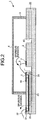
- Fig. 2 is a cross-sectional view illustrating a configuration of the radio-frequency package 1.
- the transmitter/receiver module 10 is applied, for example, to an FM-CW radar having a function of detecting a distance and a relative speed to a target (such as a vehicle) in front by the use of an electromagnetic wave in a millimeter-wave band.
- the FM-CW radar irradiates the target with a frequency-modulated radio-frequency signal (a transmitted signal), detects a difference in frequency between a signal reflected from the target (a received signal) and the transmitted signal, and calculates a distance and a relative speed to the target based on the frequencies.
- the transmitter/receiver module 10 includes a waveguide plate 12 in which a waveguide 11 is formed, a metallic carrier substrate 13 that is mounted on the waveguide plate 12, the radio-frequency package 1 that is mounted on the carrier substrate 13, and a module control substrate (also referred to as a control/interface substrate) 14 that is mounted on the waveguide plate 12.
- An antenna substrate (not shown) is connected to the underside of the waveguide plate 12.
- the carrier substrate 13 is grounded, and a waveguide 15 is formed in the carrier substrate 13.
- an electronic circuit 16 which composes a control circuit, a power circuit, and the like, an external terminal 17, and the like are mounted.
- a multilayer dielectric substrate 20 as a component of the radio-frequency package 1 is mounted.
- a concave portion 40 for mounting therein a radio-frequency device 2 is formed on the center of a surface layer of the multilayer dielectric substrate 20.
- the radio-frequency device (MMIC) 2 is put on a bottom surface of the concave portion 40 so as to be housed in the concave portion 40 formed on the multilayer dielectric substrate 20.
- a metallic frame-like seal ring 3 is mounted on the multilayer dielectric substrate 20 to shield spurious emission from the radio-frequency device 2 to the outside.
- a metallic cover 4 is provided on the seal ring 3.
- the seal ring 3 and the cover 4 compose an electromagnetic shield member that covers a portion of the surface layer of the multilayer dielectric substrate 20 and the radio-frequency device 2. Namely, the radio-frequency device 2 is housed in a cavity that is enclosed by the multilayer dielectric substrate 20, the seal ring 3, and the cover 4 thereby being blocked off from the outside.
- the radio-frequency package 1 is composed of the multilayer dielectric substrate 20, the radio-frequency device 2, the seal ring 3, the cover 4, and the like.
- an internal conductor pad (also referred to as a pad for bias/control signal) 5 for supplying a bias voltage to the radio-frequency device 2 or inputting/outputting a control signal from/to the radio-frequency device 2 is provided on the surface layer of the multilayer dielectric substrate 20 inside the electromagnetic shield member.
- a conductor pad 7 is provided on the radio-frequency device 2.
- the internal conductor pad 5 and the conductor pad 7 on the radio-frequency device 2 are connected to each other by a wire 6 made of gold or the like, i.e., by wire bonding.
- An external conductor pad (an external terminal) 21 is provided on the multilayer dielectric substrate 20 outside the electromagnetic shield member.
- the external conductor pad 21 is electrically connected to the internal conductor pad 5 via a signal via-hole 22 formed in the multilayer dielectric substrate 20 outside the seal ring 3, an inner-layer signal line 23, and a signal via-hole 24 formed in the multilayer dielectric substrate 20 inside the seal ring 3.
- the external conductor pad 21 is, as shown in Fig. 1 , connected to the external terminal 17 formed on the module control substrate 14 via a wire 27.
- a ground pattern as a surface-layer grounding conductor is formed on the surface layer of the multilayer dielectric substrate 20 except for a portion where dielectrics around the internal conductor pad 5 are exposed, and thereby preventing a radio-frequency signal as spurious from entering inside the multilayer dielectric substrate 20 via the surface layer.
- the surface-layer grounding conductor is arbitrarily connected to the carrier substrate 13 via a ground via-hole 28 or the like or an inner-layer grounding conductor (not shown) formed on an inner layer of the multilayer dielectric substrate 20.
- a plurality of ground via-holes are arranged around the signal via-hole 24 across the dielectrics so that the signal via-hole 24 is shielded from electric fields of other signal via-holes by the plurality of ground via-holes.
- Figs. 3 and 4 are plan views illustrating the surface layer of the multilayer dielectric substrate 20 in a condition that the cover 4 is removed.
- a leading-end open line 50 is provided to the internal conductor pad 5 connected to the radio-frequency device 2 by the wire 6 so as to extend on the surface layer of the multilayer dielectric substrate 20.
- the leading-end open line 50 has a length equivalent to substantially a quarter of a wavelength ⁇ of a radio-frequency signal used in the radio-frequency device 2, i.e., a length equivalent to substantially a quarter of a wavelength ⁇ of spurious emission in the cavity.
- leading-end open line 50 having a length from the signal via-hole 24 that is equivalent to substantially a quarter of a wavelength ⁇ of spurious is connected to the internal conductor pad 5 so that the signal via-hole 24 connected to the internal conductor pad 5 is a short point.
- An extending direction of the leading-end open line 50 is arbitrary as shown in Figs. 3 and 4 .
- the spurious emission from the radio-frequency device 2 propagates through inside the cavity.
- spurious emission is coupled to the wire 6 connecting between the internal conductor pad 5 and the radio-frequency device 2, and as indicated by a dashed line shown in Figs. 1 and 2 , propagates, for example, along a bias line composed of the inner-layer signal line 23, the signal via-hole 22, and the external conductor pad 21 via the internal conductor pad 5 and the signal via-hole 24, and then radiates to the outside.
- the leading-end open line 50 in length of ⁇ /4 is connected to the internal conductor pad 5. Therefore, the spurious emission coupled to the wire 6 can be reflected by the leading-end open line 50, and thus it is possible to suppress leakage of the spurious emission to the outside via the inner-layer signal line 23, the signal via-hole 22, and the external conductor pad 21. Consequently, out of the spurious emission propagating through inside the cavity, a level of spurious emission coupled to the wire 6 can be reduced by providing the leading-end open line 50, and also it is possible to fulfill EMI characteristics regulated by the Radio Law.
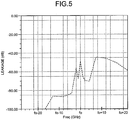
- Figs. 5 and 6 show characteristics of simulations of a level of leakage of spurious to the outside when a length of the wire 6 is ⁇ /4, i.e., characteristics of simulations of passage of a radio-frequency component in an area between the wire 6 and the external conductor pad 21.
- the leading-end open line 50 is not provided.
- the leading-end open line 50 in length of ⁇ /4 is provided.
- fo indicates a frequency of the spurious emission.
- the seal ring 3 and the cover 4 which are separate parts, are employed.
- a cap member that the seal ring 3 and the cover 4 are integrally molded thereinto can be employed as the electromagnetic shield member.
- the leading-end open line having the length equivalent to substantially a quarter of a wavelength of spurious coupled to the wire 6 is provided to the internal conductor pad 5 for bias/control signal, so that the spurious coupled to the wire 6 is reflected by the leading-end open line provided to the internal conductor pad. Therefore, it is possible to reduce a level of spurious coupled to the wire 6, and thus it is possible to reduce a level of spurious leaking to the outside. Consequently, it is possible to suppress leakage of spurious to outside the radio-frequency package reliably. In this manner, within the radio-frequency package, leakage of a radio-frequency component to outside the radio-frequency package can be suppressed, so that it is possible to reduce a production cost.
- the radio-frequency package according to the present invention is useful as a radio-frequency package that a radio-frequency device operating in a microwave band or a millimeter-wave band is mounted in an electromagnetic shield space thereof.
Landscapes
- Shielding Devices Or Components To Electric Or Magnetic Fields (AREA)
Claims (2)
- Hochfrequenzeinheit, umfassend:eine Hochfrequenzvorrichtung (2);ein mehrlagiges dielektrisches Substrat (20) mit einer Oberflächenschicht, auf der die Hochfrequenzvorrichtung (2) angebracht ist; undein elektromagnetisches Abschirmungsteil (3, 4), das einen Teil der Oberflächenschicht des mehrlagigen dielektrischen Substrats (20) und der Hochfrequenzvorrichtung (2) bedeckt, wobei das mehrlagige dielektrische Substrat (20) eine interne Leiterkontaktfläche für ein Vorspannungs-/Steuersignal (5) umfasst, der auf der Oberflächenschicht des mehrlagigen dielektrischen Substrats (20) im Inneren des elektromagnetischen Abschirmungsteils (3, 4) angeordnet und mit der Hochfrequenzvorrichtung (2) leitend verbunden ist,eine erste Signal-Durchgangsöffnung (24), die an die interne Leiterkontaktfläche (5) angeschlossen und im Inneren des elektromagnetischen Abschirmungsteils (3, 4) angeordnet ist,eine externe Leiterkontaktfläche für ein Vorspannungs-/Steuersignal (21), der außerhalb des elektromagnetischen Abschirmungsteils (3, 4) angeordnet ist,eine zweite Signal-Durchgangsöffnung (22), die an die externe Leiterkontaktfläche (21) angeschlossen und außerhalb des elektromagnetischen Abschirmungsteils (3, 4) angeordnet ist, undeine Innenschicht-Signalleitung (23), die eine Verbindung zwischen der ersten Signal-Durchgangsöffnung (24) und der zweiten Signal-Durchgangsöffnung (22) herstellt, unddadurch gekennzeichnet, dassdie interne Leiterkontaktfläche (5) eine am Vorlaufende offene Leitung (50) mit einer Länge eines Viertels einer Wellenlänge eines in der Hochfrequenzvorrichtung (2) verwendeten Hochfrequenzsignals umfasst.
- Hochfrequenzeinheit nach Anspruch 1, wobei die am Vorlaufende offene Leitung (50) eine Länge eines Viertels der Wellenlänge des Hochfrequenzsignals aus der ersten Signal-Durchgangsöffnung (24) hat.
Applications Claiming Priority (2)
| Application Number | Priority Date | Filing Date | Title |
|---|---|---|---|
| JP2007065475 | 2007-03-14 | ||
| PCT/JP2008/053292 WO2008111391A1 (ja) | 2007-03-14 | 2008-02-26 | 高周波パッケージ |
Publications (3)
| Publication Number | Publication Date |
|---|---|
| EP2124253A1 EP2124253A1 (de) | 2009-11-25 |
| EP2124253A4 EP2124253A4 (de) | 2010-08-04 |
| EP2124253B1 true EP2124253B1 (de) | 2019-05-22 |
Family
ID=39759333
Family Applications (1)
| Application Number | Title | Priority Date | Filing Date |
|---|---|---|---|
| EP08720878.1A Active EP2124253B1 (de) | 2007-03-14 | 2008-02-26 | Hochfrequenzkapselung |
Country Status (5)
| Country | Link |
|---|---|
| US (1) | US8130513B2 (de) |
| EP (1) | EP2124253B1 (de) |
| JP (1) | JP4990353B2 (de) |
| CN (1) | CN101578697B (de) |
| WO (1) | WO2008111391A1 (de) |
Families Citing this family (12)
| Publication number | Priority date | Publication date | Assignee | Title |
|---|---|---|---|---|
| JP4942776B2 (ja) * | 2009-01-23 | 2012-05-30 | 日立オートモティブシステムズ株式会社 | 電子デバイスパッケージ構造及びそれが用いられた電子回路モジュール |
| JP5093137B2 (ja) * | 2009-02-02 | 2012-12-05 | 三菱電機株式会社 | 高周波モジュール |
| US8110915B2 (en) * | 2009-10-16 | 2012-02-07 | Infineon Technologies Ag | Open cavity leadless surface mountable package for high power RF applications |
| JP5512566B2 (ja) * | 2011-01-31 | 2014-06-04 | 株式会社東芝 | 半導体装置 |
| WO2012160837A1 (ja) * | 2011-05-24 | 2012-11-29 | 三菱電機株式会社 | 高周波パッケージ |
| CN103151340B (zh) * | 2013-02-08 | 2016-04-20 | 日月光半导体制造股份有限公司 | 天线封装模块及其制造方法 |
| JP5728102B1 (ja) * | 2014-02-13 | 2015-06-03 | 日本電信電話株式会社 | Mmic集積回路モジュール |
| US9583811B2 (en) * | 2014-08-07 | 2017-02-28 | Infineon Technologies Ag | Transition between a plastic waveguide and a semiconductor chip, where the semiconductor chip is embedded and encapsulated within a mold compound |
| CN106952886B (zh) * | 2017-03-25 | 2019-08-09 | 华进半导体封装先导技术研发中心有限公司 | 一种射频芯片封装结构 |
| US11152707B1 (en) * | 2020-07-02 | 2021-10-19 | International Business Machines Corporation | Fast radio frequency package |
| CN118120049A (zh) * | 2021-10-13 | 2024-05-31 | 三菱电机株式会社 | 高频半导体封装 |
| KR102722385B1 (ko) * | 2021-11-04 | 2024-10-25 | 주식회사 웨이브피아 | 알에프 칩 패키지 |
Family Cites Families (25)
| Publication number | Priority date | Publication date | Assignee | Title |
|---|---|---|---|---|
| US5045820A (en) * | 1989-09-27 | 1991-09-03 | Motorola, Inc. | Three-dimensional microwave circuit carrier and integral waveguide coupler |
| JPH04186645A (ja) | 1990-11-16 | 1992-07-03 | Sanyo Electric Co Ltd | マイクロ波集積回路の製造方法 |
| JPH04363901A (ja) | 1990-11-26 | 1992-12-16 | Mitsubishi Materials Corp | 高周波、マイクロ波用混成集積回路及びその製造方法 |
| JP2823461B2 (ja) | 1992-12-11 | 1998-11-11 | 三菱電機株式会社 | 高周波帯ic用パッケージ |
| JP3147019B2 (ja) | 1997-02-07 | 2001-03-19 | 日本電気株式会社 | 高周波回路 |
| JP3209183B2 (ja) | 1998-07-08 | 2001-09-17 | 日本電気株式会社 | 高周波信号用集積回路パッケージ及びその製造方法 |
| JP2003086728A (ja) * | 2001-07-05 | 2003-03-20 | Matsushita Electric Ind Co Ltd | 高周波回路の製作方法及びそれを用いた装置 |
| US6936917B2 (en) * | 2001-09-26 | 2005-08-30 | Molex Incorporated | Power delivery connector for integrated circuits utilizing integrated capacitors |
| JP3766791B2 (ja) * | 2001-10-12 | 2006-04-19 | シャープ株式会社 | 高周波フィルタ回路および高周波通信装置 |
| US6914481B2 (en) * | 2001-11-26 | 2005-07-05 | Matsushita Electric Industrial Co., Ltd. | High frequency power amplifier apparatus and power amplifier module use the same |
| JP3778075B2 (ja) * | 2001-12-12 | 2006-05-24 | ソニー株式会社 | フィルタ回路 |
| JP3649183B2 (ja) * | 2001-12-27 | 2005-05-18 | ソニー株式会社 | フィルタ回路装置及びその製造方法 |
| US7102458B2 (en) * | 2002-05-23 | 2006-09-05 | Kyocera Corporation | High-frequency line-waveguide converter having the HF line terminated within an opening portion |
| JP3738755B2 (ja) * | 2002-08-01 | 2006-01-25 | 日本電気株式会社 | チップ部品を備える電子装置 |
| US7276987B2 (en) * | 2002-10-29 | 2007-10-02 | Kyocera Corporation | High frequency line-to-waveguide converter and high frequency package |
| JP4186645B2 (ja) | 2003-02-24 | 2008-11-26 | 松下電器産業株式会社 | 超音波流量計測装置 |
| JP4363901B2 (ja) | 2003-06-02 | 2009-11-11 | 株式会社フジタ | 電磁波吸収パネルの製作方法及び電磁波吸収パネル |
| JP3895716B2 (ja) | 2003-09-24 | 2007-03-22 | 三菱電機株式会社 | 高周波伝送基板および高周波伝送基板接続構造 |
| JP2005198051A (ja) * | 2004-01-08 | 2005-07-21 | Hitachi Ltd | 高周波モジュール |
| US7336221B2 (en) * | 2004-03-26 | 2008-02-26 | Mitsubishi Denki Kabushiki Kaisha | High frequency package, transmitting and receiving module and wireless equipment |
| JP4056500B2 (ja) * | 2004-06-28 | 2008-03-05 | 三菱電機株式会社 | 伝送線路基板および半導体パッケージ |
| WO2006001389A1 (ja) * | 2004-06-28 | 2006-01-05 | Mitsubishi Denki Kabushiki Kaisha | 多層誘電体基板および半導体パッケージ |
| CN101015118A (zh) * | 2004-09-21 | 2007-08-08 | 株式会社村田制作所 | 高频振荡电路和收发装置 |
| US8040286B2 (en) * | 2006-02-06 | 2011-10-18 | Mitsubishi Electric Corporation | High frequency module |
| CA2650496C (en) * | 2006-04-26 | 2016-06-28 | Ems Technologies, Inc. | Planar mixed-signal circuit board |
-
2008
- 2008-02-26 JP JP2009503955A patent/JP4990353B2/ja not_active Expired - Fee Related
- 2008-02-26 CN CN2008800017522A patent/CN101578697B/zh not_active Expired - Fee Related
- 2008-02-26 US US12/519,861 patent/US8130513B2/en not_active Expired - Fee Related
- 2008-02-26 WO PCT/JP2008/053292 patent/WO2008111391A1/ja not_active Ceased
- 2008-02-26 EP EP08720878.1A patent/EP2124253B1/de active Active
Also Published As
| Publication number | Publication date |
|---|---|
| CN101578697A (zh) | 2009-11-11 |
| EP2124253A4 (de) | 2010-08-04 |
| JPWO2008111391A1 (ja) | 2010-06-24 |
| JP4990353B2 (ja) | 2012-08-01 |
| US8130513B2 (en) | 2012-03-06 |
| EP2124253A1 (de) | 2009-11-25 |
| US20100046184A1 (en) | 2010-02-25 |
| WO2008111391A1 (ja) | 2008-09-18 |
| CN101578697B (zh) | 2011-12-28 |
Similar Documents
| Publication | Publication Date | Title |
|---|---|---|
| EP2124253B1 (de) | Hochfrequenzkapselung | |
| US7336221B2 (en) | High frequency package, transmitting and receiving module and wireless equipment | |
| EP1777775B1 (de) | Übertragungsleitungsträger und halbleitergehäuse | |
| US10262957B2 (en) | Millimeter wave integrated circuit with ball grid array package including transmit and receive channels | |
| JP4861303B2 (ja) | レーダセンサ | |
| JP4523223B2 (ja) | レーダセンサ | |
| EP1775765A1 (de) | Mehrschichtiges dielektrisches substrat und halbleiterkapselung | |
| US8362608B2 (en) | Ultra wideband hermetically sealed surface mount technology for microwave monolithic integrated circuit package | |
| JP5566933B2 (ja) | 高周波通信装置 | |
| CN1714467A (zh) | 应用于毫米频率的封装电子器件 | |
| EP1462822A1 (de) | Mobiler millimeterwellenradar | |
| JP4634836B2 (ja) | 高周波パッケージ、送受信モジュールおよび無線装置 | |
| EP2284881B1 (de) | Hochfrequenzmodul mit einem gehäuse und mehreren hochfrequenzschaltkreisen | |
| JP2008244289A (ja) | 電磁シールド構造 | |
| JP4634837B2 (ja) | 高周波パッケージ、送受信モジュールおよび無線装置 | |
| EP1480289A1 (de) | Elektronisches Komponenten-Modul | |
| US11343912B2 (en) | Electronic circuit apparatus | |
| JP2012227434A (ja) | 高周波パッケージ | |
| HK1086950B (en) | Packaged electronic component for applications at millimetric frequencies |
Legal Events
| Date | Code | Title | Description |
|---|---|---|---|
| PUAI | Public reference made under article 153(3) epc to a published international application that has entered the european phase |
Free format text: ORIGINAL CODE: 0009012 |
|
| 17P | Request for examination filed |
Effective date: 20090910 |
|
| AK | Designated contracting states |
Kind code of ref document: A1 Designated state(s): AT BE BG CH CY CZ DE DK EE ES FI FR GB GR HR HU IE IS IT LI LT LU LV MC MT NL NO PL PT RO SE SI SK TR |
|
| DAX | Request for extension of the european patent (deleted) | ||
| A4 | Supplementary search report drawn up and despatched |
Effective date: 20100707 |
|
| RIC1 | Information provided on ipc code assigned before grant |
Ipc: H01P 5/02 20060101ALI20100701BHEP Ipc: H01P 1/00 20060101ALI20100701BHEP Ipc: H01L 21/60 20060101AFI20081003BHEP Ipc: H01L 23/66 20060101ALI20100701BHEP Ipc: H01L 23/02 20060101ALI20100701BHEP Ipc: H01L 23/12 20060101ALI20100701BHEP |
|
| 17Q | First examination report despatched |
Effective date: 20110315 |
|
| APBK | Appeal reference recorded |
Free format text: ORIGINAL CODE: EPIDOSNREFNE |
|
| APBN | Date of receipt of notice of appeal recorded |
Free format text: ORIGINAL CODE: EPIDOSNNOA2E |
|
| APBR | Date of receipt of statement of grounds of appeal recorded |
Free format text: ORIGINAL CODE: EPIDOSNNOA3E |
|
| APAF | Appeal reference modified |
Free format text: ORIGINAL CODE: EPIDOSCREFNE |
|
| APBT | Appeal procedure closed |
Free format text: ORIGINAL CODE: EPIDOSNNOA9E |
|
| GRAP | Despatch of communication of intention to grant a patent |
Free format text: ORIGINAL CODE: EPIDOSNIGR1 |
|
| STAA | Information on the status of an ep patent application or granted ep patent |
Free format text: STATUS: GRANT OF PATENT IS INTENDED |
|
| INTG | Intention to grant announced |
Effective date: 20181205 |
|
| RIN1 | Information on inventor provided before grant (corrected) |
Inventor name: YASOOKA, KOUSUKE |
|
| GRAS | Grant fee paid |
Free format text: ORIGINAL CODE: EPIDOSNIGR3 |
|
| GRAA | (expected) grant |
Free format text: ORIGINAL CODE: 0009210 |
|
| STAA | Information on the status of an ep patent application or granted ep patent |
Free format text: STATUS: THE PATENT HAS BEEN GRANTED |
|
| AK | Designated contracting states |
Kind code of ref document: B1 Designated state(s): AT BE BG CH CY CZ DE DK EE ES FI FR GB GR HR HU IE IS IT LI LT LU LV MC MT NL NO PL PT RO SE SI SK TR |
|
| REG | Reference to a national code |
Ref country code: GB Ref legal event code: FG4D |
|
| REG | Reference to a national code |
Ref country code: CH Ref legal event code: EP |
|
| REG | Reference to a national code |
Ref country code: IE Ref legal event code: FG4D |
|
| REG | Reference to a national code |
Ref country code: DE Ref legal event code: R096 Ref document number: 602008060160 Country of ref document: DE |
|
| REG | Reference to a national code |
Ref country code: AT Ref legal event code: REF Ref document number: 1137120 Country of ref document: AT Kind code of ref document: T Effective date: 20190615 |
|
| REG | Reference to a national code |
Ref country code: NL Ref legal event code: MP Effective date: 20190522 |
|
| REG | Reference to a national code |
Ref country code: LT Ref legal event code: MG4D |
|
| PG25 | Lapsed in a contracting state [announced via postgrant information from national office to epo] |
Ref country code: SE Free format text: LAPSE BECAUSE OF FAILURE TO SUBMIT A TRANSLATION OF THE DESCRIPTION OR TO PAY THE FEE WITHIN THE PRESCRIBED TIME-LIMIT Effective date: 20190522 Ref country code: HR Free format text: LAPSE BECAUSE OF FAILURE TO SUBMIT A TRANSLATION OF THE DESCRIPTION OR TO PAY THE FEE WITHIN THE PRESCRIBED TIME-LIMIT Effective date: 20190522 Ref country code: LT Free format text: LAPSE BECAUSE OF FAILURE TO SUBMIT A TRANSLATION OF THE DESCRIPTION OR TO PAY THE FEE WITHIN THE PRESCRIBED TIME-LIMIT Effective date: 20190522 Ref country code: ES Free format text: LAPSE BECAUSE OF FAILURE TO SUBMIT A TRANSLATION OF THE DESCRIPTION OR TO PAY THE FEE WITHIN THE PRESCRIBED TIME-LIMIT Effective date: 20190522 Ref country code: NL Free format text: LAPSE BECAUSE OF FAILURE TO SUBMIT A TRANSLATION OF THE DESCRIPTION OR TO PAY THE FEE WITHIN THE PRESCRIBED TIME-LIMIT Effective date: 20190522 Ref country code: NO Free format text: LAPSE BECAUSE OF FAILURE TO SUBMIT A TRANSLATION OF THE DESCRIPTION OR TO PAY THE FEE WITHIN THE PRESCRIBED TIME-LIMIT Effective date: 20190822 Ref country code: FI Free format text: LAPSE BECAUSE OF FAILURE TO SUBMIT A TRANSLATION OF THE DESCRIPTION OR TO PAY THE FEE WITHIN THE PRESCRIBED TIME-LIMIT Effective date: 20190522 Ref country code: PT Free format text: LAPSE BECAUSE OF FAILURE TO SUBMIT A TRANSLATION OF THE DESCRIPTION OR TO PAY THE FEE WITHIN THE PRESCRIBED TIME-LIMIT Effective date: 20190922 |
|
| PG25 | Lapsed in a contracting state [announced via postgrant information from national office to epo] |
Ref country code: BG Free format text: LAPSE BECAUSE OF FAILURE TO SUBMIT A TRANSLATION OF THE DESCRIPTION OR TO PAY THE FEE WITHIN THE PRESCRIBED TIME-LIMIT Effective date: 20190822 Ref country code: LV Free format text: LAPSE BECAUSE OF FAILURE TO SUBMIT A TRANSLATION OF THE DESCRIPTION OR TO PAY THE FEE WITHIN THE PRESCRIBED TIME-LIMIT Effective date: 20190522 Ref country code: GR Free format text: LAPSE BECAUSE OF FAILURE TO SUBMIT A TRANSLATION OF THE DESCRIPTION OR TO PAY THE FEE WITHIN THE PRESCRIBED TIME-LIMIT Effective date: 20190823 |
|
| REG | Reference to a national code |
Ref country code: AT Ref legal event code: MK05 Ref document number: 1137120 Country of ref document: AT Kind code of ref document: T Effective date: 20190522 |
|
| PG25 | Lapsed in a contracting state [announced via postgrant information from national office to epo] |
Ref country code: DK Free format text: LAPSE BECAUSE OF FAILURE TO SUBMIT A TRANSLATION OF THE DESCRIPTION OR TO PAY THE FEE WITHIN THE PRESCRIBED TIME-LIMIT Effective date: 20190522 Ref country code: AT Free format text: LAPSE BECAUSE OF FAILURE TO SUBMIT A TRANSLATION OF THE DESCRIPTION OR TO PAY THE FEE WITHIN THE PRESCRIBED TIME-LIMIT Effective date: 20190522 Ref country code: CZ Free format text: LAPSE BECAUSE OF FAILURE TO SUBMIT A TRANSLATION OF THE DESCRIPTION OR TO PAY THE FEE WITHIN THE PRESCRIBED TIME-LIMIT Effective date: 20190522 Ref country code: SK Free format text: LAPSE BECAUSE OF FAILURE TO SUBMIT A TRANSLATION OF THE DESCRIPTION OR TO PAY THE FEE WITHIN THE PRESCRIBED TIME-LIMIT Effective date: 20190522 Ref country code: RO Free format text: LAPSE BECAUSE OF FAILURE TO SUBMIT A TRANSLATION OF THE DESCRIPTION OR TO PAY THE FEE WITHIN THE PRESCRIBED TIME-LIMIT Effective date: 20190522 Ref country code: EE Free format text: LAPSE BECAUSE OF FAILURE TO SUBMIT A TRANSLATION OF THE DESCRIPTION OR TO PAY THE FEE WITHIN THE PRESCRIBED TIME-LIMIT Effective date: 20190522 |
|
| REG | Reference to a national code |
Ref country code: DE Ref legal event code: R097 Ref document number: 602008060160 Country of ref document: DE |
|
| PG25 | Lapsed in a contracting state [announced via postgrant information from national office to epo] |
Ref country code: IT Free format text: LAPSE BECAUSE OF FAILURE TO SUBMIT A TRANSLATION OF THE DESCRIPTION OR TO PAY THE FEE WITHIN THE PRESCRIBED TIME-LIMIT Effective date: 20190522 |
|
| PLBE | No opposition filed within time limit |
Free format text: ORIGINAL CODE: 0009261 |
|
| STAA | Information on the status of an ep patent application or granted ep patent |
Free format text: STATUS: NO OPPOSITION FILED WITHIN TIME LIMIT |
|
| PG25 | Lapsed in a contracting state [announced via postgrant information from national office to epo] |
Ref country code: TR Free format text: LAPSE BECAUSE OF FAILURE TO SUBMIT A TRANSLATION OF THE DESCRIPTION OR TO PAY THE FEE WITHIN THE PRESCRIBED TIME-LIMIT Effective date: 20190522 |
|
| 26N | No opposition filed |
Effective date: 20200225 |
|
| PG25 | Lapsed in a contracting state [announced via postgrant information from national office to epo] |
Ref country code: PL Free format text: LAPSE BECAUSE OF FAILURE TO SUBMIT A TRANSLATION OF THE DESCRIPTION OR TO PAY THE FEE WITHIN THE PRESCRIBED TIME-LIMIT Effective date: 20190522 |
|
| PG25 | Lapsed in a contracting state [announced via postgrant information from national office to epo] |
Ref country code: SI Free format text: LAPSE BECAUSE OF FAILURE TO SUBMIT A TRANSLATION OF THE DESCRIPTION OR TO PAY THE FEE WITHIN THE PRESCRIBED TIME-LIMIT Effective date: 20190522 |
|
| REG | Reference to a national code |
Ref country code: CH Ref legal event code: PL |
|
| GBPC | Gb: european patent ceased through non-payment of renewal fee |
Effective date: 20200226 |
|
| REG | Reference to a national code |
Ref country code: BE Ref legal event code: MM Effective date: 20200229 |
|
| PG25 | Lapsed in a contracting state [announced via postgrant information from national office to epo] |
Ref country code: MC Free format text: LAPSE BECAUSE OF FAILURE TO SUBMIT A TRANSLATION OF THE DESCRIPTION OR TO PAY THE FEE WITHIN THE PRESCRIBED TIME-LIMIT Effective date: 20190522 Ref country code: LU Free format text: LAPSE BECAUSE OF NON-PAYMENT OF DUE FEES Effective date: 20200226 |
|
| PG25 | Lapsed in a contracting state [announced via postgrant information from national office to epo] |
Ref country code: CH Free format text: LAPSE BECAUSE OF NON-PAYMENT OF DUE FEES Effective date: 20200229 Ref country code: LI Free format text: LAPSE BECAUSE OF NON-PAYMENT OF DUE FEES Effective date: 20200229 |
|
| PG25 | Lapsed in a contracting state [announced via postgrant information from national office to epo] |
Ref country code: FR Free format text: LAPSE BECAUSE OF NON-PAYMENT OF DUE FEES Effective date: 20200229 Ref country code: IE Free format text: LAPSE BECAUSE OF NON-PAYMENT OF DUE FEES Effective date: 20200226 Ref country code: GB Free format text: LAPSE BECAUSE OF NON-PAYMENT OF DUE FEES Effective date: 20200226 |
|
| PG25 | Lapsed in a contracting state [announced via postgrant information from national office to epo] |
Ref country code: BE Free format text: LAPSE BECAUSE OF NON-PAYMENT OF DUE FEES Effective date: 20200229 |
|
| PGFP | Annual fee paid to national office [announced via postgrant information from national office to epo] |
Ref country code: DE Payment date: 20220105 Year of fee payment: 15 |
|
| PG25 | Lapsed in a contracting state [announced via postgrant information from national office to epo] |
Ref country code: MT Free format text: LAPSE BECAUSE OF FAILURE TO SUBMIT A TRANSLATION OF THE DESCRIPTION OR TO PAY THE FEE WITHIN THE PRESCRIBED TIME-LIMIT Effective date: 20190522 Ref country code: CY Free format text: LAPSE BECAUSE OF FAILURE TO SUBMIT A TRANSLATION OF THE DESCRIPTION OR TO PAY THE FEE WITHIN THE PRESCRIBED TIME-LIMIT Effective date: 20190522 |
|
| PG25 | Lapsed in a contracting state [announced via postgrant information from national office to epo] |
Ref country code: IS Free format text: LAPSE BECAUSE OF FAILURE TO SUBMIT A TRANSLATION OF THE DESCRIPTION OR TO PAY THE FEE WITHIN THE PRESCRIBED TIME-LIMIT Effective date: 20190922 |
|
| REG | Reference to a national code |
Ref country code: DE Ref legal event code: R119 Ref document number: 602008060160 Country of ref document: DE |
|
| PG25 | Lapsed in a contracting state [announced via postgrant information from national office to epo] |
Ref country code: DE Free format text: LAPSE BECAUSE OF NON-PAYMENT OF DUE FEES Effective date: 20230901 |