EP2124346A2 - Verstärker mit Leistungsrückgewinnung aus einer Schmalbandantenne - Google Patents
Verstärker mit Leistungsrückgewinnung aus einer Schmalbandantenne Download PDFInfo
- Publication number
- EP2124346A2 EP2124346A2 EP09160880A EP09160880A EP2124346A2 EP 2124346 A2 EP2124346 A2 EP 2124346A2 EP 09160880 A EP09160880 A EP 09160880A EP 09160880 A EP09160880 A EP 09160880A EP 2124346 A2 EP2124346 A2 EP 2124346A2
- Authority
- EP
- European Patent Office
- Prior art keywords
- antenna
- state
- transistors
- amplifier
- signal
- Prior art date
- Legal status (The legal status is an assumption and is not a legal conclusion. Google has not performed a legal analysis and makes no representation as to the accuracy of the status listed.)
- Granted
Links
Images




Classifications
-
- H—ELECTRICITY
- H04—ELECTRIC COMMUNICATION TECHNIQUE
- H04B—TRANSMISSION
- H04B1/00—Details of transmission systems, not covered by a single one of groups H04B3/00 - H04B13/00; Details of transmission systems not characterised by the medium used for transmission
- H04B1/02—Transmitters
- H04B1/04—Circuits
- H04B1/0458—Arrangements for matching and coupling between power amplifier and antenna or between amplifying stages
-
- G—PHYSICS
- G01—MEASURING; TESTING
- G01S—RADIO DIRECTION-FINDING; RADIO NAVIGATION; DETERMINING DISTANCE OR VELOCITY BY USE OF RADIO WAVES; LOCATING OR PRESENCE-DETECTING BY USE OF THE REFLECTION OR RERADIATION OF RADIO WAVES; ANALOGOUS ARRANGEMENTS USING OTHER WAVES
- G01S1/00—Beacons or beacon systems transmitting signals having a characteristic or characteristics capable of being detected by non-directional receivers and defining directions, positions, or position lines fixed relatively to the beacon transmitters; Receivers co-operating therewith
- G01S1/02—Beacons or beacon systems transmitting signals having a characteristic or characteristics capable of being detected by non-directional receivers and defining directions, positions, or position lines fixed relatively to the beacon transmitters; Receivers co-operating therewith using radio waves
- G01S1/022—Means for monitoring or calibrating
- G01S1/024—Means for monitoring or calibrating of beacon transmitters
-
- G—PHYSICS
- G01—MEASURING; TESTING
- G01S—RADIO DIRECTION-FINDING; RADIO NAVIGATION; DETERMINING DISTANCE OR VELOCITY BY USE OF RADIO WAVES; LOCATING OR PRESENCE-DETECTING BY USE OF THE REFLECTION OR RERADIATION OF RADIO WAVES; ANALOGOUS ARRANGEMENTS USING OTHER WAVES
- G01S1/00—Beacons or beacon systems transmitting signals having a characteristic or characteristics capable of being detected by non-directional receivers and defining directions, positions, or position lines fixed relatively to the beacon transmitters; Receivers co-operating therewith
- G01S1/02—Beacons or beacon systems transmitting signals having a characteristic or characteristics capable of being detected by non-directional receivers and defining directions, positions, or position lines fixed relatively to the beacon transmitters; Receivers co-operating therewith using radio waves
- G01S1/04—Details
- G01S1/042—Transmitters
- G01S1/0423—Mounting or deployment thereof
-
- G—PHYSICS
- G01—MEASURING; TESTING
- G01S—RADIO DIRECTION-FINDING; RADIO NAVIGATION; DETERMINING DISTANCE OR VELOCITY BY USE OF RADIO WAVES; LOCATING OR PRESENCE-DETECTING BY USE OF THE REFLECTION OR RERADIATION OF RADIO WAVES; ANALOGOUS ARRANGEMENTS USING OTHER WAVES
- G01S1/00—Beacons or beacon systems transmitting signals having a characteristic or characteristics capable of being detected by non-directional receivers and defining directions, positions, or position lines fixed relatively to the beacon transmitters; Receivers co-operating therewith
- G01S1/02—Beacons or beacon systems transmitting signals having a characteristic or characteristics capable of being detected by non-directional receivers and defining directions, positions, or position lines fixed relatively to the beacon transmitters; Receivers co-operating therewith using radio waves
- G01S1/08—Systems for determining direction or position line
- G01S1/20—Systems for determining direction or position line using a comparison of transit time of synchronised signals transmitted from non-directional antennas or antenna systems spaced apart, i.e. path-difference systems
- G01S1/24—Systems for determining direction or position line using a comparison of transit time of synchronised signals transmitted from non-directional antennas or antenna systems spaced apart, i.e. path-difference systems the synchronised signals being pulses or equivalent modulations on carrier waves and the transit times being compared by measuring the difference in arrival time of a significant part of the modulations, e.g. LORAN systems
-
- H—ELECTRICITY
- H03—ELECTRONIC CIRCUITRY
- H03F—AMPLIFIERS
- H03F1/00—Details of amplifiers with only discharge tubes, only semiconductor devices or only unspecified devices as amplifying elements
- H03F1/02—Modifications of amplifiers to raise the efficiency, e.g. gliding Class A stages, use of an auxiliary oscillation
-
- H—ELECTRICITY
- H03—ELECTRONIC CIRCUITRY
- H03F—AMPLIFIERS
- H03F1/00—Details of amplifiers with only discharge tubes, only semiconductor devices or only unspecified devices as amplifying elements
- H03F1/56—Modifications of input or output impedances, not otherwise provided for
-
- H—ELECTRICITY
- H03—ELECTRONIC CIRCUITRY
- H03F—AMPLIFIERS
- H03F3/00—Amplifiers with only discharge tubes or only semiconductor devices as amplifying elements
- H03F3/20—Power amplifiers, e.g. Class B amplifiers, Class C amplifiers
- H03F3/21—Power amplifiers, e.g. Class B amplifiers, Class C amplifiers with semiconductor devices only
- H03F3/211—Power amplifiers, e.g. Class B amplifiers, Class C amplifiers with semiconductor devices only using a combination of several amplifiers
-
- H—ELECTRICITY
- H03—ELECTRONIC CIRCUITRY
- H03F—AMPLIFIERS
- H03F3/00—Amplifiers with only discharge tubes or only semiconductor devices as amplifying elements
- H03F3/20—Power amplifiers, e.g. Class B amplifiers, Class C amplifiers
- H03F3/21—Power amplifiers, e.g. Class B amplifiers, Class C amplifiers with semiconductor devices only
- H03F3/217—Class D power amplifiers; Switching amplifiers
- H03F3/2173—Class D power amplifiers; Switching amplifiers of the bridge type
-
- H—ELECTRICITY
- H03—ELECTRONIC CIRCUITRY
- H03F—AMPLIFIERS
- H03F3/00—Amplifiers with only discharge tubes or only semiconductor devices as amplifying elements
- H03F3/20—Power amplifiers, e.g. Class B amplifiers, Class C amplifiers
- H03F3/24—Power amplifiers, e.g. Class B amplifiers, Class C amplifiers of transmitter output stages
-
- H—ELECTRICITY
- H03—ELECTRONIC CIRCUITRY
- H03F—AMPLIFIERS
- H03F2200/00—Indexing scheme relating to amplifiers
- H03F2200/387—A circuit being added at the output of an amplifier to adapt the output impedance of the amplifier
-
- H—ELECTRICITY
- H03—ELECTRONIC CIRCUITRY
- H03F—AMPLIFIERS
- H03F2200/00—Indexing scheme relating to amplifiers
- H03F2200/451—Indexing scheme relating to amplifiers the amplifier being a radio frequency amplifier
-
- H—ELECTRICITY
- H03—ELECTRONIC CIRCUITRY
- H03F—AMPLIFIERS
- H03F2200/00—Indexing scheme relating to amplifiers
- H03F2200/537—A transformer being used as coupling element between two amplifying stages
-
- H—ELECTRICITY
- H03—ELECTRONIC CIRCUITRY
- H03F—AMPLIFIERS
- H03F2200/00—Indexing scheme relating to amplifiers
- H03F2200/541—Transformer coupled at the output of an amplifier
-
- H—ELECTRICITY
- H04—ELECTRIC COMMUNICATION TECHNIQUE
- H04B—TRANSMISSION
- H04B1/00—Details of transmission systems, not covered by a single one of groups H04B3/00 - H04B13/00; Details of transmission systems not characterised by the medium used for transmission
- H04B1/02—Transmitters
- H04B1/04—Circuits
- H04B2001/0408—Circuits with power amplifiers
- H04B2001/045—Circuits with power amplifiers with means for improving efficiency
Definitions
- the invention relates to radio frequency signal transmission amplifiers. More specifically, it relates to amplifiers in transmitters where the antenna has relatively short electrical lengths when compared to the transmitted wavelength.
- Loran antennas used in most transmission sites are characterized by having relatively short electrical lengths compared to the transmitted wavelength.
- the antenna highly capacitive due to the short electrical length, is normally series resonated with a loading inductor to minimize the reactance at the center frequency.
- the resulting tuned circuit has a very narrow bandwidth with a quality factor (Q) typically in the range of 20 to 60.
- the ideal transmitted Loran signal has a bandwidth that considerably exceeds the bandwidth of the transmission antenna. It is normally a requirement for any transmitter system that the bandwidth of the antenna exceeds the bandwidth of the transmitted signal. In the case of Loran, the antenna bandwidth deficit makes the antenna unsuitable for a typical transmitter, such as a Long Wave or Medium Wave Amplitude Modulation (AM) simply modified for operation at 100 kHz.
- AM Medium Wave Amplitude Modulation
- AM broadcasting transmitters are designed to operate into constant impedance, typically 50 ohms.
- the concept of impedance implies a steady state relationship between the voltages and currents in the amplifiers and the antenna. With Loran, no such steady state relationship exists.
- the instantaneous impedance of the antenna (the ratio of voltage to current at one instant in time) varies throughout the pulse from a very large level initially to close to the steady state base impedance near the pulse peak, then decreasing and finally becoming negative during the pulse tail.
- the impedance is negative, power is flowing out of the antenna back to the transmitter. The negative power flow necessitates the use of "tail biter" circuitry, currently in use in Loran transmitters.
- AM broadcast transmitters use passive LC impedance matching and combining circuitry to match the antenna impedance to the optimum load impedance for the radio frequency amplifiers. As a result of the considerable change in the antenna impedance during the Loran pulse, passive LC impedance matching networks are not ideal for this situation.
- a method for using an amplifier to recover stored power from an antenna having a short electrical length compared to the transmitted wavelength of a transmitted signal comprising determining an impedance state of the antenna receiving the transmitted signal.
- the amplifier is enabled to a driving state when the impedance state is positive to modulate the signal going to the antenna.
- the amplifier is enabled to a damping state when the impedance state of the antenna is negative, wherein the damping state provides current from the antenna to charge a direct current (DC) power source from power stored in the antenna.
- DC direct current
- an amplitude modulated amplifier for amplifying a radio frequency (RF) signal.
- the amplifier comprising four selectable controllable transistors receiving power from a direct current power supply to amplify the signal, the transistors configured in a bridge configuration with a first and second transistors coupled between the DC power supply and an antenna and a third and fourth transistors coupled between the antenna and ground in an 'H' configuration, each transistor having a gate input to determine the state of the transistor between an on state and an off state.
- each diodes each associated with one of the four transistors forward biased from a source to a drain of each transistor forming a bridge rectifier and drive logic for controlling each of the four transistors from an open state to a closed amplifying state based on external input wherein the drive logic selectable from an active state to a damping state of the amplifier by switching transistors to recover power from the antenna when an impedance state of the antenna is negative and delivering the recovered power to the DC power supply.
- a system for transmitting RF signals comprising a signal source providing a baseband signal to be amplified and modulated before transmission.
- An exciter module is provided for upconverting the signal from the signal source based on a frequency of a received RF source an amplification module comprising one or more of amplifier as described above.
- a power source is provided for delivering DC power to the amplification module or receiving and storing power from the amplification module.
- An antenna coupled to the amplification module is provided where the antenna has a highly capacitive characteristic wherein the signal wavelength is less than the antenna wavelength wherein current is delivered from the amplification module to the antenna when in the driving state and impedance is positive and current is received from the antenna and delivered to the DC power source in the damping state when impedance is negative.
- a controller is coupled to the exciter module, or integrated with the exciter module, for controlling the operation of the one or more amplifiers via the drive logic, wherein a portion of the one or more amplifiers are switched between the driving state or damping state, wherein the remaining amplifiers are placed in an inactive mode, to control the modulation of the transmitted signal.
- the present disclosure provides an amplitude modulated amplifier for Loran signal transmission. Also disclosed is a system for Loran signal transmission using the amplitude modulated amplifier. Embodiments of the present invention are described below, by way of example only, with reference to FIGs. 1-9 .
- the present disclosure provides a modified amplitude modulated amplifier and associated system and method that is designed to accommodate and essentially capture energy flowing from a narrow-band antenna during the negative power flow phase of a signal such as in a Loran pulse.
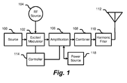
- a suitable transmitter as shown in Figure 1 includes an input source 100, an exciter/modulator 102, an RF source 104, a controller 114, one or more amplifiers 106, a combiner 108, a harmonic filter 110 and a power source 118.
- An antenna 112 is connected to the transmitter to broadcast the signal.
- the input source 100 provides an input signal that is an inphase and quadrature (I, Q) description of the baseband complex envelope.
- the input signal operates through a digital input that carries a baseband representation of the ideal signal to be transmitted. This input would be used when the transmitter operates in the continuous mode. Alternately the transmitter may operate in a pulsed mode where the primary input is used to trigger a pulse from the transmitter and all pulses are the same.
- the pulse shape is stored in the transmitter defining the ideal voltage waveform for a single pulse.
- a DSP based equalizer may be used to determine the necessary amplifier voltage waveform from the desired antenna current waveform when operating in the continuous mode. In the pulse mode the ideal voltage waveform would normally be determined before being stored in the transmitter.
- the Low Frequency (LF) band has a frequency range of 30 kHz to 300 kHz.
- Loran-C and its more modern derivatives are transmitted in the LF band at a centre frequency of 100 kHz.
- the antenna systems used for LF transmission are electrically short because wavelengths are very long and the electrical length of typical antennas is much less than a quarter wave.
- a quarter wave tower would be 750 metres tall.
- a common antenna used by the United States Coast Guard is the 625 foot (190.5 metres) Top Loaded Monopole (TLM) having an electrical length of only 6% of a wavelength.
- TLM Top Loaded Monopole
- a useful factor for characterizing antennas used for LF and Loran transmission is the Q or quality factor.
- the quality factor is the ratio of energy stored in the electric and magnetic fields of the antenna divided by the energy dissipated in the radiation resistance and other losses over a single cycle.
- Q factor f c
- the high Q factor of typical antennas used for Loran is part of what makes transmission difficult and requires analysis for proper system design.
- Impedance measurements at the antenna base can be used to determine Q.
- Two antenna measurements are needed, impedance and reactance slope where reactance is the imaginary part of impedance.
- the antenna can generally be modeled at a particular frequency using a lumped constant series RLC circuit.
- the reactance can be determined as the imaginary part of the impedance as shown in equation 3.
- X ⁇ L - 1 ⁇ C
- the reactance slope may be determined as the derivative of the reactance with respect to frequency as shown in equation 4.
- dX d ⁇ L + 1 C ⁇ ⁇ 2
- the antenna Normally the antenna would be operated at resonance where the inductive reactance and capacitive reactance are equal so that the impedance is purely resistive. For the 625' TLM, the antenna needs to be tuned to resonance by adding an additional 39.8 ⁇ H resulting in a total inductance of 218.8 ⁇ H in the equivalent circuit.
- the quality factor of the antenna can be calculated using equation 7, which is true for the circuit at its resonant frequency. From this equation it is clear that antennas with higher resistance (radiation resistance plus losses in the conduction path including the ground return) will be lower Q and have wider bandwidth.
- Antennas used for Loran transmission are characterized by relatively short electrical lengths when compared to the transmitted wavelength.
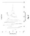
- a time domain representation of a Loran pulse is shown in Figure 2 .
- the next step is to quantify the transient effects based on the specific transmitted waveform and the equivalent circuit that we have developed.
- a frequency transformation of the equivalent circuit from bandpass to lowpass is used.
- the second order antenna equivalent circuit becomes the simplified first order equivalent circuit shown in Figure 6 .
- the lowpass equivalent circuit is governed by the network equation, equation 10.
- V t i t ⁇ R + L ⁇ di dt
- Equation 11 is the result of solving for the lowpass driving voltage needed to give the correct response.
- V t 2 ⁇ Lt - aL ⁇ t 2 + R ⁇ t 2 ⁇ e - at
- the lowpass equivalent circuit must have a 3dB bandwidth which is one half of the 3dB bandwidth of the antenna to achieve the same envelope response.
- the correct lowpass bandwidth is 909 Hz. This specific 3dB bandwidth makes the calculation of L and R straightforward.
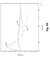
- Figure 4A shows the network response.
- the antenna highly capacitive due to the short electrical length, is normally series resonated with a loading inductor to minimize the reactance at the centre frequency.
- the required driving voltage envelope 400 has a very different envelope than the resulting desired current envelope 402.
- the instantaneous impedance 404 of the antenna (the ratio of voltage to current at one instant in time) varies throughout the pulse from a very large level initially to close to the steady state base impedance near the pulse peak and finally becoming negative during the pulse tail. When the impedance is negative, power is flowing out of the antenna back to the transmitter.
- the current envelope is readily recognizable as a Loran pulse envelope.
- the voltage waveform is very different from the current and is characterized as having a high initial peak followed by a rapid decay and a negative region after the peak of the current waveform.
- the difference between the voltage and current envelope is a key concept in understanding the challenge of Loran transmission systems.
- the voltage peak in this case is approximately five times higher than the current peak, representing an effective "transient voltage factor" (TVF) of five.
- TVF transient voltage factor
- the current waveform and voltage waveforms would be almost the same representing a TVF approaching one.
- the TVF may be used to determine the transmitter peak power capability, for a given antenna and pulse shape. Peak power capability is reduced from its ideal steady state value proportionately to the TVF.
- the very high initial voltage peak shown in Figure 4A provides the power to rapidly increase the stored energy and current in the reactive (lossless) elements of the antenna circuit.
- the majority of the power flowing from the source at the beginning of the pulse is not being dissipated, but stored in the electric and magnetic fields of the antenna.
- the impedance seen by the transmitter varies widely through the pulse.
- the impedance is initially very high, decreases to the steady state value at the current peak and then becomes negative in the pulse tail.
- a broadcast transmitter is not designed for these variations in impedance and would shut down in such a situation.
- An important observation is that after the peak in the current waveform, the stored energy in the antenna circuit must be damped faster than its natural damping rate and the source voltage waveform becomes negative as energy flows from the antenna back to the transmitter.
- the transmitters used in the present system are capable of being modulated by digitally selecting carrier amplifiers.
- an exciter/modulator is placed within the system to modulate the transmitter.
- the actual architecture of the exciter/modulator is not particularly important. Instead, the exciter/modulator should have the following desired features: 1) ability to remove failed amplifiers from the modulation sequence; 2) ability to operate with both pulsed and continuous modulation sequences; 3) enable and disable amplifiers in the pulsed modulation mode following a preset, prequantized sequence; 4) capability of switching the amplifiers between active and passive damping modes, when the modulation is negative; and 5) ability to provide an envelope quantization process for the continuous modulation process.
- the quantization block might also include a randomizer that selects amplifiers randomly in time. The randomization serves to equalize the power delivered by individual amplifiers over time.
- Another possible desired feature of the exciter/modulator is to include a finite impulse response (FIR) equalizer to equalize an external I, Q or input from the continuous modulation sequence.
- FIR finite impulse response
- Transmitters for use in the present system are modulated by digitally selecting carrier amplifiers.
- Class D amplifiers are used as a result of their ability to be modulated by digitally selecting carrier amplifiers.
- a single amplifier can only achieve very limited amplitude modulation.
- a single amplifier effectively has only two states, on or off (active or inactive). The two states only allow for two amplitude levels.
- To modulate a complex waveform, such as Loran more amplitude states are required from the transmitter. Accordingly, some means to allow for a wide range of amplitude modulation must be employed. This can be achieved by using many amplifiers (2 or more) and operating them in the active or inactive states in different ratios at different times (as described in Swanson, United States Patent No. 4,580,111 ), or by using one or more amplifiers and controlling the DC power source voltage (2 in Figure 7A-7G ). It should be noted that there are numerous different ways in which the source voltage could be modulated.
- each amplifier may be operated in one of four modes: inactive mode, active mode, passive damping mode and active damping mode.
- the actual mode of each amplifier can be controlled by the exciter/modulator on each full RF cycle.
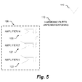
- step modulation (aka digitally selecting carrier amplifiers) is used to achieve amplitude modulation as shown in Figure 5 schematic.
- Step modulation makes use of the fact that a large number of amplifiers must be combined to achieve the high power levels required.
- the exciter On each RF cycle or half RF cycle, the exciter makes a decision on the magnitude of voltage required to achieve the desired RF current waveform and the number of amplifiers operating is adjusted proportionately to the desired voltage waveform. Amplifiers that are not operating on a given RF cycle are in a low-impedance, zero voltage state.
- Figure 5 shows a schematic of a step modulated transmitter using class D amplifiers.
- Amplifier 106 is comprised by multiple amplifiers from 1 to N (122 to 126) to drive a power combiner system composed of a magnetic core and primary winding associated with each individual amplifier, with a single secondary winding combining all the amplifiers outputs in series.
- the combiner output voltage is simply the sum of the input voltages, corrected for the primary to secondary turn ratio of the individual transformers.
- the combined output waveform is then connected to the harmonic filter 550, antenna tuning and antenna circuit and antenna 112. It should be noted that other methods of combining may also be implmeneted.
- the harmonic filter 110 is characterized by series resonant sections in series with the antenna and parallel resonant sections in parallel with the antenna.
- This architecture for the antenna provides for a low-pass filter with very low source impedance and near zero phase delay such that the transmitter behaves as closely as possible to an ideal voltage source.
- the behaviour of a voltage source is desirable as it has ideal transient response which allows for maximum control over the antenna current during the wide range of impedance variations present at the input of the Loran antenna.
- FIG. 6 shows a schematic of an amplifier for recovering power from a narrow-band antenna.
- the operation of each amplifier 122 to 126 is controlled by the combination of an amplifier drive logic 602 and associated circuitry.
- the drive logic 602 and associated circuitry must be able to receive from the exciter at least four signals, namely an RF drive signal 604, an enable signal 606, a damp signal 608 and a phase signal 610, to each amplifier.
- the amplifier design enables instantaneous phase reversal as required by Loran. This is achieved by having an RF phase input which is the control input as well as the separate phase input.
- the ability to put the amplifier into "passive damping mode” enables the antenna to free run so as to minimize losses due to switching the amplifiers and drivers during the period of time that power is recovered from the antenna.
- the drive logic enables control of the transistors so that they are in any state on any cycle.
- the RF drive signal 604 contains the RF phase information from the RF source, namely the desired amplifier voltage zero crossings. For the transmission of a Loran signal, this signal 604 would operate as a continuous 100 kHz square wave with no phase modulation although this signal could be any type of signal. All mode changes are made synchronously with the RF Phase signal 610, which is used as a clock to detect the mode control signals.
- the amplifier itself should contain an adjustable dead time control that allows the dead time to be adjusted to allow for reduction of switching loss.
- the enable signal 606 can be either inactive or active.
- the amplifier When the enable signal 606 is inactive, the amplifier is in a zero voltage, low impedance state with the top two transistors 650, 660 in the bridge in an open or off position and the bottom two transistors 670, 680 in the bridge in the closed or on position.
- the enable signal 606 When the enable signal 606 is active, the amplifier may be in the Active mode, the Passive Damping mode or the Active Damping Mode as determined by the RF drive 604, Damp 608 and Phase 610 Signals.
- the phase signal 610 is used to invert the voltage output of the amplifier with respect to the RF Drive signal 604. During normal Loran operation, the Phase signal 610 would be triggered throughout some of the pulses where a negative phase code pulse was desired. Additionally, if the Phase signal 610 was inverted when current was already flowing in the antenna, the impedance phase would be inverted, i.e. positive impedance to negative impedance, and the amplifier mode would change from Active mode to Active Damping mode.
- the two lower transistors 670, 680 have direct coupled gate drive as their source leads are grounded. Driving these transistors does not require the gate drive to be floated at the B+ voltage source 600.
- the two upper transistors 650, 660 require an isolated gate drive circuit. This isolated gate drive circuit can be achieved by using a transformer 630, 640. When the amplifier is disabled, it is necessary that transistors 650, 660 are off continuously. This requires that the DC voltage be zero.
- two drivers are used for each transformer 630, 640. This improves the gate drive transient response when it is started and stopped due to the amplifier being enabled or disabled.
- the combiner should have output current and voltage transducers for instrumentation, protection and adaptive modulation.
- an impedance matching and harmonic filter is required.
- the antenna system must be inductively loaded such that the antenna and loading inductor together form a series resonant circuit, resonant at the transmitter carrier frequency. Accordingly, a servo controlled variometer or some other means is required to maintain the circuit at the correct resonant frequency.
- the loading inductor circuit should be modified so that suitable modification of the odd harmonics will be provided.
- the power required from the main DC power supply in the present system is relatively low compared to AM and FM broadcasting. Moreover, since the number of amplifiers may be small, the envelope modulation system is not readily adapted to fine regulation. As a result, a regulated B+ power supply is preferred.
- FIG. 7A Schematic representation of the operational states of the amplifier are showing in Figures 7A to 7G .
- Gates 10, 20, 30 and 40 combined with diodes 60, 70, 80 and 90 correspond to transistors 650,660, 670 and 680 respectively of Figure 6 .
- the active mode is characterized by the normal operation where the amplifier is contributing energy to the load or antenna 50 where the voltage and current are in phase as shown in Figures 7A and 7B .
- Two states may be defined for each mode based upon the phase of the signal.
- the voltage applied by the amplifier across the load 50 should be in phase with the current.
- transistors 10 and 40 are closed and transistors 20 and 30 are open as shown in Figure 7A .
- transistors 10 and 40 are open and transistors 20 and 30 are closed as shown in Figure 7B .
- the output voltage of the transmitter is proportional to the number of amplifiers in the active mode.
- the impedance recognized by the amplifier is variable depending on the current at the downstream combiner at that particular moment in time.
- the combiner current is determined by the number of active amplifiers as well as the load Q and the history of modulation.
- the amplifier(s) remain in the active mode as long as the load impedance remains positive and energy flow is into the antenna 50.
- the antenna is causing current to flow in the amplifier (50 is a source of current) and all the transistors 10,20,30, 40 are open. With the transistors 10, 20, 30, 40 open, the rectifiers 60, 70, 80 and 90 act as bridge rectifiers and rectified RF current flows back to the source 2 providing a capacitor 4 for storing power thus absorbing energy from the antenna 50.
- rectifiers 60 and 90 are in conduction and rectifiers 70 and 80 are off as shown in Figure 7C .
- the current flow reverses, rectifiers 70 and 80 are in conduction and rectifiers 60 and 90 are off as shown in Figure 7D .
- the voltage applied to the antenna 50 is proportional to the number of amplifiers in the passive damping mode, but in opposition to current flow making the voltage effectively negative. At this time, the impedance seen by the transmitter is also negative.
- the system can still be voltage modulated, since the output voltage of the transmitter is proportional to the number of amplifiers that are active in the passive damping state.
- phase modulation may be achieved by causing the transistors 10, 20, 30 and 40 to close slightly before, or stay closed slightly longer than the normal rectifier conduction would have occurred in the passive damping mode.
- the ability to provide active damping provides control of the phase as opposed to passive damping where phase control is not maintained.
- the system is still voltage modulated during active damping, since the output voltage of the transmitter is proportional to the number of amplifiers that are active in the active damping state.
- both bottom transistors 30, 40 are continuously on and both top transistors 10, 20 are continuously off. Alternately, both top transistors 10, 20 are continuously on and both bottom transistors 30, 40 are continuously off.
- input signals such as Loran pulses
- both amplifiers within the transmitter are in the inactive mode.
- the alternating radio frequency current from the antenna circulates from the source 50 around a loop composed of transistors 30, 40 and through the ground connection between them. While this current is circulating, the amplifier is neither contributing or absorbing power from the load as the voltage around the loop is very low.
- the primary limitation is that when the antenna current becomes very small it is insufficient to fully charge and discharge the self-capacitance of the transistors used in the class-D amplifier during each RF cycle. As a result the rectifiers never become forward biased allowing power to flow from the antenna back to the power supply. The magnitude of RF antenna current where this effect becomes significant is relatively small so it does not represent a significant energy loss.
- the Loran signal specification requires that the pulse tail current be damped to very low levels at the end of the pulse. These levels are less than the level where the amplifier operates as an effective damping system so another method of pulse damping is required late in the pulse tail.
- one or more amplifiers are modified to operate only as a resistive damping element when required at the end of the pulse.
- the amplifier is modified by removing the connection to the power supply 2 and the top transistors 60 and 70 while adding an appropriate resistor in parallel with the load 50.
- the resistive damping element operates in one of two modes. In the first mode, the inactive mode, transistors 80 and 90 are on and load current circulates from the load through transistors 80 and 90 and the amplifier is effectively out of the circuit. In the active mode transistors 80 and 90 are open and the antenna current flows through the resistor in parallel with the load. In the active mode the resistive damping element effectively places the damping resistor in series with the load current thus damping the antenna current without the limitations described when an amplifier recovers power from the antenna.
- the voltage source needs to be able to operate with a negative voltage after about the 80 microsecond point in the pulse.
- the voltage also needs to be negative for a transmitter operating on the radio frequency signal at 100 kHz. This is achieved when the voltage waveform is inverted and the RF current and voltage at the transmitter output are out of phase.
- the voltage phase reversal can be seen in Figure 8 .
- the absolute efficiency limit for an antenna Q of 55 is 67% and for an antenna Q of 120 the limit is 37%. Another way of looking at this is the increase in AC power consumption of the transmitter. For a Q of 55 the transmitter without power recovery capability will consume 49% more power (all other efficiency factors equal) and for an antenna Q of 120 the transmitter without power recovery capability will consume 2.7 times more power. It should be noted that this efficiency factor is solely based on the ability to recover stored energy in the antenna and is not related to other efficiency factors such as the DC to RF conversion efficiency of the RF amplifier or the AC to DC conversion efficiency of the main power supply.
- the Class D amplifiers using MOSFET switching transistors have very short turn on and turn off times on the order of a few tens of nanoseconds.
- the switching times are due to fixed inductances and capacitances associated with the semiconductor and its package.
- the switching times are very repeatable allowing the transmitter to have a very constant delay time from pulse trigger input to resulting RF output waveform. Pulse to pulse jitter times should be on the order of 1 nanosecond or less.
- the average radiated power of a typical Loran system is surprisingly low. Radiated power may be calculated based on the energy of an ideal pulse. Integration of Equation 8 yields a pulse energy of 83.4 ⁇ Joules/watt peak which is the total energy in a single pulse of 1 rms watt on the peak half cycle. So a system which radiates 400 kW peak is radiating 33.4 Joules per pulse. For a single rated 400 kW system running at 125 pulses per second, the total radiated power is only 4.2 kW. However for an antenna that is only 50% efficient, the transmitter must deliver 8.4kW. The total power consumed, based on a 70% transmitter efficiency would be 12kW. This power would scale up to 29 kW at 300 pps.
- Figure 9 shows a method of operating an amplifier for providing power recovery from an narrow-band antenna.
- a signal source is provided at 910.
- the signal state is determined at 912 either based upon characteristics of the signal source or by a predetermined switching sequences, as in the generation of a Loran pulse.
- the impedance state of the antenna is determined at 914. Either the antenna current is being amplified or dampened. If amplification is occurring, the impedance state of the antenna is positive and active mode from one or more amplifiers is required.
- the phase of the signal is determined at 916. Based upon the phase of the signal a first state A of transistor configuration, such as shown in Figure 7A , is selected and enabled at 918. When the phase changes to state B a second state as shown in Figure 7B is selected at 920.
- the first and second states can be alternated based upon a positive or negative phase of the signal.
- the amplifiers alternate between states sequentially. For example for a positive phase the amplifier would switch between state 7A and 7B, where as for a negative phase it would switch between 7B and 7A.
- the impedance state of the antenna is negative and damping mode from one or more amplifiers is required at 922. Damping mode can occur in either an active mode or passive mode based upon signal damping requirements. If passive mode is required either a first of second passive damping mode is selected at 930 as shown in Figure 7C or 7D . If active damping is required at 922, the phase of the signal is determined at 924.
- a first active damping state A of transistor configuration such as shown in Figure 7E , is selected and enabled at 926.
- a second state as shown in Figure 7F is selected at 928.
- the states of the damping modes may be alternated between the two respective state configurations based upon the initial phase state for passive and active damping.
- a specific number of amplifiers may be utilized proportional to the desired magnitude of the voltage waveform. If the desired impedance is positive the selected amplifiers are in the driving mode, if the desired impedance is negative the selected amplifiers are in one of the two damping modes. It is assumed that amplifiers that are not in use are in a disabled state, such as Figure 7G and not contributing to amplification (positive impedance) or damping or recovering power (negative impedance).
- amplification module 106 multiple amplifiers are utilized to generate the required signal. For example to generate a Loran pulse, a 15 amplifier configuration may be utilized. The amplifiers are switched to operating states sequentially to generate the pulse. To generate a specific wave form such as the Loran pulse the amplifiers would be switched in a predefined sequence such as:
- this voltage envelope has been "sampled" once per full cycle interval i.e. the envelope sampling frequency is equal to the carrier frequency.
- sampling at half cycle may be utilized to have finer control of the pulse shape. This would mean that the envelope sampling frequency is two times the carrier frequency. This would change the sequence for the first 2 RF cycles of the above for example to:
- a typical transmitter source voltage waveform (at the combiner output) is shown in Figure 8 .
- This particular sequence is matched to an antenna Q of 55.
- the number of amplifiers enabled on sequential RF cycles are 8, 14, 15, 13, 9, 6, 3, 1, -1, -2, -2, - 3, -3, -3, -3, -2, -2, -2, -1, -1, -1, -1 and -1.
- positive numbers indicate the number of amplifiers sourcing power
- negative numbers indicate the number of amplifiers recovering power.
- the remaining amplifiers would be disabled such as shown in Figure 7G .
- the transmitter voltage may be modulated in the damping mode by switching amplifiers proportionately from the damping mode to disabled mode. The transmitter still has control of the output voltage waveform even when recovering power from the antenna as the output voltage will be proportional to the number of amplifiers in the damping mode on a given RF cycle.
- the present disclosure can be carried out as a method, can be embodied in a system, a computer readable memory for controlling one or more amplifiers.
Landscapes
- Engineering & Computer Science (AREA)
- Power Engineering (AREA)
- Computer Networks & Wireless Communication (AREA)
- Physics & Mathematics (AREA)
- General Physics & Mathematics (AREA)
- Radar, Positioning & Navigation (AREA)
- Remote Sensing (AREA)
- Signal Processing (AREA)
- Amplifiers (AREA)
- Transmitters (AREA)
Applications Claiming Priority (2)
| Application Number | Priority Date | Filing Date | Title |
|---|---|---|---|
| US5483608P | 2008-05-21 | 2008-05-21 | |
| US5483108P | 2008-05-21 | 2008-05-21 |
Publications (3)
| Publication Number | Publication Date |
|---|---|
| EP2124346A2 true EP2124346A2 (de) | 2009-11-25 |
| EP2124346A3 EP2124346A3 (de) | 2013-10-23 |
| EP2124346B1 EP2124346B1 (de) | 2018-07-18 |
Family
ID=40940572
Family Applications (1)
| Application Number | Title | Priority Date | Filing Date |
|---|---|---|---|
| EP09160880.2A Active EP2124346B1 (de) | 2008-05-21 | 2009-05-21 | Verstärker mit Leistungsrückgewinnung aus einer Schmalbandantenne |
Country Status (3)
| Country | Link |
|---|---|
| US (2) | US8140035B2 (de) |
| EP (1) | EP2124346B1 (de) |
| DK (1) | DK2124346T3 (de) |
Cited By (4)
| Publication number | Priority date | Publication date | Assignee | Title |
|---|---|---|---|---|
| EP2597773A1 (de) * | 2011-11-25 | 2013-05-29 | Oticon A/s | HF-Sender für elektrisch kurze Antenne |
| WO2013112627A1 (en) * | 2012-01-23 | 2013-08-01 | Qualcomm Incorporated | Impedance matching circuit with tunable notch filters for power amplifier |
| CN106234557A (zh) * | 2016-10-10 | 2016-12-21 | 成都沃特塞恩电子技术有限公司 | 一种射频功率源和射频解冻装置 |
| US9584191B2 (en) | 2013-12-20 | 2017-02-28 | Southern Avionics Co. | Antenna tuning unit |
Families Citing this family (18)
| Publication number | Priority date | Publication date | Assignee | Title |
|---|---|---|---|---|
| US8140035B2 (en) | 2008-05-21 | 2012-03-20 | Nautel Limited | Amplifier providing power recovery from a narrow-band antenna |
| US8659354B2 (en) * | 2010-04-14 | 2014-02-25 | Telefonaktiebolaget L M Ericsson (Publ) | Power-amplifier arrangement |
| WO2012077145A1 (en) * | 2010-12-09 | 2012-06-14 | Stmicroelectronics S.R.L. | Switching circuit for a transmission channel for ultrasound applications, transmission channel and process for driving a switching circuit |
| EP2533408B1 (de) * | 2011-05-25 | 2020-01-22 | Icepower A/S | Stromversorgungsanordnung für einen einendigen Verstärker der Klasse D |
| US8901897B2 (en) | 2012-03-02 | 2014-12-02 | International Business Machines Corporation | Operating a DC-DC converter |
| US9281748B2 (en) | 2012-03-02 | 2016-03-08 | Lenovo Enterprise Solutions (Singapore) Pte. Ltd. | Operating a DC-DC converter |
| US8754669B2 (en) * | 2012-11-09 | 2014-06-17 | International Business Machines Corporation | Dynamic impedance matching for improved transient performance in a direct current-to-direct current (‘DC/DC’) converter for delivering a load to an electrical component |
| US9236347B2 (en) | 2013-10-09 | 2016-01-12 | Lenovo Enterprise Solutions (Singapore) Pte. Ltd. | Operating and manufacturing a DC-DC converter |
| US9219422B1 (en) | 2014-08-21 | 2015-12-22 | Lenovo Enterprise Solutions (Singapore) Pte. Ltd. | Operating a DC-DC converter including a coupled inductor formed of a magnetic core and a conductive sheet |
| US11051369B2 (en) | 2014-10-21 | 2021-06-29 | Ultraflex International, Inc. | Radio frequency heating apparatus using direct-digital radio frequency power control and fine-tune power control |
| US10624158B2 (en) | 2014-10-21 | 2020-04-14 | Ultraflex International Inc. | Radio frequency heating apparatus using direct-digital radio frequency power control and fine-tune power control |
| US9379619B2 (en) | 2014-10-21 | 2016-06-28 | Lenovo Enterprise Solutions (Singapore) Pte. Ltd. | Dividing a single phase pulse-width modulation signal into a plurality of phases |
| US9634776B1 (en) * | 2015-03-19 | 2017-04-25 | Amazon Technologies, Inc. | Adapting envelope tracking parameters to operating conditions of mobile communication device |
| US9618539B2 (en) | 2015-05-28 | 2017-04-11 | Lenovo Enterprise Solutions (Singapore) Pte. Ltd. | Sensing current of a DC-DC converter |
| US10069465B2 (en) * | 2016-04-21 | 2018-09-04 | Communications & Power Industries Llc | Amplifier control system |
| RU2669141C1 (ru) * | 2017-06-22 | 2018-10-08 | Акционерное общество "Омский научно-исследовательский институт приборостроения" (АО "ОНИИП") | Ключевое радиопередающее устройство |
| AU2021329657B2 (en) | 2020-08-18 | 2024-02-08 | Continental Electronics Corp. | Loran transmitter, receiver, system and method of operating same |
| CN116599543A (zh) * | 2023-05-19 | 2023-08-15 | 广西电网有限责任公司 | 一种应用于配电网的微功率无线通讯系统和方法 |
Citations (1)
| Publication number | Priority date | Publication date | Assignee | Title |
|---|---|---|---|---|
| US4580111A (en) | 1981-12-24 | 1986-04-01 | Harris Corporation | Amplitude modulation using digitally selected carrier amplifiers |
Family Cites Families (8)
| Publication number | Priority date | Publication date | Assignee | Title |
|---|---|---|---|---|
| US4059801A (en) * | 1975-12-11 | 1977-11-22 | Johannessen Paul R | Apparatus for degrading Q in a high-Q RF pulse transmitting system and the like |
| US5220290A (en) * | 1991-06-03 | 1993-06-15 | Motorola, Inc. | Power amplifier |
| US5574967A (en) * | 1994-01-11 | 1996-11-12 | Ericsson Ge Mobile Communications, Inc. | Waste energy control and management in power amplifiers |
| US6294957B1 (en) | 2000-01-21 | 2001-09-25 | Harris Corporation | RF power amplifier having synchronous RF drive |
| US6452547B1 (en) * | 2001-04-11 | 2002-09-17 | Megapulse Inc. | Method of and apparatus for expanding the digital bit rate potential for communication added to loran-c radio navigation pulse trains and the like, without affecting the navigation capability and integrity thereof |
| US6928265B2 (en) | 2002-05-07 | 2005-08-09 | Megapulse, Inc. | Method of and apparatus for implementing high speed data communication by phase (frequency) modulation of loran-c navigation system using solid-state pulse transmitters and high-power solid state switching for dynamic antenna tuning |
| DE102005010904B4 (de) * | 2005-03-09 | 2010-06-02 | Infineon Technologies Ag | Spannungsregelschaltung und Verfahren zum Versorgen eines elektrischen Bauelements mit einer Versorgungsspannung |
| US8140035B2 (en) | 2008-05-21 | 2012-03-20 | Nautel Limited | Amplifier providing power recovery from a narrow-band antenna |
-
2009
- 2009-05-21 US US12/470,210 patent/US8140035B2/en active Active
- 2009-05-21 EP EP09160880.2A patent/EP2124346B1/de active Active
- 2009-05-21 DK DK09160880.2T patent/DK2124346T3/en active
-
2012
- 2012-03-06 US US13/412,621 patent/US8208878B1/en active Active
Patent Citations (1)
| Publication number | Priority date | Publication date | Assignee | Title |
|---|---|---|---|---|
| US4580111A (en) | 1981-12-24 | 1986-04-01 | Harris Corporation | Amplitude modulation using digitally selected carrier amplifiers |
Cited By (9)
| Publication number | Priority date | Publication date | Assignee | Title |
|---|---|---|---|---|
| EP2597773A1 (de) * | 2011-11-25 | 2013-05-29 | Oticon A/s | HF-Sender für elektrisch kurze Antenne |
| EP2775616A3 (de) * | 2011-11-25 | 2014-11-05 | Oticon A/s | HF-Sender für elektrisch kurze Antenne |
| US9203446B2 (en) | 2011-11-25 | 2015-12-01 | Oticon A/S | RF transmitter for electrically short antenna |
| US9509345B2 (en) | 2011-11-25 | 2016-11-29 | Oticon A/S | RF transmitter for electrically short antenna |
| WO2013112627A1 (en) * | 2012-01-23 | 2013-08-01 | Qualcomm Incorporated | Impedance matching circuit with tunable notch filters for power amplifier |
| US8803615B2 (en) | 2012-01-23 | 2014-08-12 | Qualcomm Incorporated | Impedance matching circuit with tunable notch filters for power amplifier |
| CN104067514A (zh) * | 2012-01-23 | 2014-09-24 | 高通股份有限公司 | 用于功率放大器的具有可调谐陷波滤波器的阻抗匹配电路 |
| US9584191B2 (en) | 2013-12-20 | 2017-02-28 | Southern Avionics Co. | Antenna tuning unit |
| CN106234557A (zh) * | 2016-10-10 | 2016-12-21 | 成都沃特塞恩电子技术有限公司 | 一种射频功率源和射频解冻装置 |
Also Published As
| Publication number | Publication date |
|---|---|
| US8208878B1 (en) | 2012-06-26 |
| US20120161863A1 (en) | 2012-06-28 |
| US8140035B2 (en) | 2012-03-20 |
| EP2124346A3 (de) | 2013-10-23 |
| DK2124346T3 (en) | 2018-11-05 |
| EP2124346B1 (de) | 2018-07-18 |
| US20090289710A1 (en) | 2009-11-26 |
Similar Documents
| Publication | Publication Date | Title |
|---|---|---|
| EP2124346B1 (de) | Verstärker mit Leistungsrückgewinnung aus einer Schmalbandantenne | |
| CN107112972B (zh) | 具有相位切换元件的可调谐匹配网络 | |
| US10333477B2 (en) | Switched capacitor house of cards power amplifier | |
| TWI577105B (zh) | 用於在諧振功率無線接收器中的電壓調整的系統及方法 | |
| US8890618B2 (en) | Zero-voltage-switching contour based outphasing power amplifier | |
| US8368471B2 (en) | Resonance power generator | |
| US20120262004A1 (en) | Wireless power transmission for electronic devices | |
| US20190288563A1 (en) | Wireless power transfer system | |
| CN107294548B (zh) | 一种罗兰c发射机主电路及其发射波形生成方法 | |
| US9785159B2 (en) | Circuit and method for extracting amplitude and phase information in a resonant system | |
| WO2012085119A2 (en) | A wireless power receiver for receiving a power signal over an inductive coupling, and an improvement in the method for operating a wireless power receiver | |
| US10742134B2 (en) | Isolated capacitive power transfer | |
| WO2017040059A1 (en) | Rectifiers for wireless power transfer with impedance inverting filters for reduced electromagnetic interference | |
| JPH07131278A (ja) | 信号組合わせ器 | |
| US10097217B2 (en) | Transmitting wideband signals through an electrically small antenna using antenna modulation | |
| EP2924877A1 (de) | Leistungsverstärker für drahtlose stromübertragung | |
| CA2332099C (en) | Improved radiation synthesizer systems and methods | |
| US9293942B2 (en) | Multi-tapped inductively-coupled charging system | |
| Zan et al. | Wireless power transfer for implantable medical devices using piecewise resonance to achieve high peak-to-average power ratio | |
| US20150372494A1 (en) | Wireless power supply device | |
| US20180219418A1 (en) | Methods and apparatus for efficient wireless power transfer | |
| Pang et al. | Impedance buffer-based reactance cancellation method for CLC-S compensated wireless power transfer | |
| KR101897165B1 (ko) | 평형형 전력 증폭 장치 및 방법 | |
| KR102246167B1 (ko) | 저 전력 자기 보안 전송 시스템 | |
| US6621718B1 (en) | Resonant converter circuit |
Legal Events
| Date | Code | Title | Description |
|---|---|---|---|
| PUAI | Public reference made under article 153(3) epc to a published international application that has entered the european phase |
Free format text: ORIGINAL CODE: 0009012 |
|
| AK | Designated contracting states |
Kind code of ref document: A2 Designated state(s): AT BE BG CH CY CZ DE DK EE ES FI FR GB GR HR HU IE IS IT LI LT LU LV MC MK MT NL NO PL PT RO SE SI SK TR |
|
| PUAL | Search report despatched |
Free format text: ORIGINAL CODE: 0009013 |
|
| AK | Designated contracting states |
Kind code of ref document: A3 Designated state(s): AT BE BG CH CY CZ DE DK EE ES FI FR GB GR HR HU IE IS IT LI LT LU LV MC MK MT NL NO PL PT RO SE SI SK TR |
|
| AX | Request for extension of the european patent |
Extension state: AL BA RS |
|
| RIC1 | Information provided on ipc code assigned before grant |
Ipc: H04B 1/04 20060101AFI20130917BHEP |
|
| 17P | Request for examination filed |
Effective date: 20140423 |
|
| RBV | Designated contracting states (corrected) |
Designated state(s): AT BE BG CH CY CZ DE DK EE ES FI FR GB GR HR HU IE IS IT LI LT LU LV MC MK MT NL NO PL PT RO SE SI SK TR |
|
| 17Q | First examination report despatched |
Effective date: 20160617 |
|
| STAA | Information on the status of an ep patent application or granted ep patent |
Free format text: STATUS: EXAMINATION IS IN PROGRESS |
|
| GRAP | Despatch of communication of intention to grant a patent |
Free format text: ORIGINAL CODE: EPIDOSNIGR1 |
|
| STAA | Information on the status of an ep patent application or granted ep patent |
Free format text: STATUS: GRANT OF PATENT IS INTENDED |
|
| INTG | Intention to grant announced |
Effective date: 20180212 |
|
| GRAS | Grant fee paid |
Free format text: ORIGINAL CODE: EPIDOSNIGR3 |
|
| GRAA | (expected) grant |
Free format text: ORIGINAL CODE: 0009210 |
|
| STAA | Information on the status of an ep patent application or granted ep patent |
Free format text: STATUS: THE PATENT HAS BEEN GRANTED |
|
| AK | Designated contracting states |
Kind code of ref document: B1 Designated state(s): AT BE BG CH CY CZ DE DK EE ES FI FR GB GR HR HU IE IS IT LI LT LU LV MC MK MT NL NO PL PT RO SE SI SK TR |
|
| REG | Reference to a national code |
Ref country code: GB Ref legal event code: FG4D |
|
| REG | Reference to a national code |
Ref country code: CH Ref legal event code: EP |
|
| REG | Reference to a national code |
Ref country code: IE Ref legal event code: FG4D |
|
| REG | Reference to a national code |
Ref country code: DE Ref legal event code: R096 Ref document number: 602009053283 Country of ref document: DE |
|
| REG | Reference to a national code |
Ref country code: AT Ref legal event code: REF Ref document number: 1020445 Country of ref document: AT Kind code of ref document: T Effective date: 20180815 |
|
| REG | Reference to a national code |
Ref country code: DK Ref legal event code: T3 Effective date: 20181022 |
|
| REG | Reference to a national code |
Ref country code: SE Ref legal event code: TRGR |
|
| REG | Reference to a national code |
Ref country code: NL Ref legal event code: MP Effective date: 20180718 |
|
| REG | Reference to a national code |
Ref country code: NO Ref legal event code: T2 Effective date: 20180718 |
|
| REG | Reference to a national code |
Ref country code: LT Ref legal event code: MG4D |
|
| REG | Reference to a national code |
Ref country code: AT Ref legal event code: MK05 Ref document number: 1020445 Country of ref document: AT Kind code of ref document: T Effective date: 20180718 |
|
| PG25 | Lapsed in a contracting state [announced via postgrant information from national office to epo] |
Ref country code: NL Free format text: LAPSE BECAUSE OF FAILURE TO SUBMIT A TRANSLATION OF THE DESCRIPTION OR TO PAY THE FEE WITHIN THE PRESCRIBED TIME-LIMIT Effective date: 20180718 |
|
| PG25 | Lapsed in a contracting state [announced via postgrant information from national office to epo] |
Ref country code: LT Free format text: LAPSE BECAUSE OF FAILURE TO SUBMIT A TRANSLATION OF THE DESCRIPTION OR TO PAY THE FEE WITHIN THE PRESCRIBED TIME-LIMIT Effective date: 20180718 Ref country code: IS Free format text: LAPSE BECAUSE OF FAILURE TO SUBMIT A TRANSLATION OF THE DESCRIPTION OR TO PAY THE FEE WITHIN THE PRESCRIBED TIME-LIMIT Effective date: 20181118 Ref country code: PL Free format text: LAPSE BECAUSE OF FAILURE TO SUBMIT A TRANSLATION OF THE DESCRIPTION OR TO PAY THE FEE WITHIN THE PRESCRIBED TIME-LIMIT Effective date: 20180718 Ref country code: GR Free format text: LAPSE BECAUSE OF FAILURE TO SUBMIT A TRANSLATION OF THE DESCRIPTION OR TO PAY THE FEE WITHIN THE PRESCRIBED TIME-LIMIT Effective date: 20181019 Ref country code: FI Free format text: LAPSE BECAUSE OF FAILURE TO SUBMIT A TRANSLATION OF THE DESCRIPTION OR TO PAY THE FEE WITHIN THE PRESCRIBED TIME-LIMIT Effective date: 20180718 Ref country code: BG Free format text: LAPSE BECAUSE OF FAILURE TO SUBMIT A TRANSLATION OF THE DESCRIPTION OR TO PAY THE FEE WITHIN THE PRESCRIBED TIME-LIMIT Effective date: 20181018 Ref country code: AT Free format text: LAPSE BECAUSE OF FAILURE TO SUBMIT A TRANSLATION OF THE DESCRIPTION OR TO PAY THE FEE WITHIN THE PRESCRIBED TIME-LIMIT Effective date: 20180718 |
|
| PG25 | Lapsed in a contracting state [announced via postgrant information from national office to epo] |
Ref country code: LV Free format text: LAPSE BECAUSE OF FAILURE TO SUBMIT A TRANSLATION OF THE DESCRIPTION OR TO PAY THE FEE WITHIN THE PRESCRIBED TIME-LIMIT Effective date: 20180718 Ref country code: HR Free format text: LAPSE BECAUSE OF FAILURE TO SUBMIT A TRANSLATION OF THE DESCRIPTION OR TO PAY THE FEE WITHIN THE PRESCRIBED TIME-LIMIT Effective date: 20180718 Ref country code: ES Free format text: LAPSE BECAUSE OF FAILURE TO SUBMIT A TRANSLATION OF THE DESCRIPTION OR TO PAY THE FEE WITHIN THE PRESCRIBED TIME-LIMIT Effective date: 20180718 |
|
| REG | Reference to a national code |
Ref country code: DE Ref legal event code: R097 Ref document number: 602009053283 Country of ref document: DE |
|
| PG25 | Lapsed in a contracting state [announced via postgrant information from national office to epo] |
Ref country code: IT Free format text: LAPSE BECAUSE OF FAILURE TO SUBMIT A TRANSLATION OF THE DESCRIPTION OR TO PAY THE FEE WITHIN THE PRESCRIBED TIME-LIMIT Effective date: 20180718 Ref country code: RO Free format text: LAPSE BECAUSE OF FAILURE TO SUBMIT A TRANSLATION OF THE DESCRIPTION OR TO PAY THE FEE WITHIN THE PRESCRIBED TIME-LIMIT Effective date: 20180718 Ref country code: CZ Free format text: LAPSE BECAUSE OF FAILURE TO SUBMIT A TRANSLATION OF THE DESCRIPTION OR TO PAY THE FEE WITHIN THE PRESCRIBED TIME-LIMIT Effective date: 20180718 Ref country code: EE Free format text: LAPSE BECAUSE OF FAILURE TO SUBMIT A TRANSLATION OF THE DESCRIPTION OR TO PAY THE FEE WITHIN THE PRESCRIBED TIME-LIMIT Effective date: 20180718 |
|
| PLBE | No opposition filed within time limit |
Free format text: ORIGINAL CODE: 0009261 |
|
| STAA | Information on the status of an ep patent application or granted ep patent |
Free format text: STATUS: NO OPPOSITION FILED WITHIN TIME LIMIT |
|
| PG25 | Lapsed in a contracting state [announced via postgrant information from national office to epo] |
Ref country code: SK Free format text: LAPSE BECAUSE OF FAILURE TO SUBMIT A TRANSLATION OF THE DESCRIPTION OR TO PAY THE FEE WITHIN THE PRESCRIBED TIME-LIMIT Effective date: 20180718 |
|
| 26N | No opposition filed |
Effective date: 20190423 |
|
| PG25 | Lapsed in a contracting state [announced via postgrant information from national office to epo] |
Ref country code: SI Free format text: LAPSE BECAUSE OF FAILURE TO SUBMIT A TRANSLATION OF THE DESCRIPTION OR TO PAY THE FEE WITHIN THE PRESCRIBED TIME-LIMIT Effective date: 20180718 |
|
| REG | Reference to a national code |
Ref country code: CH Ref legal event code: PL |
|
| PG25 | Lapsed in a contracting state [announced via postgrant information from national office to epo] |
Ref country code: CH Free format text: LAPSE BECAUSE OF NON-PAYMENT OF DUE FEES Effective date: 20190531 Ref country code: LI Free format text: LAPSE BECAUSE OF NON-PAYMENT OF DUE FEES Effective date: 20190531 Ref country code: MC Free format text: LAPSE BECAUSE OF FAILURE TO SUBMIT A TRANSLATION OF THE DESCRIPTION OR TO PAY THE FEE WITHIN THE PRESCRIBED TIME-LIMIT Effective date: 20180718 |
|
| REG | Reference to a national code |
Ref country code: BE Ref legal event code: MM Effective date: 20190531 |
|
| PG25 | Lapsed in a contracting state [announced via postgrant information from national office to epo] |
Ref country code: LU Free format text: LAPSE BECAUSE OF NON-PAYMENT OF DUE FEES Effective date: 20190521 |
|
| PG25 | Lapsed in a contracting state [announced via postgrant information from national office to epo] |
Ref country code: TR Free format text: LAPSE BECAUSE OF FAILURE TO SUBMIT A TRANSLATION OF THE DESCRIPTION OR TO PAY THE FEE WITHIN THE PRESCRIBED TIME-LIMIT Effective date: 20180718 |
|
| PG25 | Lapsed in a contracting state [announced via postgrant information from national office to epo] |
Ref country code: IE Free format text: LAPSE BECAUSE OF NON-PAYMENT OF DUE FEES Effective date: 20190521 |
|
| PG25 | Lapsed in a contracting state [announced via postgrant information from national office to epo] |
Ref country code: BE Free format text: LAPSE BECAUSE OF NON-PAYMENT OF DUE FEES Effective date: 20190531 |
|
| PG25 | Lapsed in a contracting state [announced via postgrant information from national office to epo] |
Ref country code: PT Free format text: LAPSE BECAUSE OF FAILURE TO SUBMIT A TRANSLATION OF THE DESCRIPTION OR TO PAY THE FEE WITHIN THE PRESCRIBED TIME-LIMIT Effective date: 20181118 |
|
| PG25 | Lapsed in a contracting state [announced via postgrant information from national office to epo] |
Ref country code: CY Free format text: LAPSE BECAUSE OF FAILURE TO SUBMIT A TRANSLATION OF THE DESCRIPTION OR TO PAY THE FEE WITHIN THE PRESCRIBED TIME-LIMIT Effective date: 20180718 |
|
| PG25 | Lapsed in a contracting state [announced via postgrant information from national office to epo] |
Ref country code: MT Free format text: LAPSE BECAUSE OF FAILURE TO SUBMIT A TRANSLATION OF THE DESCRIPTION OR TO PAY THE FEE WITHIN THE PRESCRIBED TIME-LIMIT Effective date: 20180718 Ref country code: HU Free format text: LAPSE BECAUSE OF FAILURE TO SUBMIT A TRANSLATION OF THE DESCRIPTION OR TO PAY THE FEE WITHIN THE PRESCRIBED TIME-LIMIT; INVALID AB INITIO Effective date: 20090521 |
|
| PG25 | Lapsed in a contracting state [announced via postgrant information from national office to epo] |
Ref country code: MK Free format text: LAPSE BECAUSE OF FAILURE TO SUBMIT A TRANSLATION OF THE DESCRIPTION OR TO PAY THE FEE WITHIN THE PRESCRIBED TIME-LIMIT Effective date: 20180718 |
|
| PGFP | Annual fee paid to national office [announced via postgrant information from national office to epo] |
Ref country code: DE Payment date: 20250408 Year of fee payment: 17 |
|
| PGFP | Annual fee paid to national office [announced via postgrant information from national office to epo] |
Ref country code: DK Payment date: 20250516 Year of fee payment: 17 Ref country code: GB Payment date: 20250410 Year of fee payment: 17 |
|
| PGFP | Annual fee paid to national office [announced via postgrant information from national office to epo] |
Ref country code: NO Payment date: 20250509 Year of fee payment: 17 |
|
| PGFP | Annual fee paid to national office [announced via postgrant information from national office to epo] |
Ref country code: FR Payment date: 20250409 Year of fee payment: 17 |
|
| PGFP | Annual fee paid to national office [announced via postgrant information from national office to epo] |
Ref country code: SE Payment date: 20250411 Year of fee payment: 17 |