EP2125251B1 - Procédé de revêtement d'un substrat en matière plastique optique - Google Patents
Procédé de revêtement d'un substrat en matière plastique optique Download PDFInfo
- Publication number
- EP2125251B1 EP2125251B1 EP20080700533 EP08700533A EP2125251B1 EP 2125251 B1 EP2125251 B1 EP 2125251B1 EP 20080700533 EP20080700533 EP 20080700533 EP 08700533 A EP08700533 A EP 08700533A EP 2125251 B1 EP2125251 B1 EP 2125251B1
- Authority
- EP
- European Patent Office
- Prior art keywords
- layer
- plastic substrate
- coating
- transition layer
- transition
- Prior art date
- Legal status (The legal status is an assumption and is not a legal conclusion. Google has not performed a legal analysis and makes no representation as to the accuracy of the status listed.)
- Active
Links
Images


Classifications
-
- C—CHEMISTRY; METALLURGY
- C08—ORGANIC MACROMOLECULAR COMPOUNDS; THEIR PREPARATION OR CHEMICAL WORKING-UP; COMPOSITIONS BASED THEREON
- C08J—WORKING-UP; GENERAL PROCESSES OF COMPOUNDING; AFTER-TREATMENT NOT COVERED BY SUBCLASSES C08B, C08C, C08F, C08G or C08H
- C08J7/00—Chemical treatment or coating of shaped articles made of macromolecular substances
- C08J7/12—Chemical modification
- C08J7/16—Chemical modification with polymerisable compounds
-
- B—PERFORMING OPERATIONS; TRANSPORTING
- B05—SPRAYING OR ATOMISING IN GENERAL; APPLYING FLUENT MATERIALS TO SURFACES, IN GENERAL
- B05D—PROCESSES FOR APPLYING FLUENT MATERIALS TO SURFACES, IN GENERAL
- B05D1/00—Processes for applying liquids or other fluent materials
- B05D1/002—Processes for applying liquids or other fluent materials the substrate being rotated
- B05D1/005—Spin coating
-
- B—PERFORMING OPERATIONS; TRANSPORTING
- B05—SPRAYING OR ATOMISING IN GENERAL; APPLYING FLUENT MATERIALS TO SURFACES, IN GENERAL
- B05D—PROCESSES FOR APPLYING FLUENT MATERIALS TO SURFACES, IN GENERAL
- B05D7/00—Processes, other than flocking, specially adapted for applying liquids or other fluent materials to particular surfaces or for applying particular liquids or other fluent materials
- B05D7/02—Processes, other than flocking, specially adapted for applying liquids or other fluent materials to particular surfaces or for applying particular liquids or other fluent materials to macromolecular substances, e.g. rubber
-
- C—CHEMISTRY; METALLURGY
- C08—ORGANIC MACROMOLECULAR COMPOUNDS; THEIR PREPARATION OR CHEMICAL WORKING-UP; COMPOSITIONS BASED THEREON
- C08J—WORKING-UP; GENERAL PROCESSES OF COMPOUNDING; AFTER-TREATMENT NOT COVERED BY SUBCLASSES C08B, C08C, C08F, C08G or C08H
- C08J7/00—Chemical treatment or coating of shaped articles made of macromolecular substances
- C08J7/12—Chemical modification
- C08J7/16—Chemical modification with polymerisable compounds
- C08J7/18—Chemical modification with polymerisable compounds using wave energy or particle radiation
-
- G—PHYSICS
- G02—OPTICS
- G02B—OPTICAL ELEMENTS, SYSTEMS OR APPARATUS
- G02B1/00—Optical elements characterised by the material of which they are made; Optical coatings for optical elements
- G02B1/10—Optical coatings produced by application to, or surface treatment of, optical elements
- G02B1/12—Optical coatings produced by application to, or surface treatment of, optical elements by surface treatment, e.g. by irradiation
-
- B—PERFORMING OPERATIONS; TRANSPORTING
- B05—SPRAYING OR ATOMISING IN GENERAL; APPLYING FLUENT MATERIALS TO SURFACES, IN GENERAL
- B05D—PROCESSES FOR APPLYING FLUENT MATERIALS TO SURFACES, IN GENERAL
- B05D3/00—Pretreatment of surfaces to which liquids or other fluent materials are to be applied; After-treatment of applied coatings, e.g. intermediate treating of an applied coating preparatory to subsequent applications of liquids or other fluent materials
- B05D3/06—Pretreatment of surfaces to which liquids or other fluent materials are to be applied; After-treatment of applied coatings, e.g. intermediate treating of an applied coating preparatory to subsequent applications of liquids or other fluent materials by exposure to radiation
- B05D3/061—Pretreatment of surfaces to which liquids or other fluent materials are to be applied; After-treatment of applied coatings, e.g. intermediate treating of an applied coating preparatory to subsequent applications of liquids or other fluent materials by exposure to radiation using U.V.
- B05D3/065—After-treatment
- B05D3/067—Curing or cross-linking the coating
-
- B—PERFORMING OPERATIONS; TRANSPORTING
- B05—SPRAYING OR ATOMISING IN GENERAL; APPLYING FLUENT MATERIALS TO SURFACES, IN GENERAL
- B05D—PROCESSES FOR APPLYING FLUENT MATERIALS TO SURFACES, IN GENERAL
- B05D5/00—Processes for applying liquids or other fluent materials to surfaces to obtain special surface effects, finishes or structures
- B05D5/06—Processes for applying liquids or other fluent materials to surfaces to obtain special surface effects, finishes or structures to obtain multicolour or other optical effects
-
- B—PERFORMING OPERATIONS; TRANSPORTING
- B05—SPRAYING OR ATOMISING IN GENERAL; APPLYING FLUENT MATERIALS TO SURFACES, IN GENERAL
- B05D—PROCESSES FOR APPLYING FLUENT MATERIALS TO SURFACES, IN GENERAL
- B05D7/00—Processes, other than flocking, specially adapted for applying liquids or other fluent materials to particular surfaces or for applying particular liquids or other fluent materials
- B05D7/50—Multilayers
-
- Y—GENERAL TAGGING OF NEW TECHNOLOGICAL DEVELOPMENTS; GENERAL TAGGING OF CROSS-SECTIONAL TECHNOLOGIES SPANNING OVER SEVERAL SECTIONS OF THE IPC; TECHNICAL SUBJECTS COVERED BY FORMER USPC CROSS-REFERENCE ART COLLECTIONS [XRACs] AND DIGESTS
- Y10—TECHNICAL SUBJECTS COVERED BY FORMER USPC
- Y10T—TECHNICAL SUBJECTS COVERED BY FORMER US CLASSIFICATION
- Y10T428/00—Stock material or miscellaneous articles
- Y10T428/26—Web or sheet containing structurally defined element or component, the element or component having a specified physical dimension
- Y10T428/263—Coating layer not in excess of 5 mils thick or equivalent
- Y10T428/264—Up to 3 mils
- Y10T428/265—1 mil or less
-
- Y—GENERAL TAGGING OF NEW TECHNOLOGICAL DEVELOPMENTS; GENERAL TAGGING OF CROSS-SECTIONAL TECHNOLOGIES SPANNING OVER SEVERAL SECTIONS OF THE IPC; TECHNICAL SUBJECTS COVERED BY FORMER USPC CROSS-REFERENCE ART COLLECTIONS [XRACs] AND DIGESTS
- Y10—TECHNICAL SUBJECTS COVERED BY FORMER USPC
- Y10T—TECHNICAL SUBJECTS COVERED BY FORMER US CLASSIFICATION
- Y10T428/00—Stock material or miscellaneous articles
- Y10T428/31504—Composite [nonstructural laminate]
- Y10T428/31855—Of addition polymer from unsaturated monomers
- Y10T428/31935—Ester, halide or nitrile of addition polymer
Definitions
- the present invention relates to a method for coating optical plastic substrates according to the preamble of claim 1, to an apparatus for carrying out the method according to claim 15 and to a coating produced according to the method according to claim 19.
- Optical coatings for example for antireflective and reflective coatings, optical filters and other coatings, are preferably used in vacuum coating processes, which include vapor deposition (Vapor Deposition VD), chemical vapor deposition (CVD) and sputtering (Physical Vapor Deposition PVD ), manufactured.
- Vapor Deposition VD vapor deposition
- CVD chemical vapor deposition
- PVD Physical Vapor Deposition
- inorganic layers having "ceramic" properties are typically applied to substrates, for example of glass, plastic or minerals.
- a belonging to the latter group of processes is, for example, in the EP-A-1 655 385 described.
- organic precursors are purposefully directed into a vacuum chamber surrounding the substrate for forming a transition layer during a sputtering process. These organic precursors are incorporated by sputtering during the application of SiO x / SiN y layers.
- the elasticity of the transition layer can be adjusted via the concentration of the introduced precursors and the risk of detachment of the subsequently applied, generally very brittle, inorganic layer system is reduced.
- a belonging to the former method group method is in the DE-102005059485 disclosed.
- a liquid primer layer containing a polymer solution is first applied to the plastic substrate. Through a subsequent drying process, this primer layer is cured before then applied to it optical functional layers using a plasma.
- the adhesion of paint films which is generally high in hardness have, in particular connected to the high-index plastic substrates, such as MR7, MR8 or MR10, in principle with problems. Even the slightest material differences of the plastic substrates, which can not be avoided in the context of normal production processes, can lead to a reduced adhesion of the paint layers.
- the technical problem to be solved is to provide a method and / or a device for carrying out the method which makes it possible to produce transition layers with improved adhesion properties within short cycle times and thus as inexpensively as possible.
- a transition layer which serves to improve the adhesion of subsequently applied optical layers to the plastic substrate, is formed from a bonding agent.
- the adhesion promoter is formed from a polymerizable liquid.
- the polymerizable liquid is brought to the substrate surface to be coated of the plastic substrate, where it then polymerized to form the adhesion promoter.
- the polymerization process can be effected within a few seconds using suitable light sources, so that the cycle times for the production of the transition layers according to the method according to the invention are substantially shortened in comparison to the said conventional methods.
- the shorter cycle times allow a higher degree of automation in the production of the entire coating and consequently lead to a reduction in the production costs while simultaneously increasing the optical quality of the transitional layers.
- a corresponding device for carrying out the method according to the invention includes, in succession, a high pressure cleaning device for cleaning the plastic substrate, a spin coating device for applying the polymerizable liquid, a UV irradiation device which serves to polymerize the polymerizable liquid and thus the formation of the transition layer, and a subsequent coating device for applying further layers, in particular optical functional layers.
- the transition layer can preferably be produced with such a small thickness that undesired interference phenomena, at least in one embodiment, can be achieved by adapting subsequently applied layers predetermined spectral range of the light can be suppressed.
- the method according to the invention is particularly suitable for high automation.
- this fact is borne in mind by the fact that the individual devices are automatically charged.
- Computer-assisted measurement, control and regulation units can be used to monitor and optimize the manufacturing process.
- Fig. 1 is a plastic substrate 10 and a functional coating applied thereto, which has been prepared by the process according to the invention, shown.
- the transition layer 14 is formed from a bonding agent 16 and has a thickness between 10 nm and 5000 nm, preferably between 40 and 200 nm, more preferably between 60 nm and 100 nm, and in the illustrated embodiment about 100 nm.
- This layer thickness can be achieved, for example, in a spin-coating method for producing the transition layer 14 by adjusting the rotational speed, the rotation time and the solvent concentration or the solids content of the solvent-based adhesion promoter 16.
- the adhesion promoter 16 assumes a bridging function to a hard layer 18 arranged above, in that the adhesion promoter 16 has significantly improved adhesion properties on the plastic substrate side than the hard layer 18 and at the same time has improved compatibility with the material properties, in particular the mechanical and thermal properties of the hard layer 18 , Thus, by a high elasticity and thus given adaptability of the transition layer 14 to mechanical or thermally induced changes in shape prevents detachment of the generally very brittle hard layer 18.
- the hard layer 18 consists predominantly of SiO 2 applied by means of sputtering technology, in which elastic portions can be incorporated, for example, by introducing organic precursors during the production process.
- the thickness of the hard layer 18 is between 100 nm and 3000 nm, in the embodiment shown about 800 nm.
- the thickness of the hard layer 18 to be used depends greatly on the specific material composition of the plastic substrate 10. In general, a higher thickness of the hard layer 18 provides improved scratch resistance.
- the optical functional layer 20 consists of the hard layer 18 from a 30 nm thick layer of Si 3 N 4 , a 25 nm thick layer of SiO 2 , a 65 nm thick layer of Si 3 N 4 and in turn lying above a 95 nm thick layer SiO 2 .
- the optical functional layer system 20 is given by way of example only and can be adapted both in its dimensions and in its material composition, depending on the desired optical properties.
- a hydrophobic cover layer 22 is arranged, which serves a rejection of dirt.
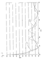
- the optical reflectivity R (in percent) is shown as a function of the wavelength 1 (in nm) of the light passing through the coated plastic substrate 10.
- the two lines H, L shown here refer to similar plastic substrates MR7 with a refractive index of 1.67 and an antireflective layer system consisting of SiN (refractive index 1.97, layer thickness 29 nm), SiO 2 (refractive index 1.47, layer thickness 26 nm). , SiN (refractive index 1.97, layer thickness 64 nm) and SiO 2 (refractive index 1.47, layer thickness 94 nm).
- the continuous line H results from a reflectivity measurement of a plastic substrate 10 coated using the method according to the invention, in which a 60 nm thick transition layer 14 (refractive index 1.56) with the adhesion promoter 16 and above for the suppression of undesired interference phenomena on the plastic substrate 10 first Matching layer of SiO 2 (layer thickness 15 nm, refractive index 1.47) and a second matching layer of SiN (layer thickness 2 nm, refractive index 1.97) were applied. Above these matching layers, in front of the actual antireflection layer, there is still a hard layer 18 of SiO 2 (layer thickness 740 nm, refractive index 1.47).
- a plastic substrate 10 was measured, in which a 3000 nm thick resist layer (refractive index 1.47) in a conventional coating method below the same, above specified antireflection coating was applied.
- the reflectivity R of the plastic substrate 10 coated in accordance with the invention (line H) oscillates significantly less than the reflectivity R of the plastic substrate 10 provided with the paint layer (line L). This shows the successful suppression of undesired interference phenomena manifesting themselves as oscillations in the reflectivity R by means of the adaptation layers.
- the hard layer 18 may also be applied by a so-called UV spin coating method.
- the hard layer 18 forming UV coatings are, for example, paints with the trade designation HT 850 and SHC 178.
- the refractive indices of the adhesion promoter 16 and formed from the UV coating hard layer 18 are advantageously coordinated so that unwanted interference (for example so-called Newtonian rings) are minimized. This is achieved by selecting the refractive index of the bonding agent 16 greater than that of the hard layer 18.
- the refractive index n of the adhesion promoter 16 is smaller than that of the plastic substrate 10, so that the following applies: n (substrate)> n (adhesion promoter)> n (hard layer).
- the layer thickness of the adhesion promoter 16 should be less than 200 nm.
- the thickness of the hard layer 18 is greater than that of the adhesion promoter 16 and is in particular between 500 nm and 5000 nm.
- the optical reflectivity R (in percent) as a function of Wavelength 1 (in nm) of the light passing through the coated plastic substrate 10 is shown.
- the two lines H1, L1 shown here refer to similar plastic substrates MR8 with a refractive index of 1.6.
- the continuous line H1 results from a reflectivity measurement of a plastic substrate 10 coated using the method according to the invention, in which the plastic substrate 10 initially has an 80 nm thick transition layer (refractive index of 1.55) with the adhesion promoter 16, above this a hard layer 18 (for example from the U.V.
- a plastic substrate 10 was measured, in which a 3000 nm thick resist layer (refractive index 1.47) was applied in a conventional coating method below the same, above-specified antireflection coating.
- the reflectivity R of the invention coated according to the plastic substrate 10 (line H1) oscillates significantly less than the reflectivity R of the reference plastic substrate 10 provided with the resist layer (line L1). This shows the successful suppression of undesired interference phenomena manifesting themselves as oscillations in the reflectivity R by means of the combination of specifically adapted and matched layers of adhesion promoter 16, hard layer 18 and sputtering layers.
- the layer thicknesses and arrangements of adaptation or subsequent functional layers can be calculated and optimized taking into account the refractive indices before application. This proves to be feasible and extremely advantageous in practice for the coatings produced by the process according to the invention because of the small layer thickness of the transition layer 14 of preferably less than 300 nm.
- the thickness of the lacquer layer is practically not possible or useful.
- the method according to the invention for producing such a coating is particularly cost-efficient, time-saving, precise and enables coatings of high optical quality.
- a reflectivity R of the continuous line H averaged over corresponding spectral ranges (for example 550 nm to 650 nm) has a lower value than that of the dashed line L.
- This behavior caused by the method according to the invention for the line H is particularly advantageous, especially with antireflection coatings.
- FIG. 4 another embodiment is shown.
- the optical reflectivity R (in percent) as a function of the wavelength 1 (in nm) of the light passing through the coated plastic substrate 10 is shown for an optical functional layer system 20 in the form of an antireflection layer.
- sputtered layers are inserted for plastic substrates 10 having a refractive index of 1.67 and higher for refractive index matching between primer 16 and hardcoat 18, the number, type, and thickness of the sputtering layers each to the combination of plastic substrate 10, primer 16, and hardcoat 18 to be adjusted.
- a possible example of such an embodiment is a plastic substrate 18 with a refractive index of 1.74, to which first an adhesion promoter 16 with a refractive index of 1.55 and a thickness of 40 nm, followed by two sputtered first sputtering layers consisting of SiO 2 (refractive index 1.47; Layer thickness 5 nm) and Si 3 N 4 (refractive index 1.97, layer thickness 6 nm), again followed by a hard layer 18 of a UV varnish (for example SHC 178 from Lens Technology International, La Mirada, CA 90638, USA) with a refractive index of 1.51 and a thickness of 1500 nm and finally five further sputtered second sputtering layers consisting of SiO 2 (refractive index 1.47, layer thickness 40 nm), Si 3 N 4 (refractive index 1.97, layer thickness 33 nm), SiO 2 (refractive index 1.47; Layer thickness 22 nm), Si 3 N 4 (refractive index 1.97, layer thickness 66 n
- an identical plastic substrate 10 was measured, in which no bonding agent 16 and no sputtering layers were applied before the hard layer 18, in this case the UV lacquer layer.
- the reflectivity R of the invention coated according to the plastic substrate 10 (line H2) oscillates significantly less than the reflectivity R of the reference substrate (line L2). This shows the successful suppression of unwanted oscillations as in the reflectivity R manifesting interference phenomena with the aid of the adapted combination of the layer of the adhesion promoter 16, the first sputtering layers, the hard layer 18 and the second sputtering layers.
- the method according to the invention will be described below with reference to FIG Fig. 5 illustrated device schemes with pointing in the process direction arrows detail.
- the plastic substrate 10 to be processed for example a spectacle lens formed from the MR8 plastic, is already mass-produced on its convex front side by means of dip coating and modified on its concave back in a custom-made by milling, grinding, polishing, etc., such that it meets the requirements optical effect on the lens properly met.
- this plastic substrate 10 is freed from any adhering impurities by means of a high-pressure cleaning device 24, in particular a high-pressure steam cleaning device.
- 0.1 ml to 5 ml, preferably 1 ml of a polymerizable liquid for forming the adhesion promoter 16, which forms the transition layer 14, is sprayed on in a spin-coating device (spin coating device) 26 on the concave rear side of the plastic substrate 10 to be coated.
- spin-coating device spin coating device
- the polymerizable liquid for forming the coupling agent 16 in the embodiments described above is a liquid of organic monomers, preferably based on acrylates or epoxies, for example the product P-201B from Lens Technology International, La Mirada, CA 90638, USA.
- the polymerisable liquid may preferably be polymerized under the irradiation of light, in particular ultraviolet (UV) light, that is to say light having substantial energy fractions in the ultraviolet part of its spectrum.
- UV ultraviolet
- the polymerization by the irradiation with ultraviolet light is in the UV irradiation device 28, to which the plastic substrates are preferably automated means not shown transporting carried.
- the UV irradiation device 28 has a UV radiation source, preferably a UV lamp.
- the polymer substrate-coated plastic substrate 10 is heated for a time of 0.1 second to 60 seconds, preferably about 10 seconds, at a light intensity of 1 W / cm 2 to 200 W / cm 2 , preferably about 100 W / cm 2 irradiated with ultraviolet light.
- these irradiation parameters such as the overall polymerization conditions, are to be adapted to the polymerizable liquid, the particular plastic substrate 10 and the desired properties of the transition layer 14.
- the convex front side of the plastic substrate 10 coated with the transition layer 14, which may be contaminated by a holding mechanism in the spin coating device 26, is cleaned by means of another high pressure cleaning device 25, preferably a high pressure steam cleaning device.
- This process step is optional and may, if appropriate, also take place at a different point in time in the production process or even be omitted altogether.
- the plastic substrate 10 can then be dried in a water removal device, for example in a continuous infrared oven.
- the optical functional layer system 20 is then applied in a coating device 32 to the thus conditioned transition layer 14 of the plastic substrate 10.
- the coating For example, to build the in Fig. 1 shown optical functional layer system 20 by means of sputtering or CVD coating method, in particular one in the EP-A-1 275 751 or EP-A-1 655 385 disclosed methods.
- the layer thicknesses of the individual layers of the optical functional layer system 20 can be adapted to the specific refractive index of the plastic substrate 10 or to other functional or application requirements in order to give the coating optimum optical properties.
- the coating is preferably carried out not only on the concave rear side provided with the transition layer 14, but likewise and optionally also simultaneously on the convex front side of the plastic substrate 10 hardened, for example, with a dip paint.
- the process which takes place in an automated form, preferably computer-assisted, is in particular for the coating of plastic glasses for spectacles or watches, but also suitable for optical elements of scientific instrumentation, packaging or energy technology.
Landscapes
- Chemical & Material Sciences (AREA)
- Health & Medical Sciences (AREA)
- General Chemical & Material Sciences (AREA)
- Chemical Kinetics & Catalysis (AREA)
- Medicinal Chemistry (AREA)
- Polymers & Plastics (AREA)
- Organic Chemistry (AREA)
- Physics & Mathematics (AREA)
- Engineering & Computer Science (AREA)
- Wood Science & Technology (AREA)
- Toxicology (AREA)
- Life Sciences & Earth Sciences (AREA)
- General Physics & Mathematics (AREA)
- Optics & Photonics (AREA)
- Surface Treatment Of Optical Elements (AREA)
- Application Of Or Painting With Fluid Materials (AREA)
Claims (20)
- Procédé pour le revêtement d'un substrat en matériau synthétique (10), dans lequel une couche de transition (14) qui sert en particulier à une adhérence améliorée d'une couche ou, selon le cas, d'un système de couches à appliquer sur celle-ci sur le substrat en matériau synthétique (10), est appliquée sur le substrat en matériau synthétique (10), un liquide polymérisable étant appliqué sur une surface (12) du substrat en matériau synthétique (10) à revêtir et y polymérisant en un promoteur d'adhérence (16) formant la couche de transition (14), caractérisé en ce qu'une couche dure (18) est appliquée sur la couche de transition (14) et l'indice de réfraction du promoteur d'adhérence (16) est choisi supérieur à l'indice de réfraction de la couche dure (18) et inférieur à l'indice de réfraction du substrat en matériau synthétique (10).
- Procédé selon la revendication 1, caractérisé en ce que le liquide polymérisable est réparti par revêtement à la tournette régulièrement à la surface (12) du substrat.
- Procédé selon la revendication 2, caractérisé en ce qu'on applique, lors du revêtement à la tournette, 0,5 ml à 5,0 ml, de préférence 1,0 ml du liquide polymérisable pour la formation du promoteur d'adhérence (16) sur la surface (12) du substrat et le substrat en matériau synthétique (10) est ensuite mis en rotation à une vitesse de rotation de 200 t/min à 2000 t/min, de préférence de 500 t/min, autour d'un axe de rotation orienté de manière essentiellement perpendiculaire à la surface (12) du substrat et passant de préférence au moins approximativement par le centre de masse du substrat en matériau synthétique (10).
- Procédé selon l'une quelconque des revendications 1 à 3, caractérisé en ce que la polymérisation du liquide polymérisable pour la formation du promoteur d'adhérence (16) est provoquée par la lumière, de préférence de la lumière ultraviolette (UV).
- Procédé selon la revendication 4, caractérisé en ce que la polymérisation sous lumière ultraviolette (UV) est réalisée par une source de rayonnement UV, de préférence une lampe UV, à un temps d'irradiation de 0,1 s à 60 s, de préférence d'environ 10 s à une intensité lumineuse de 1 W/cm2 à 200 W/cm2, de préférence de 100 W/cm2.
- Procédé selon l'une quelconque des revendications 1 à 5, caractérisé en ce que l'épaisseur de la couche de promoteur d'adhérence (16) est de 10 nm à 5000 nm, de préférence de 40 nm à 200 nm, de manière particulièrement préférée de 60 nm à 100 nm.
- Procédé selon l'une quelconque des revendications 1 à 6, caractérisé en ce que des phénomènes d'interférence optique non souhaités sont supprimés par une adaptation déterminée au préalable par calcul des épaisseurs de couche du système de couches à appliquer au-dessus de la couche de transition (14), en particulier d'un système de couches d'adaptation.
- Procédé selon l'une quelconque des revendications 1 à 7, caractérisé en ce que la surface de substrat (12) à revêtir est nettoyée avant l'application de la couche de transition (14) par nettoyage à la vapeur sous haute pression.
- Procédé selon l'une quelconque des revendications 1 à 8, caractérisé en ce qu'au moins une couche pulvérisée appliquée par pulvérisation est réalisée entre la couche de transition (14) en promoteur d'adhérence (16) et la couche dure (18).
- Procédé selon l'une quelconque des revendications 1 à 9, caractérisé en ce que la couche ou, selon le cas, le système de couches, qui est appliqué(e) au-dessus de la couche de transition (14) présente un système de couches fonctionnel optique (20) avec une couche antiréfléchissante servant à l'antireflet.
- Procédé selon l'une quelconque des revendications 1 à 10, caractérisé en ce que la couche ou, selon le cas, le système de couches qui est appliqué(e) au-dessus de la couche de transition (14) présente une couche de finition (22) hydrophobe.
- Procédé selon l'une quelconque des revendications 1 à 11, caractérisé en ce que la couche ou, selon le cas, le système de couches au-dessus de la couche de transition (14) est appliquée par pulvérisation, vaporisation chimique (CVD), pulvérisation soutenue par CVD, de préférence par pulvérisation ou par revêtement à la tournette aux UV.
- Procédé selon l'une quelconque des revendications 1 à 12, caractérisé en ce que l'épaisseur de la couche dure (18) est supérieure à l'épaisseur de couche du promoteur d'adhérence (16) et est de 500 nm à 5000 nm.
- Procédé selon l'une quelconque des revendications 1 à 13, caractérisé en ce que la couche dure (18) est appliquée par un procédé de revêtement à la tournette aux UV.
- Dispositif pour la réalisation du procédé selon l'une quelconque des revendications 1 à 14, qui présente un dispositif de nettoyage à haute pression (24), un dispositif de revêtement à la tournette (26), un dispositif d'irradiation aux UV (28) et un dispositif de revêtement (32), qui sont prévus pour être traversés dans l'ordre mentionné par le substrat en matériau synthétique (10).
- Dispositif selon la revendication 15, caractérisé en ce qu'il est exploité de manière au moins partiellement automatisée, de préférence complètement automatisée et le procédé de production est de préférence contrôlé par un ordinateur.
- Dispositif selon les revendications 15 ou 16, caractérisé en ce que le dispositif de revêtement (32) est prévu pour le revêtement par pulvérisation, vaporisation chimique (CVD) ou pulvérisation soutenue par CVD, de préférence par pulvérisation.
- Dispositif selon l'une quelconque des revendications 15 ou 17, caractérisé en ce que le dispositif de revêtement (32) ou un autre dispositif de revêtement (34) appartenant au dispositif est prévu pour l'application d'une couche de finition (22) hydrophobe.
- Revêtement réalisé selon un procédé selon l'une quelconque des revendications 1 à 14.
- Revêtement selon la revendication 19, caractérisé en ce que la couche de transition (14) présente une épaisseur de couche inférieure à 500 nm, de préférence inférieure à 300 nm, de manière telle que des phénomènes d'interférence optiques non souhaités sont supprimés par le système de couches à appliquer au-dessus de la couche de transition (14), en particulier le système de couches d'adaptation ou le système de couches fonctionnelles optiques (20), présentant des épaisseurs de couches optimisées par calcul.
Applications Claiming Priority (2)
| Application Number | Priority Date | Filing Date | Title |
|---|---|---|---|
| CH1802007 | 2007-02-02 | ||
| PCT/CH2008/000028 WO2008092288A1 (fr) | 2007-02-02 | 2008-01-29 | Procédé de revêtement d'un substrat en matière plastique optique |
Publications (3)
| Publication Number | Publication Date |
|---|---|
| EP2125251A1 EP2125251A1 (fr) | 2009-12-02 |
| EP2125251B1 true EP2125251B1 (fr) | 2011-11-23 |
| EP2125251B8 EP2125251B8 (fr) | 2012-03-14 |
Family
ID=39247320
Family Applications (1)
| Application Number | Title | Priority Date | Filing Date |
|---|---|---|---|
| EP08700533A Active EP2125251B8 (fr) | 2007-02-02 | 2008-01-29 | Procédé de revêtement d'un substrat en matière plastique optique |
Country Status (4)
| Country | Link |
|---|---|
| US (1) | US20100003509A1 (fr) |
| EP (1) | EP2125251B8 (fr) |
| AT (1) | ATE534472T1 (fr) |
| WO (1) | WO2008092288A1 (fr) |
Families Citing this family (2)
| Publication number | Priority date | Publication date | Assignee | Title |
|---|---|---|---|---|
| CN108300977A (zh) * | 2018-04-12 | 2018-07-20 | 广东振华科技股份有限公司 | 一种适用于柔性基材的光学薄膜及其制作方法 |
| DE102019131521A1 (de) * | 2019-11-21 | 2021-05-27 | Rehau Ag + Co | Verfahren zum Beschichten eines Kunststoffbauteils und Kunststoffbauteil |
Family Cites Families (12)
| Publication number | Priority date | Publication date | Assignee | Title |
|---|---|---|---|---|
| US4218508A (en) * | 1978-04-12 | 1980-08-19 | General Electric Company | Polycarbonate articles coated with an adherent, durable silica filled organopolysiloxane coating and process for producing same |
| US4200681A (en) * | 1978-11-13 | 1980-04-29 | General Electric Company | Glass coated polycarbonate articles |
| JPH0642002B2 (ja) * | 1983-07-29 | 1994-06-01 | セイコーエプソン株式会社 | プラスチックレンズ |
| US4842941A (en) * | 1987-04-06 | 1989-06-27 | General Electric Company | Method for forming abrasion-resistant polycarbonate articles, and articles of manufacture produced thereby |
| US5496641A (en) * | 1991-06-13 | 1996-03-05 | Nippon Sheet Glass Co., Ltd. | Plastic lens |
| US5316791A (en) * | 1993-01-21 | 1994-05-31 | Sdc Coatings Inc. | Process for improving impact resistance of coated plastic substrates |
| US5846649A (en) * | 1994-03-03 | 1998-12-08 | Monsanto Company | Highly durable and abrasion-resistant dielectric coatings for lenses |
| US5525451A (en) * | 1995-05-30 | 1996-06-11 | Xerox Corporation | Photoreceptor fabrication method |
| US6376064B1 (en) * | 1999-12-13 | 2002-04-23 | General Electric Company | Layered article with improved microcrack resistance and method of making |
| WO2004011158A1 (fr) * | 2002-07-31 | 2004-02-05 | Vision-Ease Lens, Inc. | Application par centrifugation de revetements reticules par voie thermique |
| DE102005059485B4 (de) * | 2005-02-11 | 2012-08-02 | Carl Zeiss Vision Gmbh | Verfahren zum Beschichten von Gegenständen aus Kunststoff |
| EP1864181B1 (fr) * | 2005-03-01 | 2016-08-03 | Carl Zeiss Vision Australia Holdings Ltd. | Revêtements pour éléments de lentilles ophtalmiques |
-
2008
- 2008-01-29 AT AT08700533T patent/ATE534472T1/de active
- 2008-01-29 WO PCT/CH2008/000028 patent/WO2008092288A1/fr not_active Ceased
- 2008-01-29 US US12/449,336 patent/US20100003509A1/en not_active Abandoned
- 2008-01-29 EP EP08700533A patent/EP2125251B8/fr active Active
Also Published As
| Publication number | Publication date |
|---|---|
| EP2125251A1 (fr) | 2009-12-02 |
| US20100003509A1 (en) | 2010-01-07 |
| ATE534472T1 (de) | 2011-12-15 |
| WO2008092288A1 (fr) | 2008-08-07 |
| EP2125251B8 (fr) | 2012-03-14 |
Similar Documents
| Publication | Publication Date | Title |
|---|---|---|
| EP2274641B1 (fr) | Procédé pour la fabrication d'un système de couches d'interférence diminuant la réflexion | |
| DE60308473T2 (de) | Optisches Element mit Antireflexfilm | |
| DE19912737A1 (de) | Verfahren zur Herstellung von porösen SiO¶x¶-Schichten und poröse SiO¶x¶-Schichten | |
| DE2751221A1 (de) | Verfahren zur aufbringung eines reflexionsvermindernden belages auf unterlagen aus organischem material | |
| DE602004010491T2 (de) | Polarisierender kratzfester optischer Film und Herstellungsverfahren hierfür | |
| WO2009074146A2 (fr) | Procédé de réalisation d'une couche réduisant la réflexion et élément optique pourvu d'une couche réduisant la réflexion | |
| EP1307767B1 (fr) | Revetement reduisant la reflexion | |
| EP2125251B1 (fr) | Procédé de revêtement d'un substrat en matière plastique optique | |
| EP1407059B1 (fr) | Procede et dispositif de production d'un systeme multicouche d'action optique | |
| WO2024200671A1 (fr) | Procédé de fabrication d'empilements de substrats pour le traitement ultérieur de verres composites d'éléments optiques | |
| DE102012008640A1 (de) | Verfahren zur Herstellung eines optischen Moduls mit einer Polymeroptik | |
| DE19834314A1 (de) | Verfahren zum Aufbringen einer Kratzschutzschicht und eines Entspiegelungsschichtsystems und Vorrichtung zu seiner Durchführung | |
| CH690511A5 (de) | Optisches Bauteil und Verfahren zum Herstellen eines solchen. | |
| EP1417042A2 (fr) | Procede de production d'un corps synthetique revetu | |
| DE102013211233A1 (de) | Optische Bauelemente und Verfahren zu deren Herstellung | |
| EP0038281A2 (fr) | Procédé de modification des propriétés de réflexion de surfaces | |
| EP2369032B1 (fr) | Procédé de fabrication de surfaces colorées | |
| WO2010048975A1 (fr) | Revêtement d'oxyde d'hafnium | |
| EP3152606B1 (fr) | Revêtement des faces d'extrémité d'un guide d'onde | |
| DE19838826B4 (de) | Optisches Element mit transparenter, kratzfester Beschichtung, Verfahren und Vorrichtung zu seiner Herstellung sowie dessen Verwendung | |
| EP1164388A2 (fr) | Article avec des couches optiques | |
| EP1245298A1 (fr) | Procédé de fabrication de pièces en plastiques revêtues | |
| DE102015116121A1 (de) | Optisches Bauteil und Verfahren zum Beschichten eines Optischen Bauteils | |
| DE102018105859A1 (de) | Reflexionsminderndes Schichtsystem und Verfahren zu dessen Herstellung | |
| DE102011119931B4 (de) | Verfahren zur Bearbeitung eines präzisionsoptischen Bauteiles, präzisionsoptisches Bauteil und Verwendung eines thermischen Nachbehandlungsverfahrens zur planmäßigen Einstellung der Schichtspannung einer Beschichtung eines präzisionsoptischen Bauteiles |
Legal Events
| Date | Code | Title | Description |
|---|---|---|---|
| PUAI | Public reference made under article 153(3) epc to a published international application that has entered the european phase |
Free format text: ORIGINAL CODE: 0009012 |
|
| 17P | Request for examination filed |
Effective date: 20090612 |
|
| AK | Designated contracting states |
Kind code of ref document: A1 Designated state(s): AT BE BG CH CY CZ DE DK EE ES FI FR GB GR HR HU IE IS IT LI LT LU LV MC MT NL NO PL PT RO SE SI SK TR |
|
| DAX | Request for extension of the european patent (deleted) | ||
| 17Q | First examination report despatched |
Effective date: 20100412 |
|
| GRAP | Despatch of communication of intention to grant a patent |
Free format text: ORIGINAL CODE: EPIDOSNIGR1 |
|
| GRAS | Grant fee paid |
Free format text: ORIGINAL CODE: EPIDOSNIGR3 |
|
| GRAA | (expected) grant |
Free format text: ORIGINAL CODE: 0009210 |
|
| AK | Designated contracting states |
Kind code of ref document: B1 Designated state(s): AT BE BG CH CY CZ DE DK EE ES FI FR GB GR HR HU IE IS IT LI LT LU LV MC MT NL NO PL PT RO SE SI SK TR |
|
| REG | Reference to a national code |
Ref country code: GB Ref legal event code: FG4D Free format text: NOT ENGLISH |
|
| REG | Reference to a national code |
Ref country code: CH Ref legal event code: NV Representative=s name: PATENTANWAELTE SCHAAD, BALASS, MENZL & PARTNER AG Ref country code: CH Ref legal event code: EP |
|
| REG | Reference to a national code |
Ref country code: IE Ref legal event code: FG4D Free format text: LANGUAGE OF EP DOCUMENT: GERMAN |
|
| REG | Reference to a national code |
Ref country code: DE Ref legal event code: R096 Ref document number: 502008005662 Country of ref document: DE Effective date: 20120119 |
|
| REG | Reference to a national code |
Ref country code: DE Ref legal event code: R082 Ref document number: 502008005662 Country of ref document: DE Representative=s name: BITTERICH, DR. KELLER, SCHWERTFEGER, DE Ref country code: DE Ref legal event code: R082 Ref document number: 502008005662 Country of ref document: DE Representative=s name: PATENTANWAELTE DR. KELLER, SCHWERTFEGER, DE |
|
| REG | Reference to a national code |
Ref country code: NL Ref legal event code: VDEP Effective date: 20111123 |
|
| LTIE | Lt: invalidation of european patent or patent extension |
Effective date: 20111123 |
|
| PG25 | Lapsed in a contracting state [announced via postgrant information from national office to epo] |
Ref country code: IS Free format text: LAPSE BECAUSE OF FAILURE TO SUBMIT A TRANSLATION OF THE DESCRIPTION OR TO PAY THE FEE WITHIN THE PRESCRIBED TIME-LIMIT Effective date: 20120323 Ref country code: LT Free format text: LAPSE BECAUSE OF FAILURE TO SUBMIT A TRANSLATION OF THE DESCRIPTION OR TO PAY THE FEE WITHIN THE PRESCRIBED TIME-LIMIT Effective date: 20111123 Ref country code: NO Free format text: LAPSE BECAUSE OF FAILURE TO SUBMIT A TRANSLATION OF THE DESCRIPTION OR TO PAY THE FEE WITHIN THE PRESCRIBED TIME-LIMIT Effective date: 20120223 |
|
| PG25 | Lapsed in a contracting state [announced via postgrant information from national office to epo] |
Ref country code: NL Free format text: LAPSE BECAUSE OF FAILURE TO SUBMIT A TRANSLATION OF THE DESCRIPTION OR TO PAY THE FEE WITHIN THE PRESCRIBED TIME-LIMIT Effective date: 20111123 Ref country code: GR Free format text: LAPSE BECAUSE OF FAILURE TO SUBMIT A TRANSLATION OF THE DESCRIPTION OR TO PAY THE FEE WITHIN THE PRESCRIBED TIME-LIMIT Effective date: 20120224 Ref country code: HR Free format text: LAPSE BECAUSE OF FAILURE TO SUBMIT A TRANSLATION OF THE DESCRIPTION OR TO PAY THE FEE WITHIN THE PRESCRIBED TIME-LIMIT Effective date: 20111123 Ref country code: SE Free format text: LAPSE BECAUSE OF FAILURE TO SUBMIT A TRANSLATION OF THE DESCRIPTION OR TO PAY THE FEE WITHIN THE PRESCRIBED TIME-LIMIT Effective date: 20111123 Ref country code: PT Free format text: LAPSE BECAUSE OF FAILURE TO SUBMIT A TRANSLATION OF THE DESCRIPTION OR TO PAY THE FEE WITHIN THE PRESCRIBED TIME-LIMIT Effective date: 20120323 Ref country code: SI Free format text: LAPSE BECAUSE OF FAILURE TO SUBMIT A TRANSLATION OF THE DESCRIPTION OR TO PAY THE FEE WITHIN THE PRESCRIBED TIME-LIMIT Effective date: 20111123 Ref country code: LV Free format text: LAPSE BECAUSE OF FAILURE TO SUBMIT A TRANSLATION OF THE DESCRIPTION OR TO PAY THE FEE WITHIN THE PRESCRIBED TIME-LIMIT Effective date: 20111123 |
|
| REG | Reference to a national code |
Ref country code: IE Ref legal event code: FD4D |
|
| PG25 | Lapsed in a contracting state [announced via postgrant information from national office to epo] |
Ref country code: CY Free format text: LAPSE BECAUSE OF FAILURE TO SUBMIT A TRANSLATION OF THE DESCRIPTION OR TO PAY THE FEE WITHIN THE PRESCRIBED TIME-LIMIT Effective date: 20111123 |
|
| BERE | Be: lapsed |
Owner name: SATISLOH PHOTONICS A.G. Effective date: 20120131 |
|
| PG25 | Lapsed in a contracting state [announced via postgrant information from national office to epo] |
Ref country code: SK Free format text: LAPSE BECAUSE OF FAILURE TO SUBMIT A TRANSLATION OF THE DESCRIPTION OR TO PAY THE FEE WITHIN THE PRESCRIBED TIME-LIMIT Effective date: 20111123 Ref country code: CZ Free format text: LAPSE BECAUSE OF FAILURE TO SUBMIT A TRANSLATION OF THE DESCRIPTION OR TO PAY THE FEE WITHIN THE PRESCRIBED TIME-LIMIT Effective date: 20111123 Ref country code: DK Free format text: LAPSE BECAUSE OF FAILURE TO SUBMIT A TRANSLATION OF THE DESCRIPTION OR TO PAY THE FEE WITHIN THE PRESCRIBED TIME-LIMIT Effective date: 20111123 Ref country code: IE Free format text: LAPSE BECAUSE OF FAILURE TO SUBMIT A TRANSLATION OF THE DESCRIPTION OR TO PAY THE FEE WITHIN THE PRESCRIBED TIME-LIMIT Effective date: 20111123 Ref country code: BG Free format text: LAPSE BECAUSE OF FAILURE TO SUBMIT A TRANSLATION OF THE DESCRIPTION OR TO PAY THE FEE WITHIN THE PRESCRIBED TIME-LIMIT Effective date: 20120223 Ref country code: EE Free format text: LAPSE BECAUSE OF FAILURE TO SUBMIT A TRANSLATION OF THE DESCRIPTION OR TO PAY THE FEE WITHIN THE PRESCRIBED TIME-LIMIT Effective date: 20111123 |
|
| PG25 | Lapsed in a contracting state [announced via postgrant information from national office to epo] |
Ref country code: MC Free format text: LAPSE BECAUSE OF NON-PAYMENT OF DUE FEES Effective date: 20120131 Ref country code: PL Free format text: LAPSE BECAUSE OF FAILURE TO SUBMIT A TRANSLATION OF THE DESCRIPTION OR TO PAY THE FEE WITHIN THE PRESCRIBED TIME-LIMIT Effective date: 20111123 Ref country code: RO Free format text: LAPSE BECAUSE OF FAILURE TO SUBMIT A TRANSLATION OF THE DESCRIPTION OR TO PAY THE FEE WITHIN THE PRESCRIBED TIME-LIMIT Effective date: 20111123 |
|
| PLBE | No opposition filed within time limit |
Free format text: ORIGINAL CODE: 0009261 |
|
| STAA | Information on the status of an ep patent application or granted ep patent |
Free format text: STATUS: NO OPPOSITION FILED WITHIN TIME LIMIT |
|
| 26N | No opposition filed |
Effective date: 20120824 |
|
| REG | Reference to a national code |
Ref country code: DE Ref legal event code: R097 Ref document number: 502008005662 Country of ref document: DE Effective date: 20120824 |
|
| PG25 | Lapsed in a contracting state [announced via postgrant information from national office to epo] |
Ref country code: BE Free format text: LAPSE BECAUSE OF NON-PAYMENT OF DUE FEES Effective date: 20120131 |
|
| PG25 | Lapsed in a contracting state [announced via postgrant information from national office to epo] |
Ref country code: ES Free format text: LAPSE BECAUSE OF FAILURE TO SUBMIT A TRANSLATION OF THE DESCRIPTION OR TO PAY THE FEE WITHIN THE PRESCRIBED TIME-LIMIT Effective date: 20120305 |
|
| PG25 | Lapsed in a contracting state [announced via postgrant information from national office to epo] |
Ref country code: FI Free format text: LAPSE BECAUSE OF FAILURE TO SUBMIT A TRANSLATION OF THE DESCRIPTION OR TO PAY THE FEE WITHIN THE PRESCRIBED TIME-LIMIT Effective date: 20111123 |
|
| PG25 | Lapsed in a contracting state [announced via postgrant information from national office to epo] |
Ref country code: MT Free format text: LAPSE BECAUSE OF FAILURE TO SUBMIT A TRANSLATION OF THE DESCRIPTION OR TO PAY THE FEE WITHIN THE PRESCRIBED TIME-LIMIT Effective date: 20111123 |
|
| REG | Reference to a national code |
Ref country code: AT Ref legal event code: MM01 Ref document number: 534472 Country of ref document: AT Kind code of ref document: T Effective date: 20130129 |
|
| PG25 | Lapsed in a contracting state [announced via postgrant information from national office to epo] |
Ref country code: TR Free format text: LAPSE BECAUSE OF FAILURE TO SUBMIT A TRANSLATION OF THE DESCRIPTION OR TO PAY THE FEE WITHIN THE PRESCRIBED TIME-LIMIT Effective date: 20111123 |
|
| PG25 | Lapsed in a contracting state [announced via postgrant information from national office to epo] |
Ref country code: AT Free format text: LAPSE BECAUSE OF NON-PAYMENT OF DUE FEES Effective date: 20130129 Ref country code: LU Free format text: LAPSE BECAUSE OF NON-PAYMENT OF DUE FEES Effective date: 20120129 |
|
| PG25 | Lapsed in a contracting state [announced via postgrant information from national office to epo] |
Ref country code: HU Free format text: LAPSE BECAUSE OF FAILURE TO SUBMIT A TRANSLATION OF THE DESCRIPTION OR TO PAY THE FEE WITHIN THE PRESCRIBED TIME-LIMIT Effective date: 20080129 |
|
| REG | Reference to a national code |
Ref country code: FR Ref legal event code: PLFP Year of fee payment: 9 |
|
| REG | Reference to a national code |
Ref country code: FR Ref legal event code: PLFP Year of fee payment: 10 |
|
| REG | Reference to a national code |
Ref country code: FR Ref legal event code: PLFP Year of fee payment: 11 |
|
| P01 | Opt-out of the competence of the unified patent court (upc) registered |
Effective date: 20230525 |
|
| REG | Reference to a national code |
Ref country code: CH Ref legal event code: U11 Free format text: ST27 STATUS EVENT CODE: U-0-0-U10-U11 (AS PROVIDED BY THE NATIONAL OFFICE) Effective date: 20260201 |
|
| PGFP | Annual fee paid to national office [announced via postgrant information from national office to epo] |
Ref country code: GB Payment date: 20260127 Year of fee payment: 19 |
|
| PGFP | Annual fee paid to national office [announced via postgrant information from national office to epo] |
Ref country code: DE Payment date: 20260128 Year of fee payment: 19 |
|
| PGFP | Annual fee paid to national office [announced via postgrant information from national office to epo] |
Ref country code: IT Payment date: 20260121 Year of fee payment: 19 |
|
| PGFP | Annual fee paid to national office [announced via postgrant information from national office to epo] |
Ref country code: FR Payment date: 20260126 Year of fee payment: 19 |
|
| PGFP | Annual fee paid to national office [announced via postgrant information from national office to epo] |
Ref country code: CH Payment date: 20260201 Year of fee payment: 19 |