EP2128603A1 - Procédé pour déterminer une propriété optique d'une couche optique - Google Patents
Procédé pour déterminer une propriété optique d'une couche optique Download PDFInfo
- Publication number
- EP2128603A1 EP2128603A1 EP08009845A EP08009845A EP2128603A1 EP 2128603 A1 EP2128603 A1 EP 2128603A1 EP 08009845 A EP08009845 A EP 08009845A EP 08009845 A EP08009845 A EP 08009845A EP 2128603 A1 EP2128603 A1 EP 2128603A1
- Authority
- EP
- European Patent Office
- Prior art keywords
- reflection
- transmission
- value
- spectrum
- optical
- Prior art date
- Legal status (The legal status is an assumption and is not a legal conclusion. Google has not performed a legal analysis and makes no representation as to the accuracy of the status listed.)
- Withdrawn
Links
- 230000003287 optical effect Effects 0.000 title claims abstract description 109
- 238000000034 method Methods 0.000 title claims abstract description 35
- 230000005540 biological transmission Effects 0.000 claims abstract description 41
- 238000000411 transmission spectrum Methods 0.000 claims abstract description 27
- 238000001228 spectrum Methods 0.000 claims abstract description 26
- 230000003595 spectral effect Effects 0.000 claims description 33
- 238000009826 distribution Methods 0.000 claims description 16
- 238000010521 absorption reaction Methods 0.000 claims description 14
- 238000005457 optimization Methods 0.000 claims description 10
- 238000004590 computer program Methods 0.000 claims description 7
- 230000008033 biological extinction Effects 0.000 claims description 6
- 238000011156 evaluation Methods 0.000 claims description 6
- 238000001514 detection method Methods 0.000 claims description 5
- 238000005375 photometry Methods 0.000 claims description 3
- 238000005259 measurement Methods 0.000 description 44
- 238000004458 analytical method Methods 0.000 description 11
- 230000006870 function Effects 0.000 description 9
- 238000012545 processing Methods 0.000 description 9
- 238000000576 coating method Methods 0.000 description 5
- XUIMIQQOPSSXEZ-UHFFFAOYSA-N Silicon Chemical compound [Si] XUIMIQQOPSSXEZ-UHFFFAOYSA-N 0.000 description 2
- 229910021417 amorphous silicon Inorganic materials 0.000 description 2
- 239000011521 glass Substances 0.000 description 2
- 229910021424 microcrystalline silicon Inorganic materials 0.000 description 2
- 239000000203 mixture Substances 0.000 description 2
- 229910052710 silicon Inorganic materials 0.000 description 2
- 239000010703 silicon Substances 0.000 description 2
- 238000001069 Raman spectroscopy Methods 0.000 description 1
- 238000000862 absorption spectrum Methods 0.000 description 1
- 239000013078 crystal Substances 0.000 description 1
- 230000001419 dependent effect Effects 0.000 description 1
- 238000006073 displacement reaction Methods 0.000 description 1
- 230000002068 genetic effect Effects 0.000 description 1
- 238000004519 manufacturing process Methods 0.000 description 1
- 239000000463 material Substances 0.000 description 1
- 235000019988 mead Nutrition 0.000 description 1
- 239000000758 substrate Substances 0.000 description 1
- 238000012360 testing method Methods 0.000 description 1
Images


Classifications
-
- G—PHYSICS
- G01—MEASURING; TESTING
- G01N—INVESTIGATING OR ANALYSING MATERIALS BY DETERMINING THEIR CHEMICAL OR PHYSICAL PROPERTIES
- G01N21/00—Investigating or analysing materials by the use of optical means, i.e. using sub-millimetre waves, infrared, visible or ultraviolet light
- G01N21/84—Systems specially adapted for particular applications
- G01N21/8422—Investigating thin films, e.g. matrix isolation method
-
- G—PHYSICS
- G01—MEASURING; TESTING
- G01B—MEASURING LENGTH, THICKNESS OR SIMILAR LINEAR DIMENSIONS; MEASURING ANGLES; MEASURING AREAS; MEASURING IRREGULARITIES OF SURFACES OR CONTOURS
- G01B11/00—Measuring arrangements characterised by the use of optical techniques
- G01B11/02—Measuring arrangements characterised by the use of optical techniques for measuring length, width or thickness
- G01B11/06—Measuring arrangements characterised by the use of optical techniques for measuring length, width or thickness for measuring thickness ; e.g. of sheet material
-
- G—PHYSICS
- G01—MEASURING; TESTING
- G01B—MEASURING LENGTH, THICKNESS OR SIMILAR LINEAR DIMENSIONS; MEASURING ANGLES; MEASURING AREAS; MEASURING IRREGULARITIES OF SURFACES OR CONTOURS
- G01B11/00—Measuring arrangements characterised by the use of optical techniques
- G01B11/02—Measuring arrangements characterised by the use of optical techniques for measuring length, width or thickness
- G01B11/06—Measuring arrangements characterised by the use of optical techniques for measuring length, width or thickness for measuring thickness ; e.g. of sheet material
- G01B11/0616—Measuring arrangements characterised by the use of optical techniques for measuring length, width or thickness for measuring thickness ; e.g. of sheet material of coating
-
- G—PHYSICS
- G01—MEASURING; TESTING
- G01N—INVESTIGATING OR ANALYSING MATERIALS BY DETERMINING THEIR CHEMICAL OR PHYSICAL PROPERTIES
- G01N21/00—Investigating or analysing materials by the use of optical means, i.e. using sub-millimetre waves, infrared, visible or ultraviolet light
- G01N21/17—Systems in which incident light is modified in accordance with the properties of the material investigated
- G01N21/59—Transmissivity
Definitions
- the present invention relates to determining the thickness and optical properties of optical layers.
- Current solar cells are comprised of one or plural optical layers, whose optical properties significantly influence the possible energy generation.
- One of the optical layers is the absorption layer, which is often made of silicon (Si).
- Si silicon
- the energy band gap, or its position is a substantial parameter, since it determines which spectral ranges of the sunlight are absorbed, and which are not absorbed. In order to assure the required quality of large surface solar cells, the energy band gap and other absorption properties therefore have to comply with particular requirements with respect to the absorption spectra.
- the position of the energy of the band gap can be influenced e.g. by performing the coating process, which is used for forming the absorption layer, in a suitable manner. Said energy position particularly depends on the crystal structure of the silicon used, so that e.g. for thin layer solar cells, a mix ratio between an amorphous silicon and a microcrystalline silicon can be adjusted by means of one or plural coating process parameters, so that the energy position of the optical band gap corresponds to a target value.
- the mix ratio of amorphous and microcrystalline silicon can e.g. be determined by Raman-Spectroscopy.
- the spectral distribution of the refractory index n( ⁇ ) and of the extinction coefficient k( ⁇ ) can be determined e.g. from an optical measurement with an ellipsometer, wherein ⁇ characterizes the wavelength.
- the present invention is based on the finding that the optical models of the optical layers, which are used in the context of the known method for determining the energy band gap, like e.g. Tauc-Lorentz Model, can also be used for determining the energy band gap based on a spectral photometric measurement.
- the position of the energy band gap can e.g. be determined based on a measurement of a spectral transmission value T( ⁇ ) and of a spectral reflection value R( ⁇ ) using an optical model of an optical layer. If the model of the optical layer can e.g. parameterized thus by a change of one or several parameters e.g. the respective energy band gap can be determined, which can be associated with the respective transmission and/or reflection value and which most closely corresponds to the detected values.
- the optical property can e.g. be determined based on a minimization task using the model of the optical layer.
- a measuring system which measures in two dimension can be used to prove the optical homogeneity of large area coatings with a surface area of e.g. more than 1 m 2 .
- a measurement system of this type can e.g. determine the spectral transmission T( ⁇ ) and the spectral reflection R( ⁇ ) as well as additional layer properties, like e.g. the color spectrum or the energy position of transmission- and reflection-maxima and -minima.
- a measurement system of said type can also be used for determining the optical energy band gap, so that the measurements neither have to be performed with an ellipsometer, nor the transmission measurement has to be performed under the Brewster-angle. Instead e.g.
- a spectral photometer is used for measuring the transmission T( ⁇ ) and the reflection R( ⁇ ).
- the measurement data can be stored e.g. for any location that is being measured wherein e.g. a computer program reads in the spectral data for each location and feeds it to a suitable optical model, based on which e.g. the layer thickness d, the spectral distribution n( ⁇ ), the spectral distribution K( ⁇ ) and the optical energy band gap or its position are determined as optical properties.
- the detection of the optical property based on the optical model of the optical layer can e.g. be performed by means of a fit-software.
- the method according to the invention can e.g. be implemented through an expansion of a system, which measures in two dimensions for proofing the optical homogeneity of large area coatings, with a location resolved determination of the optical energy band gap as an additional parameter
- ellipsometers For determining the optical properties e.g. of solar absorption layers which are deposited on a large area, ellipsometers with large scanning tables can be used. However, it is disadvantageous that a measurement with an ellipsometer requires more time than a measurement with a spectral photometer. Furthermore, ellipsometers are more expensive than spectral photometers and they require a higher precision when adjusting a sample, which is time consuming and error prone.
- the invention relates to a method for determining an optical property of an optical layer including the detection of a transmission value or a transmission spectrum, and a reflection value or a reflection spectrum of the optical layer and for determining the optical property based on the transmission value or the transmission spectrum, the reflection value or the reflection spectrum and a model of the optical layer.
- the optical property is an energy band gap, or its position, or an absorption coefficient, or an extinction coefficient, or a refractory index, or a layer thickness.
- the transmission value or the transmission spectrum and/or the reflection value, or the reflection spectrum can be detected by a spectral-photometric measurement.
- the transmission value or the transmission spectrum and /or the reflection value or the reflection spectrum can be detected in a predetermined range of the optical layer.
- the transmission value or the transmission spectrum and the reflection value or the reflection spectrum can be detected in a predetermined portion of the optical layer, wherein an additional transmission value or an additional transmission spectrum an additional reflection value or an additional reflection spectrum are detected in an additional predetermined portion of the optical layer, wherein a distribution, in particular a local distribution of the optical property is determined based on the transmission values or the transmission spectra and the reflection values or the reflection spectra.
- the optical layer is a solar absorption layer.
- an optimization method is used for determining the optical property, in particular a non linear optimization method using the model of the optical layer.
- a theoretical reflection value or a theoretical reflection spectrum and a theoretical transmission value or a theoretical transmission spectrum are determined, wherein for determining the optical property a minimum of an evaluation function is determined, which is related to the model of the optical layer, using the theoretical reflection value or the theoretical reflection spectrum, the theoretical transmission value or the theoretical transmission spectrum, the detected reflection value or the detected reflection spectrum and the detected transmission value or the detected transmission spectrum.
- the model of the optical layer is a parameterizable optical model or an Urbach-model or a Tauc-model or a Tauc-Lorentz-model or a Foroui-Bloomer-model or a Dasgupta-model or an O'Leary-model or a Cody-Lorentz-model.
- the invention furthermore relates to a device for determining and optical property of an optical layer by a detection means, in particular a spectral photometer for detecting a transmission value or a transmission spectrum or reflection value or refraction spectrum of the optical layer and a processor for determining the optical property based on the transmission value or the transmission spectrum, the reflection value or a reflection spectrum and a model of the optical layer.
- a detection means in particular a spectral photometer for detecting a transmission value or a transmission spectrum or reflection value or refraction spectrum of the optical layer and a processor for determining the optical property based on the transmission value or the transmission spectrum, the reflection value or a reflection spectrum and a model of the optical layer.
- the program of the processor is configured to perform the method according to the invention.
- the method furthermore relates to a computer program for performing the method according to the invention, when the computer program is executed on a computer.
- the invention furthermore relates to a program driven device, which is configured to execute the computer program for performing the method according to the invention.
- a transmission and a reflection of the optical layer are detected in step 101, wherein said detection can be performed in parallel or in series.
- the optical property e.g. an energy band gap and/or an extinction coefficient and/or a refractory index and/or a layer thickness are determined based on the transmission, the reflection and on a model of the optical layer.
- the model of the optical layer is preferably an optical model, which can e.g. be characterized by an evaluation function, so that the optical property can be determined e.g. by the minimizing the evaluation function.
- the mathematical non linear optimization methods or optimization algorithms can be used, like e.g. the Simplex-method of Nelder and Mead, the Powell Algorithm or an optimization by a genetic algorithm.
- the non linear optimization is based on finding a minimum for an evaluation function, which is determined e.g. by the sum of deviation squares between measured refraction- and/or transmission values and e.g. theoretically computed reflection- and/or transmission values.
- the theoretical reflection and/or transmission values can be illustrated e.g. as a function of the absorption coefficient, the refractory index, the layer thickness, or e.g. the energy band gap.
- a target layer thickness can be selected for the optimization method using non linear optimization algorithms e.g. a target layer thickness, or a start value or an initial value can be predetermined, wherein the initial values can be e.g. 80, 100, 120, 180 and 200 nm.
- Fig 2 shows an assembly for determining an optical property of an optical layer 201 using a measurement computer 203, which comprises a local data memory 203 and an analysis computer 207.
- the analysis computer 207 can be a separate computer and can be different computer from the measurement computer 203. According to an embodiment, however the functionality according to the invention of the measurement computer 203 and of the analysis computer 207 can be implemented in a singly computer.
- the optical layer 201 is fed e.g. to a spectral photometer 209, which comprises a transmission port 211 and a reflection port 213.
- the measurement computer 203 is provided to control the measurement process and to store the measured spectral transmission values (T ⁇ ) and the reflection values R ( ⁇ ), e.g. while using the local data memory 205.
- the local data memory 205 can e.g. be installed in the hardware of the measurement computer 203. According to an embodiment the local data memory 205, however, can be portable and can be connected to the analysis computer 207. Furthermore the measurement computer 203 and the analysis computer 207 can e.g. communicate amongst each other using a network.
- the analysis computer 207 retrieves the measured spectral values T ( ⁇ ) and R( ⁇ ) and computes the optical property based thereon using an optical model , wherein said property is e.g. the layer thickness, the spectral distribution of the refractory index n( ⁇ ), the spectral distribution of the absorption index K( ⁇ ), and the optical band gap (OBG).
- the analysis computer 207 is provided e.g. to execute a software, which is configured for determining the spectral distributions n( ⁇ ), k( ⁇ ) and the optical energy band gap Eg.
- the measurement of the optical property will preferably be performed based on an optical model of the optical layer, e.g. based on the Tauc-Lorentz-Model, which is described in the publication by F. Jellison and Modene: "Parameterization of the optical functions of amorphous materials in the inter band region", Applied Physics Letters 69 (3), July 15, 1996 and Applied Physics Letters, September 13, 1996 .
- ⁇ 1 (E) and ⁇ 2 (E) designate the real part and imaginary part of a dielectric constant
- E is the energy of the electromagnetic wave
- E [eV] 1240/ ⁇ [nm]
- ⁇ ⁇ designates the real part of the dielectric function for large wave lengths with ⁇ ⁇ ⁇
- A is the amplitude of a Tauc-Lorentz-oscillator
- C is the width of the Tauc-Lorentz-oscillator
- Eo designates a coefficient of the Tauc-Lorentz oscillator, which comprises a ratio of the mean wavelength to the mean energy.
- Fig. 3 emphasizes the absorption distribution ⁇ 2 depending on the energy E, wherein the position of the energy band gap Eg is indicated by an arrow. Based on the distribution illustrated in Fig. 3 , the position of the energy band gap and its displacement can e.g. be considered depending on optionally selectable parameters of the optical model.
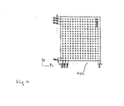
- Fig. 4 emphasizes predetermined measuring points for detecting T( ⁇ ) and R( ⁇ ) on a glass pane (401), whose dimensions are e.g. 1100 x 1300 mm.
- the measuring points simultaneously determine a measuring pattern, comprising e.g. 441 data points, which are e.g. offset by 63 mm in the direction of the Y-axis illustrated in Fig. 4 , and offset by 53 mm in the direction of the X-axis.
- the exterior measurement points are offset e.g. by 20 mm from the edge of the glass pane.
- the measuring time can e.g. be 15 min.
- the measurement or control computer 203 illustrated in Fig. 2 can initially determine e.g. the measurement points illustrated in Fig. 4 for the large area measurement system, which is being used. Furthermore, additional measurement parameters can be defined for transmission and reflection measurements, like e.g. a particular scan speed or a particular scan precision.
- the analysis- or processing computer 207 which is used for OGB determination, there while is e.g. in a standby condition.
- a relevant spectral range can furthermore be predetermined at the processing computer 207, wherein the processing can e.g. be performed using the previously mentioned fit-software.
- the result thus obtained is subjected to an evaluation, in order to determine, if the theoretically calculated spectral distribution or spectral value differs from the measurement result, and what size the difference may be.
- differences which are e.g. smaller than 0.5%, can become negligible. It may be possible to improve the measurement concept by effectuating a change, which causes a smaller difference between the theoretically computed spectral value and the measurement result. Furthermore, the spectral value can be changed.
- an additional measurement T( ⁇ ) and R( ⁇ ) can be manually performed, e.g. by means of the measurement computer 203, in another area of interest, wherein processing of the measurement results is performed at the analysis computer 207 for the additional location(s), using the fit-software, wherein each result is described as mentioned above.
- an automatic measurement can be initiated e.g. by means of a measurement computer 203, wherein the previously programmed measurement points are sequentially approached, and wherein T( ⁇ ) and R( ⁇ ) are measured at predetermined locations.
- the analysis computer 207 can begin automatic processing, thus it is being initially monitored, if e.g. an expected spectral pair T( ⁇ ) is present for a measurement point, e.g. for a first measurement point. If the result of the test is positive, T( ⁇ ) and R( ⁇ ) can be loaded, wherein the processing is performed according to a measurement concept. Thus, e.g. the layer thickness and/or the energy band gap Eg can be determined for said point.
- ⁇ ⁇ , A, C, and E 0 can be computed. Subsequently, it can be monitored, if a next expected spectral pair T( ⁇ ) and R( ⁇ ) is present, wherein the above described method is continued until the last predetermined measurement point has been considered.
- the results of the processing can e.g. be stored in the analysis computer 207. Finally, the measurement computer 203 and the analysis computer 207 can be put into a standby mode until another sample is being measured.
- the method according to the invention can e.g. be used to determine the optical band gap at solar absorption layers, deposited on a large area.
- the exemplary large area measurement system illustrated in Fig. 2 can e.g. be used for determining the spectral transmission T( ⁇ ) and the reflection R( ⁇ ), which measures said values in predetermined portions of the optical layer.
Landscapes
- Physics & Mathematics (AREA)
- General Physics & Mathematics (AREA)
- Analytical Chemistry (AREA)
- Health & Medical Sciences (AREA)
- Life Sciences & Earth Sciences (AREA)
- Chemical & Material Sciences (AREA)
- Biochemistry (AREA)
- General Health & Medical Sciences (AREA)
- Immunology (AREA)
- Pathology (AREA)
- Mathematical Physics (AREA)
- Length Measuring Devices By Optical Means (AREA)
- Investigating Or Analysing Materials By Optical Means (AREA)
Priority Applications (3)
| Application Number | Priority Date | Filing Date | Title |
|---|---|---|---|
| EP08009845A EP2128603A1 (fr) | 2008-05-29 | 2008-05-29 | Procédé pour déterminer une propriété optique d'une couche optique |
| PCT/EP2009/001800 WO2009143921A1 (fr) | 2008-05-29 | 2009-03-12 | Procédé permettant de déterminer une propriété optique d'une couche optique |
| TW98109258A TW200949230A (en) | 2008-05-29 | 2009-03-20 | A method for determining an optical property of an optical layer |
Applications Claiming Priority (1)
| Application Number | Priority Date | Filing Date | Title |
|---|---|---|---|
| EP08009845A EP2128603A1 (fr) | 2008-05-29 | 2008-05-29 | Procédé pour déterminer une propriété optique d'une couche optique |
Publications (1)
| Publication Number | Publication Date |
|---|---|
| EP2128603A1 true EP2128603A1 (fr) | 2009-12-02 |
Family
ID=39758805
Family Applications (1)
| Application Number | Title | Priority Date | Filing Date |
|---|---|---|---|
| EP08009845A Withdrawn EP2128603A1 (fr) | 2008-05-29 | 2008-05-29 | Procédé pour déterminer une propriété optique d'une couche optique |
Country Status (1)
| Country | Link |
|---|---|
| EP (1) | EP2128603A1 (fr) |
Cited By (1)
| Publication number | Priority date | Publication date | Assignee | Title |
|---|---|---|---|---|
| KR20180011146A (ko) * | 2015-05-21 | 2018-01-31 | 케이엘에이-텐코 코포레이션 | 광 분산의 다중 발진기, 연속 코디 로렌츠 모델 |
Citations (2)
| Publication number | Priority date | Publication date | Assignee | Title |
|---|---|---|---|---|
| US20020191192A1 (en) * | 2001-05-15 | 2002-12-19 | Matthias Patzwald | Method and arrangement for contactless determination of product characteristics |
| US20060007430A1 (en) | 2004-07-09 | 2006-01-12 | Hans-Georg Lotz | Method of determining physical properties of an optical layer or layer system |
-
2008
- 2008-05-29 EP EP08009845A patent/EP2128603A1/fr not_active Withdrawn
Patent Citations (3)
| Publication number | Priority date | Publication date | Assignee | Title |
|---|---|---|---|---|
| US20020191192A1 (en) * | 2001-05-15 | 2002-12-19 | Matthias Patzwald | Method and arrangement for contactless determination of product characteristics |
| US20060007430A1 (en) | 2004-07-09 | 2006-01-12 | Hans-Georg Lotz | Method of determining physical properties of an optical layer or layer system |
| EP1632746A1 (fr) | 2004-09-07 | 2006-03-08 | Applied Films GmbH & Co. KG | Procédé pour déterminer des paramètres physiques d'une couche optique ou d'un ensemble de couches |
Non-Patent Citations (5)
| Title |
|---|
| APPLIED PHYSICS LETTERS, 13 September 1996 (1996-09-13) |
| F. JELLISON; MODENE: "Parameterization of the optical functions of amorphous materials in the inter band region", APPLIED PHYSICS LETTERS, vol. 69, no. 3, 15 July 1996 (1996-07-15) |
| FERLAUTO A S ET AL: "Analytical model for the optical functions of amorphous semiconductors and its applications for thin film solar cells", THIN SOLID FILMS, ELSEVIER-SEQUOIA S.A. LAUSANNE, CH, vol. 455-456, 1 May 2004 (2004-05-01), pages 388 - 392, XP004504814, ISSN: 0040-6090 * |
| FERLAUTO A S ET AL: "Analytical model for the optical functions of amorphous semiconductors from the near-infrared to ultraviolet: Applications in thin film photovoltaics", JOURNAL OF APPLIED PHYSICS, AMERICAN INSTITUTE OF PHYSICS. NEW YORK, US, vol. 92, no. 5, 1 September 2002 (2002-09-01), pages 2424 - 2436, XP012057136, ISSN: 0021-8979 * |
| MROZ B ET AL: "Influence of hydrogen on optical properties of LPCVD amorphous silicon films", CONFERENCE RECORD OF THE 26TH IEEE PHOTOVOLTAIC SPECIALISTS CONFERENCE 19970929; 19970929 - 19971003 NEW YORK, NY : IEEE, US, 29 September 1997 (1997-09-29), pages 671 - 673, XP010267874, ISBN: 978-0-7803-3767-1 * |
Cited By (1)
| Publication number | Priority date | Publication date | Assignee | Title |
|---|---|---|---|---|
| KR20180011146A (ko) * | 2015-05-21 | 2018-01-31 | 케이엘에이-텐코 코포레이션 | 광 분산의 다중 발진기, 연속 코디 로렌츠 모델 |
Similar Documents
| Publication | Publication Date | Title |
|---|---|---|
| EP0696345B1 (fr) | Ellipsometre a alignement automatique in situ et procede d'utilisation pour le controle de traitement | |
| US7478019B2 (en) | Multiple tool and structure analysis | |
| US7099005B1 (en) | System for scatterometric measurements and applications | |
| US7522294B2 (en) | Measuring a process parameter of a semiconductor fabrication process using optical metrology | |
| EP2726849B1 (fr) | Mesure de cote critique | |
| KR102504761B1 (ko) | 박막 특성 측정 방법 | |
| US20060117293A1 (en) | Method for designing an overlay mark | |
| WO2009143921A1 (fr) | Procédé permettant de déterminer une propriété optique d'une couche optique | |
| GB2380258A (en) | Measurement of thickness and optical characteristics of multi-layer films | |
| US20160291633A1 (en) | Integrated computational element fabrication methods and systems | |
| Bergese et al. | A simple solution to systematic errors in density determination by X-ray reflectivity: The XRR-density evaluation (XRR-DE) method | |
| EP2251638B1 (fr) | Procédé et appareil pour déterminer l'épaisseur de couche et l'indice de réfraction d'un échantillon | |
| US20090296100A1 (en) | Method for determining an optical property of an optical layer | |
| EP1221583A1 (fr) | Méthode de mesure de l'épaisseur d'une couche ultra-mince d'oxyde | |
| US11680791B2 (en) | Methods and systems for real-time, in-process measurement of coatings on substrates of aerospace components | |
| US20050006585A1 (en) | System and method for correction for angular spread in determining optical properties of materials | |
| US7202958B1 (en) | Modeling a sample with an underlying complicated structure | |
| CN115096823B (zh) | 薄膜结构检测方法、装置、电子设备及存储介质 | |
| CN114324184B (zh) | 椭偏仪光谱浮动模型及建立方法 | |
| CN110793987B (zh) | 一种测试方法及装置 | |
| Theiss | Analysis of optical spectra by computer simulation-from basics to batch mode | |
| US20070171429A1 (en) | Method for calculating a model spectrum | |
| Odarych et al. | Determination of parameters of cadmium telluride films on silicon by the methods of main angle and multiangular ellipsometry. |
Legal Events
| Date | Code | Title | Description |
|---|---|---|---|
| PUAI | Public reference made under article 153(3) epc to a published international application that has entered the european phase |
Free format text: ORIGINAL CODE: 0009012 |
|
| 17P | Request for examination filed |
Effective date: 20080529 |
|
| AK | Designated contracting states |
Kind code of ref document: A1 Designated state(s): AT BE BG CH CY CZ DE DK EE ES FI FR GB GR HR HU IE IS IT LI LT LU LV MC MT NL NO PL PT RO SE SI SK TR |
|
| AX | Request for extension of the european patent |
Extension state: AL BA MK RS |
|
| AKX | Designation fees paid |
Designated state(s): AT BE BG CH CY CZ DE DK EE ES FI FR GB GR HR HU IE IS IT LI LT LU LV MC MT NL NO PL PT RO SE SI SK TR |
|
| STAA | Information on the status of an ep patent application or granted ep patent |
Free format text: STATUS: THE APPLICATION IS DEEMED TO BE WITHDRAWN |
|
| 18D | Application deemed to be withdrawn |
Effective date: 20121201 |