EP2129013A1 - Circuit de contrôle pour surveiller les propriétés de ligne de transmission de fibre optique et la qualité du signal optique - Google Patents
Circuit de contrôle pour surveiller les propriétés de ligne de transmission de fibre optique et la qualité du signal optique Download PDFInfo
- Publication number
- EP2129013A1 EP2129013A1 EP09170524A EP09170524A EP2129013A1 EP 2129013 A1 EP2129013 A1 EP 2129013A1 EP 09170524 A EP09170524 A EP 09170524A EP 09170524 A EP09170524 A EP 09170524A EP 2129013 A1 EP2129013 A1 EP 2129013A1
- Authority
- EP
- European Patent Office
- Prior art keywords
- optical
- optical signal
- signal
- unit
- electric field
- Prior art date
- Legal status (The legal status is an assumption and is not a legal conclusion. Google has not performed a legal analysis and makes no representation as to the accuracy of the status listed.)
- Withdrawn
Links
Images







Classifications
-
- H—ELECTRICITY
- H04—ELECTRIC COMMUNICATION TECHNIQUE
- H04B—TRANSMISSION
- H04B10/00—Transmission systems employing electromagnetic waves other than radio-waves, e.g. infrared, visible or ultraviolet light, or employing corpuscular radiation, e.g. quantum communication
- H04B10/60—Receivers
- H04B10/66—Non-coherent receivers, e.g. using direct detection
- H04B10/69—Electrical arrangements in the receiver
- H04B10/697—Arrangements for reducing noise and distortion
- H04B10/6971—Arrangements for reducing noise and distortion using equalisation
-
- H—ELECTRICITY
- H04—ELECTRIC COMMUNICATION TECHNIQUE
- H04B—TRANSMISSION
- H04B10/00—Transmission systems employing electromagnetic waves other than radio-waves, e.g. infrared, visible or ultraviolet light, or employing corpuscular radiation, e.g. quantum communication
- H04B10/07—Arrangements for monitoring or testing transmission systems; Arrangements for fault measurement of transmission systems
- H04B10/075—Arrangements for monitoring or testing transmission systems; Arrangements for fault measurement of transmission systems using an in-service signal
- H04B10/079—Arrangements for monitoring or testing transmission systems; Arrangements for fault measurement of transmission systems using an in-service signal using measurements of the data signal
- H04B10/0795—Performance monitoring; Measurement of transmission parameters
Definitions
- the present invention relates to a monitor method and a monitor circuit for monitoring a property of an optical fiber transmission line and the quality of an optical signal transmitted via the optical fiber transmission line, and to an optical receiver including the monitor circuit.
- An optical communications system using an optical fiber transmission line generally offers a high-speed data transmission, by which an enormous amount of information is transmitted/received. Therefore, heavy damage may possibly occur if the data transmission is halted. Accordingly, methods for monitoring the property of an optical transmission line or the quality of an optical signal are proposed. Monitoring an optical transmission line and an optical signal is effective also at efficiently operating an optical communications system.
- Patent Document 1 Japanese Patent Publication No. 2001-194267 recites the method for evaluating the quality of an optical signal.
- the method recited in Patent Document 1 includes the following steps: converting an optical signal into an intensity-modulated electric signal; measuring the intensity distribution of the optical signal by sampling the intensity-modulated electric signal; obtaining an amplitude histogram from the intensity distribution of the optical signal; obtaining two local maximum values from the amplitude histogram, and estimating a distribution function g1 equivalent to "level 1" and a distribution function g0 equivalent to "level 0" by using the two local maximum values; obtaining the average intensity values and the standard deviation values of the "level 1" and "level 2" from the distribution functions g1 and g0; and evaluating a signal-to-noise ratio on the basis of the average intensity values and the standard deviation values.
- the quality of an optical signal is monitored by using the intensity information.
- a plurality of monitor devices must be implemented to monitor a plurality of types of properties, leading to an obstacle to the downsizing and/or the cost-cutting of an optical receiver.
- An object of the embodiments is to downsize and/or cost-cut a monitor circuit for monitoring a property of an optical fiber transmission line and the quality of an optical signal.
- An optical receiver comprises an optical reception circuit adapted to perform coherent reception of an optical signal transmitted via an optical fiber transmission line; a digital equalization filter adapted to perform a filter computation to compensate for dispersion of the optical fiber transmission line, according to complex electric field data of the optical signal, which is obtained with the coherent reception; and a property detecting unit adapted to detect a property of the optical fiber transmission line by using parameters set in the digital equalization filter to compensate for the dispersion.
- a disclosed monitor circuit is used along with an optical reception circuit for performing coherent reception of an optical signal, and includes a digital equalization filter for generating equalized electric field data by filter computation to equalize the optical signal, for electric field data of the optical signal, which is obtained with coherent reception, and a quality calculating unit for calculating the quality of the optical signal on the basis of the equalized electric field data.
- another disclosed monitor circuit is used along with an optical reception circuit for performing coherent reception of an optical signal transmitted via an optical fiber transmission line, and includes a digital equalization filter for performing a filter computation to compensate for a property of the optical fiber transmission line, for electric field data of the optical signal, which is obtained with the coherent reception, and a property detecting unit for detecting the property of the optical fiber transmission line by using at least one parameter for determining a transfer function of the digital equalization filter to compensate for the property.
- Fig. 1A and 1B are schematic diagrams illustrating a configuration of an optical communications system using a monitor device according to an embodiment.
- the optical communications system illustrated in Fig. 1 is configured by including an optical transmitter 1, an optical receiver 2, and an optical fiber transmission line 3 connecting the optical transmitter 1 and the optical receiver 2.
- One or a plurality of optical repeater stations (optical amplifiers) 4 may be provided on the transmission line 3.
- An optical signal transmitted from the optical transmitter 1 is, for example, an optical PSK (Phase Shift Keying) signal, an optical QAM (Quadrature Amplitude Modulation) signal, or an optical FM (Frequency Modulation) signal although it is not particularly limited.
- PSK Phase Shift Keying
- QAM Quadrature Amplitude Modulation
- FM Frequency Modulation
- PSK includes DPSK (Differential PSK).
- the optical receiver 2 includes a monitor circuit 5.
- the monitor circuit 5 monitors not only the state of the optical fiber transmission line 3 but also the quality of an optical signal transmitted via the optical fiber transmission line 3.
- the monitor circuit 5 may be provided only in the optical receiver 2 as illustrated in Fig. 1A , or provided in an arbitrary or all of optical repeater stations 4 as illustrated in Fig. 1B .
- Results of the monitoring made by the monitor circuit 5 may be notified, for example, to a network management system (NMS) 6.
- NMS network management system
- the network management system 6 issues an alarm when the state of the optical fiber transmission line 3 or the quality of an optical signal deteriorates, and issues an instruction to change the system configuration if necessary. For example, if the optical fiber transmission line 3 is redundantly configured, the network management system 6 may switch between an active system and a standby system according to a notification made from the monitor circuit 5.
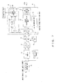
- Fig. 2 is a block diagram illustrating a configuration of an optical receiver including a monitor circuit according to a first embodiment.
- This optical receiver is configured by including an optical reception circuit 10 for making coherent reception of an optical signal, and a digital signal processing unit (DSP) 20 provided at a stage succeeding the optical reception circuit 10.
- DSP digital signal processing unit
- the monitor circuit is implemented with the digital signal processing unit 20 and this will be described in detail later.
- an input optical signal is an optical mPSK signal.
- the optical reception circuit 10 includes a local light source 11, a polarization control unit 12, an optical hybrid unit 13, photo reception units 14, a clock recovery unit 15, and A/D converters 16.
- the local light source 11 generates a local light with almost the same frequency as that of an input light.
- the local light is, for example, continuous wave light.
- the polarization control unit 12 controls the polarization of the input light so that the polarizations of the input light and the local light match.
- the optical hybrid unit 13 combines the input light and the local light, and also combines the input light and the local light with a different optical phase by 90 degree from above one. As a result, an I-component optical signal and a Q-component optical signal are obtained.
- the photo reception units 14 are respectively configured, for example, by including a photodiode, and respectively convert the I-component optical signal and the Q-component optical signal into electric signals.
- the clock recovery unit 15 recovers from an input signal a clock synchronous with the symbol rate of a signal transmitted by the signal light.
- the A/D converters 16 convert one pair of electric signals obtained from the photo reception units 14 into digital data by using the recovered clock.
- I-component data and Q-component data are obtained.
- one pair of I-component data and Q-component data represents one complex number.
- the I-component data represents the value of a real part of a complex number
- the Q-component data represents the value of an imaginary part of the complex number.
- the I-component data and the Q-component data represent the optical electric field (optical amplitude and optical phase) of an input optical signal.
- the optical reception circuit 10 generates optical electric field data of an input signal light with coherent reception.
- “coherent reception” is not limited to the method using a local light as illustrated in Fig. 2 , and assumed to include also self-coherent reception that does not use a local light. Namely, "coherent reception” is assumed to indicate a reception method by which optical amplitude information and optical phase information is obtained.
- the digital signal processing unit 20 includes an FIR filter 21, a phase synchronization unit 22, a signal decision unit 23, a quality monitor unit 24, and a CD monitor unit 25.
- the digital signal processing unit 20 may be realized with a general-purpose processor.
- the dispersion (especially, chromatic dispersion) of the optical fiber transmission line 3 is compensated in the filter computation performed by the FIR filter 21. Namely, the inverse property of the dispersion is provided to the optical electric field data.
- Fig. 3 is a block diagram illustrating an example of the FIR filter 21.
- the FIR filter 21 includes delay elements 31-1 to 31-n, multiplying units 32-0 to 32-n, an adding unit 33, a lock status check unit 34, and a coefficient managing unit 35.
- the delay elements 31-1 to 31-n are connected in series, and respectively delay an input signal by a time ⁇ . Accordingly, signals that are delayed by ⁇ to n x ⁇ are obtained with the delay elements 31-1 to 31-n.
- the multiplying unit 32-0 multiplies the input signal by a coefficient C 0 .
- the multiplying unit 32-1 multiples the output signal of the delay element 31-1 by a coefficient C 1 .
- each of the multiplying units 32-2 to 32-n multiplies the output signal of the corresponding one of the delay elements 31-2 to 31-n by the corresponding one of coefficients C 2 to C n .
- the coefficients C 0 to C n are weighting coefficients to compensate for the waveform distortion (such as an influence exerted by the cumulative chromatic dispersion of the optical fiber transmission line 3) of the input signal.
- the coefficients C 0 to C n are predetermined on the basis of a measurement, a simulation, etc., and managed by the coefficient managing unit 35.
- the adding unit 33 adds up the results of the multiplications made by the multiplying units 32-0 to 32-n.
- the lock status check unit 34 determines, on the basis of the results of the addition obtained by the adding unit 33, whether or not a recovered clock is locked.
- the recovered clock is determined to be locked, for example, if the state of the recovered clock falls within a predetermined range in a predetermined time period.
- the coefficient managing unit 35 holds a plurality of sets of coefficients C 0 to C n .
- the coefficient managing unit 35 outputs the first set of coefficients C 0 to C n at the start of operations, and references the result of the determination obtained by the lock status check unit 34. If the recovered clock is determined not to be locked at this time, the coefficient managing unit 35 changes the coefficients C 0 to C n .
- the coefficient managing unit 35 sequentially changes the coefficients C 0 to C n until the lock status check unit 34 detects the recovered clock is locked. Since the configuration and the operations of the FIR filter are a known technique, their detailed explanations are omitted.
- the phase synchronization unit 22 performs, for the optical electric field data equalized by the FIR filter 21, a computation to compensate for the frequency offset of an optical signal, and a computation to synchronize a phase.
- the frequency offset represents a difference between the frequencies of the input light and the local light.
- a phase error of optical electric field data is initially calculated.
- the phase error is obtained, for example, by raising the optical electric field data to the m-th power. "m” is "m" of mPSK modulation.
- phase-synchronized optical electric field data is obtained by subtracting the phase error from the optical electric field data.
- the signal decision unit 23 decides data for each symbol by comparing one pair of data obtained by the phase synchronization unit 22 with threshold values respectively.
- phase synchronization unit 22 and the signal decision unit 23 are not particularly limited, and may be implemented with a known technique. For example, they are recited in " Satoshi Tsukamoto, Yuta Ishikawa, and Kazuro Kikuchi, 'Optical Homodyne Receiver Comprising Phase and Polarization Diversities with Digital Signal Processing', European Conference On Optical Communication 2006 ".
- the quality monitor unit 24 calculates an Optical Signal-to-Noise Ratio (OSNR) of an optical signal on the basis of the optical electric field data equalized by the FIR filter 21.
- the calculated optical signal-to-noise ratio is notified, for example, to the network management system 6 illustrated in Fig. 1 .
- the CD monitor unit 25 calculates the chromatic dispersion of the optical fiber transmission line 3 by using the tap coefficients of the FIR filter 21 although they are not used in the first embodiment.
- the calculated chromatic dispersion value is notified, for example, to the network management system 6 illustrated in Fig. 1 .
- the optical electric field data is complex digital data that represents the I-component and the Q-component of the optical signal.
- the monitor circuit according to the first embodiment is implemented with the FIR filter 21 and the quality monitor unit 24.
- the FIR filter 21 is used not only to recover data from a received signal but also to monitor the quality of an optical signals.
- Fig. 4 is a flowchart illustrating the procedure for calculating the quality of an optical signal in the first embodiment.
- step S1 an optical signal is equalized by using the FIR filter 21. Namely, the chromatic dispersion of the optical fiber transmission line 3 is compensated.
- Step S1 is executed, for example, each time the A/D converters 16 sample and output optical electric field data. In this case, the optical electric field data of the optical signal is sequentially generated at each sampling timing of the A/D converters 16.
- step S2 the amplitude (namely, the intensity) of the optical signal is calculated from the I-component and the Q-component of the optical electric field data.
- the process of the flowchart illustrated in Fig. 4 is executed over a time period that is sufficiently long with respect to the sampling period of the A/D converters 16, a plurality of amplitude values are obtained.
- the average value and the standard deviation value of the amplitude of the optical signal are calculated by using the plurality of amplitude values.
- the optical signal s equalized by the FIR filter 21 is represented with the following equation.
- Fig. 5 is a schematic diagram illustrating the quality index F OSNR1 .
- the constellation illustrated in Fig. 5 represents the distribution when optical electric field data obtained within a predetermined time period is sampled (downsampling).
- phase synchronization is not performed for data provided to the quality monitor unit 24. Therefore, signal points represented on the constellation are distributed almost evenly in all of phases at almost constant amplitude.
- step S3 an optical signal-to-noise ratio is obtained from the quality index F OSNR1 .
- a relationship between the quality index F OSNR1 and the optical signal-to-noise ratio is obtained in advance with a measurement, a simulation, etc. Assume that the optical signal-to-noise ratio is obtained uniquely from the quality index F OSNR1 as illustrated in Fig. 6 .
- the calculated optical signal-to-noise ratio is output.
- the amplitude of an optical signal is calculated from optical electric field information obtained with coherent reception, and an optical signal-to-noise ratio is calculated from the average value and the standard deviation of the amplitude in the monitor circuit according to the first embodiment.
- Fig. 7 is a block diagram illustrating a configuration of an optical receiver including a monitor circuit according to a second embodiment.
- the basic configuration of the monitor circuit according to the second embodiment is the same as the first embodiment illustrated in Fig. 2 . Note that, however, a configuration and operations of a quality monitor unit 41 included in the monitor circuit according to the second embodiment are different from those of the quality monitor unit 24 in the first embodiment.
- the quality monitor unit 41 includes a filter 42 and a power computing unit 43.
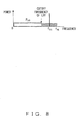
- the filter 42 is an LPF (Low Pass Filter) or a BPF (Band Pass Filter), and implemented, for example, with an FIR filter. If the filter 42 is implemented with an LPF, a cutoff frequency is set to, for example, about "0.6 x f sig ". "f sig " is the symbol rate of data transmitted by the optical signal.
- the BPF is designed to transmit a predetermined bandwidth on the low frequency side of "f sig ".
- Fig. 8 is a schematic diagram illustrating the property of an LPF used as the filter 42.
- f sig is the symbol rate of data transmitted by an optical signal as described above.
- f PD is the frequency band of the photo reception units 14.
- the power computing unit 43 calculates a quality index F OSNR2 by using the optical electric field data output from the FIR filter 21, and the optical electric field data filtered by the filter 42.
- the optical electric field data output from the FIR filter 21 represents the optical electric field of a received optical signal.
- the optical electric field data filtered by the filter 42 represents an ASE component (namely, a noise component).
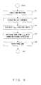
- Fig. 9 is a flowchart illustrating the procedure for calculating the quality of an optical signal in the second embodiment.
- step S11 an optical signal is equalized by using the FIR filter 21 in a similar manner as in step S1 of the first embodiment.
- step S12 an ASE component is extracted with a filter computation by the filter 42.
- a quality index F OSNR2 is calculated from the optical electric field data output from the FIR filter 21, and the optical electric field data filtered by the filter 42.
- the equalized optical signal s namely, the output of the FIR filter 21
- the signal S filtered filtered by the filter 42 is represented with the following equation.
- s k_filtered I k_filtered + jQ k_filtered
- the average power P ave of the optical signal including a data signal is calculated from "s k "
- the power A ASE of the ASE component is calculated from s k_filtered .
- the quality index F OSNR2 is obtained with the following equation (3).
- step S14 an optical signal-to-noise ratio is obtained from the quality index F OSNR2 .
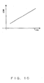
- a relationship between the quality index F OSNR2 and the optical signal-to-noise ratio is obtained in advance with a measurement, a simulation, etc. Assume that the optical signal-to-noise ratio is obtained uniquely from the quality index F OSNR2 as illustrated in Fig. 10 . Note that the relationship between the quality index F OSNR2 and the optical signal-to-noise ratio is usually different from that between the quality index F OSNR1 and the optical signal-to-noise ratio in the first embodiment.
- the calculated optical signal-to-noise ratio is output.
- an ASE component is extracted from optical electric field information obtained with coherent reception, and an optical signal-to-noise ratio is calculated from the power ratio of an optical signal to an ASE component in the monitor circuit according to the second embodiment.
- Fig. 11 is a block diagram illustrating a configuration of an optical receiver including a monitor circuit according to a third embodiment.
- the basic configuration of the monitor circuit according to the third embodiment is the same as the first embodiment illustrated in Fig. 2 . Note that, however, a configuration and operations of a quality monitor unit 51 included in the monitor circuit according to the third embodiment are different from those of the quality monitor unit 24 in the first embodiment.
- the quality monitor unit 51 receives the electric field data of an optical signal after being synchronized, the frequency offset of which is compensated and the phase error of which is removed by the phase synchronization unit 22. Then, the quality monitor unit 51 calculates a quality index F quality on the basis of the optical electric field data after being phase-synchronized.
- Fig. 12 is a flowchart illustrating the procedure for calculating the quality of an optical signal in the third embodiment.
- step S21 an optical signal is equalized by using the FIR filter 21 in a similar manner as in step S1 of the first embodiment.
- step S21 is not an essential procedural step.
- step S22 the frequency offset of the optical signal is compensated for and its phase error is removed by the phase synchronization unit 22. Namely, phase synchronization is established. Accordingly, optical electric field data provided to the quality monitor unit 51 is distributed in the proximities of signal points having an amplitude and a phase, which correspond to a modulation method, as illustrated in Fig. 13. Fig. 13 illustrates the case where an optical QPSK signal is used. In this case, the optical electric field data is distributed in the proximities of four phases ( ⁇ /4, 3 ⁇ /4, 5 ⁇ /4, 7 ⁇ /4).
- step S23 the amplitude (namely, the intensity) of the optical signal is calculated from the I-component and the Q-component of the optical electric field data after being phase-synchronized.
- the process of the flowchart illustrated in Fig. 12 is executed over a predetermined time period that is sufficiently long with respect to the sampling period of the A/D converters 16, a plurality of amplitude values are obtained.
- the average value of the amplitude of the optical signal is calculated by using the plurality of amplitude values.
- the standard deviation value at each signal point is calculated.
- the optical signal s after being phase-synchronized is represented with the following equation.
- step S24 the following quality index F quality is calculated by using the average amplitude ⁇ and the standard deviation value ⁇ , which are obtained with the above provided equations.
- F quality ⁇ / ⁇
- step S24 an evaluation value with high accuracy can be obtained in a short time if the average value of the quality index F quailty , which is obtained at each of signal points (for example, four points in QPSK), is calculated. Moreover, average power used in the second embodiment may be used as a replacement for the average amplitude ⁇ . As described above, the quality of an optical signal is calculated by using optical electric field information after being phase-synchronized in the monitor circuit according to the third embodiment.
- Fig. 14 is a block diagram illustrating a configuration of an optical receiver including a monitor circuit according to a fourth embodiment.
- the basic configuration of the monitor circuit according to the fourth embodiment is the same as the first embodiment illustrated in Fig. 2 . Note that, however, a property of an optical fiber transmission line is detected by using the parameters of the FIR filter 21 in the monitor circuit according to the fourth embodiment.
- the optical receiver illustrated in Fig. 14 is a single polarization coherent receiver. An embodiment for detecting chromatic dispersion as one of properties of an optical fiber transmission line is described below.
- Fig. 15 is a diagram illustrating a structure of a tap coefficient parameter table possessed by the FIR filter 21.
- the tap coefficient table stores tap coefficients to compensate for chromatic dispersion for each of a plurality of chromatic dispersion values.
- the tap coefficients C 0 to C n to compensate for chromatic dispersion in a range from -1000 ps/nm to 1000 ps/nm are stored in the example illustrated in Fig. 15 .
- a transfer function H of the optical fiber is represented with the following equation (6).
- H ⁇ exp - j ⁇ 2 ⁇ ⁇ 2 ⁇ L / 2
- a transfer function for compensating for the chromatic dispersion is represented with the following equation (7).
- H - 1 ⁇ exp j ⁇ 2 ⁇ ⁇ 2 ⁇ L / 2
- Ts is the inverse number of the sampling frequency.
- c k 1 2 ⁇ ⁇ ⁇ ⁇ - ⁇ ⁇ ⁇ exp j ⁇ ⁇ T s 2 ⁇ ⁇ 2 ⁇ L / 2 + j ⁇ k ⁇ d ⁇
- the chromatic dispersion of the optical fiber transmission line is "-1000 ps/nm”
- "C0_m10" to "Cn_m10” are obtained by substituting "-1000 ps/nm” for ⁇ 2 ", and providing "0, 1, 2, ..., n” sequentially to "k” in the equation (8).
- the tap coefficients C o to C n may be obtained with such a calculation, or with a measurement, a simulation, etc.
- Fig. 16 is a flowchart illustrating the procedure for calculating a property of the optical fiber transmission line in the fourth embodiment.
- step S31 an initial value that is predetermined as a chromatic dispersion value is set.
- one of the chromatic dispersion values registered in the tap coefficient table illustrated in Fig. 15 is selected.
- step S32 the tap coefficients C 0 to C n , which correspond to the set chromatic dispersion value, are extracted from the tap coefficient table, and provided to the FIR filter 21. Then, the FIR filter 21 performs a filter computation for an input signal by using the provided tap coefficients. When the tap coefficients corresponding to, for example, "-1000 ps/nm" are provided at this time, the FIR filter 21 performs a computation to compensate for "-1000 ps/nm".
- step S33 an optical signal-to-noise ratio is monitored by using the output data of the FIR filter 21. Monitoring of the optical signal-to-noise ratio is made, for example, in accordance with any of the first to third embodiments although it is not particularly limited. Namely, a quality index F OSNR (an arbitrary one or a plurality of F OSNR1 , F OSNR2 , and F quality ) is calculated. In step S34, the calculated quality index F OSNR is stored in a memory.
- F OSNR an arbitrary one or a plurality of F OSNR1 , F OSNR2 , and F quality
- step S35 the processes in steps S32 to S34 are repeatedly executed while sweeping a chromatic dispersion value to be compensated for. Namely, the tap coefficients corresponding to each chromatic dispersion within the range from -1000 ps/nm to 1000 ps/nm are sequentially set in the FIR filter 21, and the quality index F OSNR is obtained in this embodiment.
- step S36 a chromatic dispersion value that makes the quality index F OSNR best is output. Assuming that the quality index F OSNR becomes best when the tap coefficients corresponding to "-900 ps/nm" are provided to the FIR filter 21, the actual chromatic dispersion of the optical fiber transmission line is estimated to be "-900 ps/nm".
- the chromatic dispersion value of the optical fiber transmission line is obtained, for example, with the following procedure. Firstly, for instance, "-1000 ps/nm" is selected as an initial value from the tap coefficient table, and its corresponding tap coefficients "C0_m10" to "Cn_m10" are extracted. These tap coefficients are set in the FIR filter 21 to perform a filter computation. Then, an optical signal-to-noise ratio is calculated and stored as "F(-1000)" in the memory.
- the tap coefficients respectively corresponding to "-800 ps/nm” to "1000 ps/nm” are set in the FIR filter 21, and corresponding optical signal-to-noise ratios are calculated and stored respectively as “F(-800)” to "F(1000)” in the memory. Then, a value that makes the quality of the optical signal best among "F(-1000)” to "F(1000)” is output. This procedure does not require the calculation of an optical signal-to-noise ratio for all of the chromatic dispersion values registered in the tap coefficient table.
- tap coefficients that make the quality of an optical signal best are searched while changing the tap coefficients of the FIR filter for equalizing an optical signal in the monitor circuit according to the fourth embodiment. Then, the chromatic dispersion value corresponding to the searched tap coefficients is obtained as a property of the optical fiber transmission line.
- Fig. 17 is a flowchart illustrating another procedure executed in the fourth embodiment.
- adaptive waveform equalization is performed in step S41. Namely, a state where the waveform of an optical signal is suitably equalized is searched while the coefficient managing unit 35 is switching among the sets of tap coefficients in the FIR filter 21.
- the tap coefficients C 0 to C n at that time are read from the tap coefficient table in step S42.
- step S43 a chromatic dispersion value is calculated from the read tap coefficients C 0 to C n .
- chromatic dispersion ⁇ 2 is calculated from the tap coefficients C 0 to C n by solving the inverse function of the above provided equation (8).
- step S44 the calculated chromatic dispersion value is output. This procedure eliminates the need for sweeping the entire chromatic dispersion range registered in the tap coefficient table, thereby reducing the computation amount.
- Fig. 18 is a block diagram illustrating a configuration of an optical receiver including a monitor circuit according to a fifth embodiment.
- the basic configuration of the monitor circuit according to the fifth embodiment is the same as the third embodiment illustrated in Fig. 11 . Note that, however, a nonlinear quantity is monitored on the basis of the ratio of an amplitude deviation to a phase deviation of an optical signal by using a nonlinear quantity monitor unit 61 in the monitor circuit according to the fifth embodiment.
- Fig. 19 is a schematic diagram illustrating the nonlinear quantity calculated in the fifth embodiment.
- the distribution of optical electric field data after an optical QPSK modulation signal is phase-synchronized is illustrated.
- the nonlinear quantity F NL is defined with the ratio of a standard deviation ⁇ r in amplitude to a standard deviation ⁇ ⁇ in phase.
- the nonlinear quantity F NL is calculated by the nonlinear quantity monitor unit 61 on the basis of the optical electric field data after being phase-synchronized, which is output from the phase synchronization unit 22.
- the optical signals after being phase-synchronized is represented with the following equation.
- the average amplitude and the average phase are represented with the following equations (9) and (10) respectively.
- the standard deviation ⁇ r in amplitude of the optical signal, and the standard deviation ⁇ ⁇ in phase of the optical signal are represented with the following equations (11) and (12) respectively.
- the nonlinear quantity monitor unit 61 calculates the nonlinear quantity F NL with the following equation.
- F N ⁇ L ⁇ ⁇ / ⁇ r
- the nonlinear quantity is calculated from optical electric field information obtained with coherent reception in the monitor circuit according to the fifth embodiment.
- Fig. 20 is a block diagram illustrating a configuration of an optical receiver including a monitor circuit according to a sixth embodiment.
- the basic configuration of the monitor circuit according to the sixth embodiment is the same as the fifth embodiment illustrated in Fig. 18 .
- the monitor circuit according to the sixth embodiment includes a nonlinear compensation unit 62 for compensating for a nonlinear distortion.
- the nonlinear compensation unit 62 is provided between the FIR filter 21 and the phase synchronization unit 22, or provided at a stage succeeding the phase synchronization unit 22.
- the nonlinear compensation unit 62 compensates for nonlinearity by performing a nonlinear compensation algorithm computation for optical electric field data output from the FIR filter 21.
- the nonlinear compensation algorithm is expressed, for example, with a function ⁇ c represented with the following equation (12).
- ⁇ c r c 2 ⁇ r 2 + c 1 ⁇ r + c 0
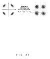
- Fig. 21 is a schematic diagram illustrating the nonlinear compensation made by the nonlinear compensation unit 62.
- a nonlinear effect on an optical phase grows with an increase in an optical amplitude although this is not depicted accurately in Fig. 21 .
- the function ⁇ c rotates the phase of optical electric field data in accordance with the amplitude of the optical electric field data provided to the nonlinear compensation unit 62.
- the nonlinear compensation unit 62 determines the coefficients c 2 to c 0 of the function ⁇ c so that the dispersion of a phase noise is minimized.
- the technique for performing a nonlinear compensation by using the equation (12) is a known technique, and recited in detail, for example, in the following document. " Signal Design and Detection in Presence of Nonlinear Phase Noise", Alan Pak Tao Lau and Joseph Kahn, Journal of Lightwave Technology Vol. 25, No. 10, October 2007 p3008-3016
- a nonlinear quantity monitor unit 63 obtains the coefficients c 2 to c 0 determined by the nonlinear compensation unit 62. Then, the nonlinear quantity monitor unit 63 calculates a nonlinear quantity from the obtained coefficients c 2 to c 0 . Namely, a relationship between the optical amplitude r and the optical phase ⁇ is acquired by providing the obtained coefficients c 2 to c 0 to the equation (12). As a result, the nonlinear quantity is obtained.
- the optical signal transmitted via the optical fiber transmission line is an mPSK signal (especially, a QPSK signal).
- the present invention is not limited to these implementations.
- the monitor circuits according to the embodiments are applicable to not only an mPSK signal but also, for example, a QAM signal, etc.
- the monitor circuits according to the embodiments are also applicable to RZ, NRZ, CSRZ (Carrier Suppressed RZ), and duo binary (PSBT: Phase Shaped Binary Transmission.
- Fig. 22 is a schematic diagram illustrating a method for monitoring the quality of a 16QAM signal.
- the standard deviation ⁇ is calculated for each signal point.
- the standard deviation ⁇ is calculated, for example, with the above provided equation (5).
- the average amplitude ⁇ is calculated for the signal point farthest from the origin point.
- the average amplitude ⁇ is calculated, for example, with the above provided equation (4).
- the optical signal-to-noise ratio of the 16QAM signal is obtained on the basis of " ⁇ / ⁇ ".
- the qualify index may be calculated by using an average power as a replacement for the average amplitude ⁇ .
- the digital signal processing unit 20 may include arbitrary two or more of the monitor circuits according to the first to the sixth embodiments. Namely, the digital signal processing unit 20 may monitor all of an optical signal-to-noise ratio, the chromatic dispersion of an optical fiber transmission line, and a nonlinear quantity. In this case, the monitor computations may be executed in parallel, or executed sequentially in a time-division manner. As described above, the monitor circuits according to the embodiments can calculate various indices (the quality of an optical signal, and properties of an optical fiber transmission line) by using optical electric field information obtained with coherent reception. Accordingly, there is no need to provide devices respectively dedicated to properties to be monitored, thereby downsizing and/or cost-cutting a monitor device for monitoring a plurality of types of properties.
- the above described embodiments refer to a configuration where a monitor circuit is provided within an optical receiver for receiving an optical signal.
- the monitor circuit may be provided in an optical repeater, or the monitor circuit may monitor an optical signal branched at some halfway point of an optical fiber transmission line as described above with reference to Fig. 1 .
- Figs. 23 and 24 are block diagrams illustrating configurations of a monitor circuit that does not have a data recovery function. These monitor circuits are provided, for example, in the optical repeater station 4 illustrated in Fig. 1 .
- the configuration illustrated in Fig. 23 is equivalent, for example, to the first and the second embodiments, and performs monitoring on the basis of a signal the waveform of which is equalized (a signal before being phase-synchronized).
- the phase synchronization unit 22 and the signal decision unit 23, which are illustrated in Fig. 2 , etc. are not required.
- the configuration illustrated in Fig. 24 is equivalent, for example, to the third embodiment, and performs monitoring on the basis of a signal after being phase-synchronized. In this case, the phase synchronization unit 22 is required although the signal decision unit 23 is not required.
- the monitor circuits according to the above described first to sixth embodiments are also applicable to a polarization diversity receiver. Monitoring made in polarization diversity coherent reception is described below.
- Figs. 25 and 26 are block diagrams illustrating configurations of a polarization diversity receiver including the monitor circuit according to any of the embodiments.
- the configuration illustrated in Fig. 25 performs monitoring on the basis of a signal before being phase-synchronized, whereas the configuration illustrated in Fig. 26 performs monitoring on the basis of a signal after being phase-synchronized.
- a polarization beam splitter (PBS) 71 splits input signal light into X-polarization light and Y-polarization light.
- the X-polarization light and the Y-polarization light are guided to optical hybrid units 13x and 13y respectively.
- a polarization beam splitter 72 generates one pair of polarization lights, which are mutually orthogonal, from a local light generated by the local light source 11, and guides the generated lights to optical hybrid units 13x and 13y.
- the optical hybrid unit 13x generates the I-component optical signal and the Q-component optical signal of the X-polarization light of the optical signal.
- the optical hybrid unit 13y generates the I-component optical signal and the Q-component optical signal of the Y-polarization light of the optical signal. Operations of the photo reception units 14, the clock recovery units 15, and the A/D converters 16 are as described above with reference to Fig. 2 .
- the monitor circuit can monitor, for example, Polarization Mode Dispersion (PMD), State Of Polarization (SOP), Polarization Dependent Loss (PDL), etc. in addition to the above described qualities and properties.
- PMD Polarization Mode Dispersion
- SOP State Of Polarization
- PDL Polarization Dependent Loss
- the FIR filter 73 is a butterfly FIR filter including four filter elements as illustrated in Fig. 27 .
- a configuration and operations of each of the filter elements are basically the same as those of the FIR filter described with reference to Fig. 3 .
- the optical electric field data of the X-polarization light is guided to the filter elements FIRxx and FIRxy.
- the optical electric field data of the Y-polarization light is guided to the filter elements FIRyx and FIRyy.
- the filter elements FIRxx and FIRyx make a filter computation to reject the Y-polarization component.
- the filter elements FIRxy and the FIRyy make a filter computation to reject the X-polarization component.
- the filter operations of each of the filter elements are implemented by providing suitable tap coefficients as described above.
- An adder 74 generates optical electric field data X' by adding up the results of the computations made by the filter elements FIRxx and the FIRyx.
- an adder 75 generates optical electric field data Y' by adding up the results of the computations made by the filter elements FIRxy and the FIRyy.
- Operations of the other elements of the digital signal processing unit 20 are basically the same as those in the single polarization coherent reception described with reference to Figs. 2 to 21 . Note that, however, two sets of computations, each set equivalent to the computations performed in the single polarization coherent reception, are executed in the polarization diversity coherent reception.
- the monitor circuit collects tap coefficients that are respectively provided to the filter elements of the FIR filter 73. Namely, the monitor circuit collects four sets of tap coefficients. As a result, the monitor circuit can calculate PMD, SOP, and PDL on the basis of the collected four sets of tap coefficients.
- a method for monitoring SOP by using FIR tap coefficients is described as one example.
- incident polarization light H is represented with the following matrix.
- H ⁇ v 1 v 2 - v 2 * v 1 *
- the inverse matrix of the incident polarization light must be generated to demultiplex a polarization-multiplexed signal.
- the inverse matrix of the incident polarization light is represented as follows.
- H - 1 ⁇ v 1 * - v 2 v 2 * v 1
- This matrix H -1 is implemented by the FIR filter 73. Namely, the computation made by the FIR filter 73 illustrated in Fig. 27 is represented with the following equation.
- a monitor circuit that does not include a data recovery function can be provided even when polarization diversity reception is made.
- a configuration for performing monitoring on the basis of a waveform-equalized signal (namely, a signal before being phase-synchronized) is illustrated in Fig. 28 .
- a configuration for performing monitoring on the basis of a signal after being phase-synchronized is illustrated in Fig. 29 .
- the above described embodiment has referred to the configurations for performing coherent reception by using the local light generated by the local light source 11.
- self-coherent reception that detects the amplitude information and the phase information of an optical signal without using a local light is described below.
- Fig. 30 is a block diagram illustrating a configuration of an optical receiver that performs self-coherent reception.
- input signal light is guided to a delay interferometer circuit 81 and a photo reception unit 84.
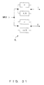
- the delay interferometer circuit 81 is configured, for example, by including two delay interferometers connected in parallel as illustrated in Fig. 31 .
- One of the delay interferometers has a one-sample time delay element in a first arm, and a ⁇ /4 phase shift element in a second arm.
- the other delay interferometer has a one-sample time delay element in a first arm, and a - ⁇ /4 phase shift element in a second arm.
- differential phase information is detected from an input signal light.
- One pair of photo reception units 82 and one pair of A/D converters 83 are provided at stages subsequent to the delay interferometer circuit 81, and digital data that represents a differential phase is obtained.
- the input signal light is converted into an electric signal by the photo reception unit 84, and converted into digital data by an A/D converter 85.
- the amplitude information of the input optical signal is obtained.
- the reconstructed complex electric field data is passed to an MSPE (Multi-Symbol Phase Estimation) unit 87 after being filtered by the FIR filter 21.
- MSPE Multi-Symbol Phase Estimation
- the operations of the quality monitor unit 24 and the CD monitor unit 25 are as described above. Additionally, the quality monitor unit 41, 51, etc. may be used as a replacement for the quality monitor unit 24. Namely, a monitor circuit provided in a coherent receiver using a local light is practically available also in an optical receiver that performs self-coherent reception.
- a self-coherent reception configuration can be introduced into a polarization diversity receiver.
- a configuration where the self-coherent reception is introduced into the polarization diversity receiver is illustrated in Fig. 32 .
- this configuration for example, not only an optical signal-to-noise ratio but also polarization mode dispersion, a state of polarization, and a polarization-dependent loss can be monitored.
- the above described embodiments refer to the cases where an FIR filter is used as one type of a digital equalization filter.
- an IIR filter, a nonlinear filter, etc. may be available as the digital equalization filter.
- the tap coefficients referred to in the above described embodiments are to be understood generally as the operational parameters of a filter, which stipulate the transfer function of the filter.
Landscapes
- Physics & Mathematics (AREA)
- Electromagnetism (AREA)
- Engineering & Computer Science (AREA)
- Computer Networks & Wireless Communication (AREA)
- Signal Processing (AREA)
- Optical Communication System (AREA)
- Testing Of Optical Devices Or Fibers (AREA)
Applications Claiming Priority (2)
| Application Number | Priority Date | Filing Date | Title |
|---|---|---|---|
| JP2008041237A JP2009198364A (ja) | 2008-02-22 | 2008-02-22 | 光ファイバ伝送路の特性および光信号の品質をモニタするモニタ回路 |
| EP08017064A EP2093905A1 (fr) | 2008-02-22 | 2008-09-26 | Circuit de contrôle pour surveiller les propriétés de ligne de transmission de fibre optique et la qualité du signal optique |
Related Parent Applications (1)
| Application Number | Title | Priority Date | Filing Date |
|---|---|---|---|
| EP08017064A Division EP2093905A1 (fr) | 2008-02-22 | 2008-09-26 | Circuit de contrôle pour surveiller les propriétés de ligne de transmission de fibre optique et la qualité du signal optique |
Publications (1)
| Publication Number | Publication Date |
|---|---|
| EP2129013A1 true EP2129013A1 (fr) | 2009-12-02 |
Family
ID=40548800
Family Applications (5)
| Application Number | Title | Priority Date | Filing Date |
|---|---|---|---|
| EP09170522A Withdrawn EP2124359A1 (fr) | 2008-02-22 | 2008-09-26 | Circuit de contrôle pour surveiller les propriétés de ligne de transmission de fibre optique et la qualité du signal optique |
| EP08017064A Withdrawn EP2093905A1 (fr) | 2008-02-22 | 2008-09-26 | Circuit de contrôle pour surveiller les propriétés de ligne de transmission de fibre optique et la qualité du signal optique |
| EP09170520A Withdrawn EP2129011A1 (fr) | 2008-02-22 | 2008-09-26 | Circuit de contrôle pour surveiller les propriétés de ligne de transmission de fibre optique et la qualité du signal optique |
| EP09170521A Withdrawn EP2129012A1 (fr) | 2008-02-22 | 2008-09-26 | Circuit de contrôle pour surveiller les propriétés de ligne de transmission de fibre optique et la qualité du signal optique |
| EP09170524A Withdrawn EP2129013A1 (fr) | 2008-02-22 | 2008-09-26 | Circuit de contrôle pour surveiller les propriétés de ligne de transmission de fibre optique et la qualité du signal optique |
Family Applications Before (4)
| Application Number | Title | Priority Date | Filing Date |
|---|---|---|---|
| EP09170522A Withdrawn EP2124359A1 (fr) | 2008-02-22 | 2008-09-26 | Circuit de contrôle pour surveiller les propriétés de ligne de transmission de fibre optique et la qualité du signal optique |
| EP08017064A Withdrawn EP2093905A1 (fr) | 2008-02-22 | 2008-09-26 | Circuit de contrôle pour surveiller les propriétés de ligne de transmission de fibre optique et la qualité du signal optique |
| EP09170520A Withdrawn EP2129011A1 (fr) | 2008-02-22 | 2008-09-26 | Circuit de contrôle pour surveiller les propriétés de ligne de transmission de fibre optique et la qualité du signal optique |
| EP09170521A Withdrawn EP2129012A1 (fr) | 2008-02-22 | 2008-09-26 | Circuit de contrôle pour surveiller les propriétés de ligne de transmission de fibre optique et la qualité du signal optique |
Country Status (3)
| Country | Link |
|---|---|
| US (1) | US20090214201A1 (fr) |
| EP (5) | EP2124359A1 (fr) |
| JP (1) | JP2009198364A (fr) |
Families Citing this family (61)
| Publication number | Priority date | Publication date | Assignee | Title |
|---|---|---|---|---|
| CN101552640B (zh) * | 2008-04-01 | 2012-04-11 | 富士通株式会社 | 滤波器系数变更装置和方法 |
| US8433192B2 (en) * | 2008-12-08 | 2013-04-30 | Ciena Corporation | Dynamic performance monitoring systems and methods for optical networks |
| US9490894B2 (en) * | 2008-12-08 | 2016-11-08 | Ciena Corporation | Coherent probe and optical service channel systems and methods for optical networks |
| CN102326343B (zh) * | 2009-02-20 | 2014-07-02 | 骁阳网络有限公司 | 用于自适应色散补偿的方法和装置 |
| JP5024481B2 (ja) * | 2009-05-07 | 2012-09-12 | 日本電気株式会社 | コヒーレント受信機 |
| US8463121B2 (en) * | 2009-10-09 | 2013-06-11 | Nec Laboratories America, Inc. | Ultra wide-range frequency offset estimation for digital coherent optical receivers |
| JP5370133B2 (ja) * | 2009-12-22 | 2013-12-18 | 富士通株式会社 | 光受信機および受信方法 |
| WO2011083748A1 (fr) * | 2010-01-08 | 2011-07-14 | 日本電気株式会社 | Appareil de réception de lumière cohérente, système de communication par lumière cohérente utilisant celui-ci et procédé de communication par lumière cohérente |
| JP5446944B2 (ja) | 2010-01-29 | 2014-03-19 | 富士通株式会社 | 光ネットワークおよびその制御方法 |
| CN102215189B (zh) * | 2010-04-02 | 2014-12-17 | 富士通株式会社 | 滤波器、相干接收机装置和相干接收方法 |
| JP5549333B2 (ja) | 2010-04-07 | 2014-07-16 | 富士通株式会社 | 偏波変動補償装置および光通信システム |
| US8494368B2 (en) * | 2010-04-16 | 2013-07-23 | Alcatel Lucent | Electronic nonlinearity compensation for optical transmission systems |
| JP5631636B2 (ja) * | 2010-06-07 | 2014-11-26 | アンリツ株式会社 | Osnr評価装置及びosnr評価方法 |
| JP5462086B2 (ja) * | 2010-06-23 | 2014-04-02 | アンリツ株式会社 | 光コヒーレント検波器評価装置及び光コヒーレント検波器評価方法 |
| JP5598172B2 (ja) * | 2010-08-30 | 2014-10-01 | 富士通株式会社 | 光受信器、光受信方法、および光伝送システム |
| US8705986B2 (en) * | 2010-11-23 | 2014-04-22 | Infinera Corporation | PMD-insensitive method of chromatic dispersion estimation for a coherent receiver |
| JP5633352B2 (ja) * | 2010-12-09 | 2014-12-03 | 富士通株式会社 | デジタルコヒーレント光受信器、適応等化型イコライザ及びデジタルコヒーレント光通信方法 |
| US20120170929A1 (en) * | 2011-01-03 | 2012-07-05 | Chongjin Xie | Apparatus And Method For Monitoring An Optical Coherent Network |
| JP5120507B2 (ja) * | 2011-02-01 | 2013-01-16 | 日本電気株式会社 | 光受信器、偏光分離装置および偏光分離方法 |
| JP5692245B2 (ja) * | 2011-02-02 | 2015-04-01 | 日本電気株式会社 | 光受信機および光受信方法 |
| JP5736837B2 (ja) * | 2011-02-23 | 2015-06-17 | 富士通株式会社 | 光受信装置 |
| JP5099241B2 (ja) * | 2011-03-15 | 2012-12-19 | オムロン株式会社 | 無線通信監視装置、無線通信監視システム、無線通信監視方法、プログラムおよび記録媒体 |
| JP5583631B2 (ja) * | 2011-05-10 | 2014-09-03 | 日本電信電話株式会社 | デジタルコヒーレント受信装置 |
| CN104145432B (zh) * | 2012-03-02 | 2016-08-24 | 日本电气株式会社 | 接收器、传输系统、用于接收偏振复用光学信号的方法,以及存储接收器控制程序的非瞬态计算机可读介质 |
| JP2013192191A (ja) * | 2012-03-15 | 2013-09-26 | Mitsubishi Electric Corp | 光ネットワーク制御方法、光ネットワーク |
| JP5888056B2 (ja) | 2012-03-28 | 2016-03-16 | 富士通株式会社 | デジタル光コヒーレント伝送装置 |
| JP6019887B2 (ja) | 2012-07-26 | 2016-11-02 | 富士通株式会社 | 光伝送システムおよび光伝送路の偏波依存特性をモニタする方法 |
| JP6015291B2 (ja) * | 2012-09-24 | 2016-10-26 | 沖電気工業株式会社 | 光信号品質評価装置及び光信号品質評価方法 |
| JP5978925B2 (ja) * | 2012-11-01 | 2016-08-24 | 富士通株式会社 | 光デジタルコヒーレント受信器 |
| US20140193165A1 (en) * | 2013-01-08 | 2014-07-10 | Silicon Image, Inc. | Electronic alignment of optical signals |
| US9853765B2 (en) | 2013-04-09 | 2017-12-26 | Nec Corporation | Signal processing device and signal processing method for optical polarization multiplexed signal |
| JP6093235B2 (ja) * | 2013-05-01 | 2017-03-08 | Kddi株式会社 | 光通信の品質情報の監視装置 |
| US9479252B2 (en) * | 2013-05-09 | 2016-10-25 | Zte Corporation | Pre-equalization using phase correction |
| CN104348544B (zh) * | 2013-08-05 | 2017-11-10 | 北京凌云光子技术有限公司 | 测量光传输信道质量参数的方法及装置 |
| JP6093273B2 (ja) * | 2013-08-30 | 2017-03-08 | 日本電信電話株式会社 | ペナルティ算出方法、ペナルティ算出器、及びデジタルコヒーレント光伝送システム |
| JP6020521B2 (ja) * | 2014-07-16 | 2016-11-02 | 横河電機株式会社 | 光ファイバ温度分布測定装置 |
| JP6519117B2 (ja) | 2014-08-04 | 2019-05-29 | 富士通株式会社 | 光伝送装置、光伝送システム、及び、光伝送システムの制御装置 |
| EP3021542B1 (fr) * | 2014-11-14 | 2018-09-26 | ZTE Corporation | Post-égalisation itérative pour des récepteurs optiques cohérents |
| JP6380136B2 (ja) * | 2015-01-30 | 2018-08-29 | 富士通株式会社 | 推定装置、及び、推定方法 |
| CN106559133B (zh) * | 2015-09-28 | 2020-02-14 | 华为技术有限公司 | 光信号检测的方法及其网络设备 |
| WO2017077703A1 (fr) * | 2015-11-04 | 2017-05-11 | 日本電気株式会社 | Dispositif et procédé de traitement de signal reçu |
| JP6657885B2 (ja) * | 2015-12-07 | 2020-03-04 | 富士通株式会社 | データ収集装置及び光伝送システム |
| JP6759742B2 (ja) * | 2016-06-16 | 2020-09-23 | 富士通株式会社 | 受信装置及び設定方法 |
| US9979472B1 (en) * | 2016-12-29 | 2018-05-22 | Juniper Networks, Inc. | Methods and apparatus for detecting and compensating power imbalance and modulation imperfection for a coherent optical transmitter |
| JP6885093B2 (ja) | 2017-02-16 | 2021-06-09 | 富士通株式会社 | 伝送路監視装置及び伝送路の監視方法 |
| JP6640139B2 (ja) * | 2017-03-16 | 2020-02-05 | Kddi株式会社 | 障害判定装置及びその制御方法、プログラム、並びに光ファイバ通信システム |
| JP6870423B2 (ja) | 2017-03-29 | 2021-05-12 | 富士通株式会社 | 信号品質測定装置及び信号品質測定方法 |
| JP6659613B2 (ja) * | 2017-03-31 | 2020-03-04 | 日本電信電話株式会社 | 偏波状態推定方法及び偏波状態推定装置 |
| JP6824861B2 (ja) * | 2017-10-25 | 2021-02-03 | 日本電信電話株式会社 | Otdr装置 |
| US10236982B1 (en) * | 2017-12-21 | 2019-03-19 | Ciena Corporation | Fiber parameter identification |
| US11342990B2 (en) * | 2018-02-13 | 2022-05-24 | Nippon Telegraph And Telephone Corporation | State estimating device and communication system |
| RU193600U1 (ru) * | 2019-02-13 | 2019-11-06 | Открытое акционерное общество "СУПЕРТЕЛ" | Устройство для автоматизированного тестирования многоканальных оптических функциональных модулей оборудования цифровых волоконно-оптических систем передачи информации |
| WO2021038677A1 (fr) * | 2019-08-26 | 2021-03-04 | 三菱電機株式会社 | Récepteur |
| JP7315928B2 (ja) * | 2020-07-02 | 2023-07-27 | 日本電信電話株式会社 | 光信号サンプリング装置及び光信号サンプリング方法 |
| US12395244B2 (en) * | 2020-12-02 | 2025-08-19 | Nec Laboratories America, Inc. | Optical fiber exhibiting low guided acoustic Brillouin scattering (GAWBS) noise and measurement thereof |
| US11405104B1 (en) * | 2021-09-16 | 2022-08-02 | Huawei Technologies Co., Ltd. | Method and system for longitudinal performance monitoring of an optical communication line |
| CN113556173B (zh) * | 2021-09-18 | 2021-12-07 | 北京邮电大学 | 非线性区光信噪比监测方法和装置 |
| WO2023119673A1 (fr) | 2021-12-24 | 2023-06-29 | 学校法人明治大学 | Dispositif d'évaluation, récepteur de lumière, système de communication optique, programme, et procédé d'évaluation |
| CN115225162B (zh) * | 2022-08-29 | 2023-01-24 | 北京中科国光量子科技有限公司 | 一种基于往返式延迟干涉仪的集成自相干接收光芯片 |
| CN116388882B (zh) * | 2023-03-31 | 2025-07-15 | 华南理工大学 | 一种光通信系统非线性补偿方法、装置及存储介质 |
| CN119522545B (zh) | 2023-06-22 | 2026-01-13 | 学校法人明治大学 | 控制装置、补偿装置、程序以及控制方法 |
Citations (4)
| Publication number | Priority date | Publication date | Assignee | Title |
|---|---|---|---|---|
| JP2001194267A (ja) | 2000-01-06 | 2001-07-19 | Nippon Telegr & Teleph Corp <Ntt> | 光信号品質評価方法および光信号品質評価装置並びに記憶媒体 |
| US20050019042A1 (en) * | 2003-07-25 | 2005-01-27 | Noriaki Kaneda | Method and apparatus for electronic equalization in optical communication systems |
| US20060013597A1 (en) * | 2004-07-14 | 2006-01-19 | Crivelli Diego E | Compensating impairments of optical channel using adaptive equalization |
| US20080031633A1 (en) * | 2006-07-31 | 2008-02-07 | Fujitsu Limited | Multi-level modulation receiving device |
Family Cites Families (14)
| Publication number | Priority date | Publication date | Assignee | Title |
|---|---|---|---|---|
| FR2726417A1 (fr) * | 1994-10-26 | 1996-05-03 | Philips Electronique Lab | Systeme de transmission et recepteur de signaux a repartition multiplexee de frequences orthogonales muni d'un dispositif de synchronisation de frequences |
| US6304594B1 (en) * | 1998-07-27 | 2001-10-16 | General Dynamics Government Systems Corporation | Interference detection and avoidance technique |
| JP3547622B2 (ja) * | 1998-08-31 | 2004-07-28 | 三菱電機株式会社 | 光信号品質監視装置 |
| US7076169B2 (en) * | 2000-09-26 | 2006-07-11 | Celight, Inc. | System and method for orthogonal frequency division multiplexed optical communication |
| US7054375B2 (en) * | 2000-12-22 | 2006-05-30 | Nokia Corporation | Method and apparatus for error reduction in an orthogonal modulation system |
| US7079765B2 (en) * | 2001-03-07 | 2006-07-18 | Nippon Telegraph And Telephone Corporation | Optical wavelength division multiplex signal monitoring apparatus |
| JP2003218967A (ja) * | 2002-01-17 | 2003-07-31 | Fujitsu General Ltd | タイミング同期方法 |
| US6915084B2 (en) * | 2002-09-03 | 2005-07-05 | Stratalight Communications, Inc. | Optical compensator having compensation for Kerr effect phase noise |
| WO2004095740A1 (fr) * | 2003-04-23 | 2004-11-04 | Mitsubishi Denki Kabushiki Kaisha | Recepteur optique et systeme d'emission optique |
| US7266310B1 (en) * | 2003-04-29 | 2007-09-04 | Nortel Networks Limited | Digital compensation for optical transmission system |
| US7254325B2 (en) * | 2003-05-06 | 2007-08-07 | Fujitsu Limited | Method and system for optical performance monitoring |
| JP3936937B2 (ja) * | 2003-08-27 | 2007-06-27 | 株式会社日立国際電気 | デジタル無線通信システムにおけるポーリング方法および車両検索方法 |
| US7555227B2 (en) * | 2005-10-21 | 2009-06-30 | Nortel Networks Limited | Polarization compensation in a coherent optical receiver |
| JP2009094777A (ja) * | 2007-10-09 | 2009-04-30 | Nec Corp | 信号波形劣化補償回路 |
-
2008
- 2008-02-22 JP JP2008041237A patent/JP2009198364A/ja active Pending
- 2008-09-23 US US12/236,028 patent/US20090214201A1/en not_active Abandoned
- 2008-09-26 EP EP09170522A patent/EP2124359A1/fr not_active Withdrawn
- 2008-09-26 EP EP08017064A patent/EP2093905A1/fr not_active Withdrawn
- 2008-09-26 EP EP09170520A patent/EP2129011A1/fr not_active Withdrawn
- 2008-09-26 EP EP09170521A patent/EP2129012A1/fr not_active Withdrawn
- 2008-09-26 EP EP09170524A patent/EP2129013A1/fr not_active Withdrawn
Patent Citations (4)
| Publication number | Priority date | Publication date | Assignee | Title |
|---|---|---|---|---|
| JP2001194267A (ja) | 2000-01-06 | 2001-07-19 | Nippon Telegr & Teleph Corp <Ntt> | 光信号品質評価方法および光信号品質評価装置並びに記憶媒体 |
| US20050019042A1 (en) * | 2003-07-25 | 2005-01-27 | Noriaki Kaneda | Method and apparatus for electronic equalization in optical communication systems |
| US20060013597A1 (en) * | 2004-07-14 | 2006-01-19 | Crivelli Diego E | Compensating impairments of optical channel using adaptive equalization |
| US20080031633A1 (en) * | 2006-07-31 | 2008-02-07 | Fujitsu Limited | Multi-level modulation receiving device |
Non-Patent Citations (2)
| Title |
|---|
| ALAN PAK TAO LAU; JOSEPH KAHN: "Signal Design and Detection in Presence of Nonlinear Phase Noise", JOURNAL OF LIGHTWAVE TECHNOLOGY, vol. 25, no. 10, October 2007 (2007-10-01), pages 3008 - 3016 |
| SATOSHI TSUKAMOTO; YUTA ISHIKAWA; KAZURO KIKUCHI: "Optical Homodyne Receiver Comprising Phase and Polarization Diversities with Digital Signal Processing", EUROPEAN CONFERENCE ON OPTICAL COMMUNICATION, 2006 |
Also Published As
| Publication number | Publication date |
|---|---|
| US20090214201A1 (en) | 2009-08-27 |
| EP2093905A1 (fr) | 2009-08-26 |
| EP2129012A1 (fr) | 2009-12-02 |
| EP2124359A1 (fr) | 2009-11-25 |
| EP2129011A1 (fr) | 2009-12-02 |
| JP2009198364A (ja) | 2009-09-03 |
Similar Documents
| Publication | Publication Date | Title |
|---|---|---|
| EP2129013A1 (fr) | Circuit de contrôle pour surveiller les propriétés de ligne de transmission de fibre optique et la qualité du signal optique | |
| Winzer et al. | Spectrally efficient long-haul optical networking using 112-Gb/s polarization-multiplexed 16-QAM | |
| Fludger et al. | 10× 111 Gbit/s, 50 GHz spaced, POLMUX-RZ-DQPSK transmission over 2375 km employing coherent equalisation | |
| JP6485095B2 (ja) | 光伝送装置、光伝送システム、及び、偏波依存損失モニタ | |
| DK2498422T3 (en) | Polarisationssporingssystem | |
| US8515277B2 (en) | Nonlinear distortion detecting circuit, optical receiver, optical transmission system, and method for detecting nonlinear distortion | |
| CN102656824B (zh) | 用于相干光系统中非线性损害监视和减轻的载波相位估计器 | |
| EP2858272B1 (fr) | Compensateur de distorsion non linéaire, procédé de compensation de distorsion non linéaire et récepteur optique | |
| US20150304025A1 (en) | Method and apparatus for measuring quality parameters of optical transmission channel | |
| US8306440B2 (en) | Polarization diversity receiver systems and methods with polarization mode dispersion mitigation | |
| Kikuchi | Coherent optical communication systems | |
| Do et al. | Data-aided OSNR estimation for QPSK and 16-QAM coherent optical system | |
| Chen et al. | Full-field, carrier-less, polarization-diversity, direct detection receiver based on phase retrieval | |
| Tao et al. | Improvements to digital carrier phase recovery algorithm for high-performance optical coherent receivers | |
| Hauske et al. | Frequency domain chromatic dispersion estimation | |
| Do et al. | Data-aided OSNR estimation using low-bandwidth coherent receivers | |
| JP2013038815A (ja) | 光ファイバ伝送路の特性および光信号の品質をモニタするモニタ回路 | |
| JP5657168B2 (ja) | 偏波推定器、偏波分離器、光受信器、偏波推定方法、および、偏波分離方法 | |
| Roudas | Coherent optical communication systems | |
| Lin | Digital nonlinear compensation for next-generation optical communication systems using advanced modulation formats | |
| Taylor | Coherent detection for optical communications using digital signal processing | |
| Freund et al. | 30 Gbit/s RZ-8-PSK transmission over 2800 km standard single mode fibre without inline dispersion compensation | |
| Ranzini et al. | Accurate blind chromatic dispersion estimation in long-haul 112Gbit/s PM-QPSK WDM Coherent Systems | |
| JP2013038814A (ja) | 光ファイバ伝送路の特性および光信号の品質をモニタするモニタ回路及び光受信器 | |
| Meng et al. | Long-haul 112 Gbit/s coherent polarization multiplexing QPSK transmission experiment on G. 652 fiber with the improved DSP unit |
Legal Events
| Date | Code | Title | Description |
|---|---|---|---|
| PUAI | Public reference made under article 153(3) epc to a published international application that has entered the european phase |
Free format text: ORIGINAL CODE: 0009012 |
|
| AC | Divisional application: reference to earlier application |
Ref document number: 2093905 Country of ref document: EP Kind code of ref document: P |
|
| AK | Designated contracting states |
Kind code of ref document: A1 Designated state(s): AT BE BG CH CY CZ DE DK EE ES FI FR GB GR HR HU IE IS IT LI LT LU LV MC MT NL NO PL PT RO SE SI SK TR |
|
| 17P | Request for examination filed |
Effective date: 20100311 |
|
| STAA | Information on the status of an ep patent application or granted ep patent |
Free format text: STATUS: THE APPLICATION HAS BEEN WITHDRAWN |
|
| 18W | Application withdrawn |
Effective date: 20130723 |