EP2130930A2 - Substrat électrique destiné à l'utilisation comme support de biomolécules - Google Patents
Substrat électrique destiné à l'utilisation comme support de biomolécules Download PDFInfo
- Publication number
- EP2130930A2 EP2130930A2 EP09161497A EP09161497A EP2130930A2 EP 2130930 A2 EP2130930 A2 EP 2130930A2 EP 09161497 A EP09161497 A EP 09161497A EP 09161497 A EP09161497 A EP 09161497A EP 2130930 A2 EP2130930 A2 EP 2130930A2
- Authority
- EP
- European Patent Office
- Prior art keywords
- electrical
- test sites
- layer
- electrical substrate
- biomolecules
- Prior art date
- Legal status (The legal status is an assumption and is not a legal conclusion. Google has not performed a legal analysis and makes no representation as to the accuracy of the status listed.)
- Withdrawn
Links
- 239000000758 substrate Substances 0.000 title claims abstract description 67
- 239000010410 layer Substances 0.000 claims abstract description 63
- 238000012360 testing method Methods 0.000 claims abstract description 63
- 238000000034 method Methods 0.000 claims abstract description 22
- 230000004888 barrier function Effects 0.000 claims abstract description 18
- 230000002209 hydrophobic effect Effects 0.000 claims abstract description 16
- 238000000835 electrochemical detection Methods 0.000 claims abstract description 10
- 229910052751 metal Inorganic materials 0.000 claims abstract description 10
- 239000002184 metal Substances 0.000 claims abstract description 10
- 229910052710 silicon Inorganic materials 0.000 claims abstract description 10
- 239000010703 silicon Substances 0.000 claims abstract description 10
- 239000008151 electrolyte solution Substances 0.000 claims abstract description 7
- 239000012212 insulator Substances 0.000 claims abstract description 7
- 239000012790 adhesive layer Substances 0.000 claims abstract description 5
- 125000001931 aliphatic group Chemical group 0.000 claims abstract description 4
- 238000001514 detection method Methods 0.000 claims description 21
- 238000011156 evaluation Methods 0.000 claims description 9
- 108020004707 nucleic acids Proteins 0.000 claims description 8
- 102000039446 nucleic acids Human genes 0.000 claims description 8
- 150000007523 nucleic acids Chemical class 0.000 claims description 8
- 230000003993 interaction Effects 0.000 claims description 6
- PCHJSUWPFVWCPO-UHFFFAOYSA-N gold Chemical compound [Au] PCHJSUWPFVWCPO-UHFFFAOYSA-N 0.000 claims description 5
- 239000010931 gold Substances 0.000 claims description 5
- 229910052737 gold Inorganic materials 0.000 claims description 5
- 238000009396 hybridization Methods 0.000 claims description 5
- PXHVJJICTQNCMI-UHFFFAOYSA-N Nickel Chemical compound [Ni] PXHVJJICTQNCMI-UHFFFAOYSA-N 0.000 claims description 4
- 238000003556 assay Methods 0.000 claims description 4
- 239000000203 mixture Substances 0.000 claims description 4
- BASFCYQUMIYNBI-UHFFFAOYSA-N platinum Chemical compound [Pt] BASFCYQUMIYNBI-UHFFFAOYSA-N 0.000 claims description 4
- 238000004082 amperometric method Methods 0.000 claims description 3
- 238000002484 cyclic voltammetry Methods 0.000 claims description 3
- 238000006073 displacement reaction Methods 0.000 claims description 3
- 238000001566 impedance spectroscopy Methods 0.000 claims description 3
- 238000004313 potentiometry Methods 0.000 claims description 3
- WFKWXMTUELFFGS-UHFFFAOYSA-N tungsten Chemical compound [W] WFKWXMTUELFFGS-UHFFFAOYSA-N 0.000 claims description 3
- 229910052721 tungsten Inorganic materials 0.000 claims description 3
- 239000010937 tungsten Substances 0.000 claims description 3
- RTAQQCXQSZGOHL-UHFFFAOYSA-N Titanium Chemical compound [Ti] RTAQQCXQSZGOHL-UHFFFAOYSA-N 0.000 claims description 2
- 229910052782 aluminium Inorganic materials 0.000 claims description 2
- XAGFODPZIPBFFR-UHFFFAOYSA-N aluminium Chemical compound [Al] XAGFODPZIPBFFR-UHFFFAOYSA-N 0.000 claims description 2
- 229910052759 nickel Inorganic materials 0.000 claims description 2
- 229910052697 platinum Inorganic materials 0.000 claims description 2
- 150000003377 silicon compounds Chemical class 0.000 claims description 2
- 239000010936 titanium Substances 0.000 claims description 2
- 229910052719 titanium Inorganic materials 0.000 claims description 2
- 239000000523 sample Substances 0.000 description 18
- 238000000018 DNA microarray Methods 0.000 description 12
- 239000000243 solution Substances 0.000 description 10
- XUIMIQQOPSSXEZ-UHFFFAOYSA-N Silicon Chemical compound [Si] XUIMIQQOPSSXEZ-UHFFFAOYSA-N 0.000 description 7
- XKRFYHLGVUSROY-UHFFFAOYSA-N Argon Chemical compound [Ar] XKRFYHLGVUSROY-UHFFFAOYSA-N 0.000 description 5
- FFUAGWLWBBFQJT-UHFFFAOYSA-N hexamethyldisilazane Chemical compound C[Si](C)(C)N[Si](C)(C)C FFUAGWLWBBFQJT-UHFFFAOYSA-N 0.000 description 5
- 239000000126 substance Substances 0.000 description 5
- IJGRMHOSHXDMSA-UHFFFAOYSA-N Atomic nitrogen Chemical compound N#N IJGRMHOSHXDMSA-UHFFFAOYSA-N 0.000 description 4
- IMNFDUFMRHMDMM-UHFFFAOYSA-N N-Heptane Chemical compound CCCCCCC IMNFDUFMRHMDMM-UHFFFAOYSA-N 0.000 description 4
- 238000004519 manufacturing process Methods 0.000 description 4
- 238000005259 measurement Methods 0.000 description 4
- 238000004377 microelectronic Methods 0.000 description 4
- 102000004169 proteins and genes Human genes 0.000 description 4
- 108090000623 proteins and genes Proteins 0.000 description 4
- YMWUJEATGCHHMB-UHFFFAOYSA-N Dichloromethane Chemical compound ClCCl YMWUJEATGCHHMB-UHFFFAOYSA-N 0.000 description 3
- 229910052786 argon Inorganic materials 0.000 description 3
- 230000008901 benefit Effects 0.000 description 3
- 238000006243 chemical reaction Methods 0.000 description 3
- 238000005516 engineering process Methods 0.000 description 3
- 238000002474 experimental method Methods 0.000 description 3
- VLKZOEOYAKHREP-UHFFFAOYSA-N n-Hexane Chemical compound CCCCCC VLKZOEOYAKHREP-UHFFFAOYSA-N 0.000 description 3
- 230000008569 process Effects 0.000 description 3
- HEDRZPFGACZZDS-UHFFFAOYSA-N Chloroform Chemical compound ClC(Cl)Cl HEDRZPFGACZZDS-UHFFFAOYSA-N 0.000 description 2
- 239000005046 Chlorosilane Substances 0.000 description 2
- LFQSCWFLJHTTHZ-UHFFFAOYSA-N Ethanol Chemical compound CCO LFQSCWFLJHTTHZ-UHFFFAOYSA-N 0.000 description 2
- 108091034117 Oligonucleotide Proteins 0.000 description 2
- 102000015636 Oligopeptides Human genes 0.000 description 2
- 108010038807 Oligopeptides Proteins 0.000 description 2
- 229910052581 Si3N4 Inorganic materials 0.000 description 2
- 239000012491 analyte Substances 0.000 description 2
- 230000015572 biosynthetic process Effects 0.000 description 2
- 230000000740 bleeding effect Effects 0.000 description 2
- 238000005229 chemical vapour deposition Methods 0.000 description 2
- KOPOQZFJUQMUML-UHFFFAOYSA-N chlorosilane Chemical compound Cl[SiH3] KOPOQZFJUQMUML-UHFFFAOYSA-N 0.000 description 2
- IJOOHPMOJXWVHK-UHFFFAOYSA-N chlorotrimethylsilane Chemical compound C[Si](C)(C)Cl IJOOHPMOJXWVHK-UHFFFAOYSA-N 0.000 description 2
- 238000013461 design Methods 0.000 description 2
- LIKFHECYJZWXFJ-UHFFFAOYSA-N dimethyldichlorosilane Chemical compound C[Si](C)(Cl)Cl LIKFHECYJZWXFJ-UHFFFAOYSA-N 0.000 description 2
- 239000011810 insulating material Substances 0.000 description 2
- 239000000463 material Substances 0.000 description 2
- 229910052757 nitrogen Inorganic materials 0.000 description 2
- 238000009832 plasma treatment Methods 0.000 description 2
- 230000035484 reaction time Effects 0.000 description 2
- 239000004065 semiconductor Substances 0.000 description 2
- HQVNEWCFYHHQES-UHFFFAOYSA-N silicon nitride Chemical compound N12[Si]34N5[Si]62N3[Si]51N64 HQVNEWCFYHHQES-UHFFFAOYSA-N 0.000 description 2
- XLYOFNOQVPJJNP-UHFFFAOYSA-N water Substances O XLYOFNOQVPJJNP-UHFFFAOYSA-N 0.000 description 2
- BLRPTPMANUNPDV-UHFFFAOYSA-N Silane Chemical group [SiH4] BLRPTPMANUNPDV-UHFFFAOYSA-N 0.000 description 1
- JLCPHMBAVCMARE-UHFFFAOYSA-N [3-[[3-[[3-[[3-[[3-[[3-[[3-[[3-[[3-[[3-[[3-[[5-(2-amino-6-oxo-1H-purin-9-yl)-3-[[3-[[3-[[3-[[3-[[3-[[5-(2-amino-6-oxo-1H-purin-9-yl)-3-[[5-(2-amino-6-oxo-1H-purin-9-yl)-3-hydroxyoxolan-2-yl]methoxy-hydroxyphosphoryl]oxyoxolan-2-yl]methoxy-hydroxyphosphoryl]oxy-5-(5-methyl-2,4-dioxopyrimidin-1-yl)oxolan-2-yl]methoxy-hydroxyphosphoryl]oxy-5-(6-aminopurin-9-yl)oxolan-2-yl]methoxy-hydroxyphosphoryl]oxy-5-(6-aminopurin-9-yl)oxolan-2-yl]methoxy-hydroxyphosphoryl]oxy-5-(6-aminopurin-9-yl)oxolan-2-yl]methoxy-hydroxyphosphoryl]oxy-5-(6-aminopurin-9-yl)oxolan-2-yl]methoxy-hydroxyphosphoryl]oxyoxolan-2-yl]methoxy-hydroxyphosphoryl]oxy-5-(5-methyl-2,4-dioxopyrimidin-1-yl)oxolan-2-yl]methoxy-hydroxyphosphoryl]oxy-5-(4-amino-2-oxopyrimidin-1-yl)oxolan-2-yl]methoxy-hydroxyphosphoryl]oxy-5-(5-methyl-2,4-dioxopyrimidin-1-yl)oxolan-2-yl]methoxy-hydroxyphosphoryl]oxy-5-(5-methyl-2,4-dioxopyrimidin-1-yl)oxolan-2-yl]methoxy-hydroxyphosphoryl]oxy-5-(6-aminopurin-9-yl)oxolan-2-yl]methoxy-hydroxyphosphoryl]oxy-5-(6-aminopurin-9-yl)oxolan-2-yl]methoxy-hydroxyphosphoryl]oxy-5-(4-amino-2-oxopyrimidin-1-yl)oxolan-2-yl]methoxy-hydroxyphosphoryl]oxy-5-(4-amino-2-oxopyrimidin-1-yl)oxolan-2-yl]methoxy-hydroxyphosphoryl]oxy-5-(4-amino-2-oxopyrimidin-1-yl)oxolan-2-yl]methoxy-hydroxyphosphoryl]oxy-5-(6-aminopurin-9-yl)oxolan-2-yl]methoxy-hydroxyphosphoryl]oxy-5-(4-amino-2-oxopyrimidin-1-yl)oxolan-2-yl]methyl [5-(6-aminopurin-9-yl)-2-(hydroxymethyl)oxolan-3-yl] hydrogen phosphate Polymers Cc1cn(C2CC(OP(O)(=O)OCC3OC(CC3OP(O)(=O)OCC3OC(CC3O)n3cnc4c3nc(N)[nH]c4=O)n3cnc4c3nc(N)[nH]c4=O)C(COP(O)(=O)OC3CC(OC3COP(O)(=O)OC3CC(OC3COP(O)(=O)OC3CC(OC3COP(O)(=O)OC3CC(OC3COP(O)(=O)OC3CC(OC3COP(O)(=O)OC3CC(OC3COP(O)(=O)OC3CC(OC3COP(O)(=O)OC3CC(OC3COP(O)(=O)OC3CC(OC3COP(O)(=O)OC3CC(OC3COP(O)(=O)OC3CC(OC3COP(O)(=O)OC3CC(OC3COP(O)(=O)OC3CC(OC3COP(O)(=O)OC3CC(OC3COP(O)(=O)OC3CC(OC3COP(O)(=O)OC3CC(OC3COP(O)(=O)OC3CC(OC3CO)n3cnc4c(N)ncnc34)n3ccc(N)nc3=O)n3cnc4c(N)ncnc34)n3ccc(N)nc3=O)n3ccc(N)nc3=O)n3ccc(N)nc3=O)n3cnc4c(N)ncnc34)n3cnc4c(N)ncnc34)n3cc(C)c(=O)[nH]c3=O)n3cc(C)c(=O)[nH]c3=O)n3ccc(N)nc3=O)n3cc(C)c(=O)[nH]c3=O)n3cnc4c3nc(N)[nH]c4=O)n3cnc4c(N)ncnc34)n3cnc4c(N)ncnc34)n3cnc4c(N)ncnc34)n3cnc4c(N)ncnc34)O2)c(=O)[nH]c1=O JLCPHMBAVCMARE-UHFFFAOYSA-N 0.000 description 1
- 238000004026 adhesive bonding Methods 0.000 description 1
- 239000012300 argon atmosphere Substances 0.000 description 1
- 239000012620 biological material Substances 0.000 description 1
- 239000000969 carrier Substances 0.000 description 1
- 230000008859 change Effects 0.000 description 1
- HXVPUKPVLPTVCQ-UHFFFAOYSA-N chloro-dimethyl-propylsilane Chemical compound CCC[Si](C)(C)Cl HXVPUKPVLPTVCQ-UHFFFAOYSA-N 0.000 description 1
- 230000001419 dependent effect Effects 0.000 description 1
- 238000009795 derivation Methods 0.000 description 1
- 238000011161 development Methods 0.000 description 1
- 238000001035 drying Methods 0.000 description 1
- 230000000694 effects Effects 0.000 description 1
- 238000002848 electrochemical method Methods 0.000 description 1
- 230000002349 favourable effect Effects 0.000 description 1
- 239000007789 gas Substances 0.000 description 1
- 239000003446 ligand Substances 0.000 description 1
- 239000007788 liquid Substances 0.000 description 1
- 150000002739 metals Chemical class 0.000 description 1
- 238000002493 microarray Methods 0.000 description 1
- 239000012299 nitrogen atmosphere Substances 0.000 description 1
- 150000003961 organosilicon compounds Chemical class 0.000 description 1
- 238000011160 research Methods 0.000 description 1
- 239000012488 sample solution Substances 0.000 description 1
- 229910000077 silane Inorganic materials 0.000 description 1
- 150000004756 silanes Chemical class 0.000 description 1
- -1 silicon organic compound Chemical class 0.000 description 1
- 239000002904 solvent Substances 0.000 description 1
- 238000010561 standard procedure Methods 0.000 description 1
- 231100000041 toxicology testing Toxicity 0.000 description 1
- 239000005051 trimethylchlorosilane Substances 0.000 description 1
- 125000000026 trimethylsilyl group Chemical group [H]C([H])([H])[Si]([*])(C([H])([H])[H])C([H])([H])[H] 0.000 description 1
- 229910021642 ultra pure water Inorganic materials 0.000 description 1
- 239000012498 ultrapure water Substances 0.000 description 1
Images


Classifications
-
- G—PHYSICS
- G01—MEASURING; TESTING
- G01N—INVESTIGATING OR ANALYSING MATERIALS BY DETERMINING THEIR CHEMICAL OR PHYSICAL PROPERTIES
- G01N27/00—Investigating or analysing materials by the use of electric, electrochemical, or magnetic means
- G01N27/26—Investigating or analysing materials by the use of electric, electrochemical, or magnetic means by investigating electrochemical variables; by using electrolysis or electrophoresis
- G01N27/28—Electrolytic cell components
- G01N27/30—Electrodes, e.g. test electrodes; Half-cells
- G01N27/327—Biochemical electrodes, e.g. electrical or mechanical details for in vitro measurements
- G01N27/3275—Sensing specific biomolecules, e.g. nucleic acid strands, based on an electrode surface reaction
- G01N27/3276—Sensing specific biomolecules, e.g. nucleic acid strands, based on an electrode surface reaction being a hybridisation with immobilised receptors
Definitions
- the present invention relates to an electrical substrate for use as a carrier of biomolecules in a method for electrochemical detection in an electrolyte solution.
- Biochips are to be understood as carriers on the surface of which a multiplicity of test sites are present, i. arranged in grids, small surface sections, on each of which a particular type of biological material is immobilized. This form of arrangement is also called a microarray.
- the array technology allows time-saving parallel assays, for example, for simultaneous detection of particular DNA or RNA sequences in different samples or other ligate-ligand association events.
- association events are detected by association with the change in the electrochemical properties of the probe molecules.
- test sites there is a desire to accommodate as many test sites on the smallest possible area of a biochip.
- An increased number of test sites increases the number of parallel evidence of association events that can be performed in a single experiment.
- the usually very small amounts of sample substance make it necessary to provide the smallest possible substrate surfaces which have to be brought into contact with the sample.
- the object of the present invention is therefore to provide an electrical substrate for use as a carrier of biomolecules in a method for electrochemical detection in an electrolytic solution, which can be prepared using standard methods and has a high number of test sites per area of the substrate ,
- the present invention provides an electrical substrate for use as a carrier of biomolecules in a method for electrochemical detection in an electrolyte solution.
- the electrical substrate comprises a carrier plate made of silicon, a metal adhesion layer arranged on the carrier plate and partially covering the carrier plate, metal test sites arranged on the adhesion layer, the surface of the test sites being intended for attachment of biomolecules, one the adhesion layer and the non-adhesive layer covering parts of the support plate, insulating barrier layer of a Si-based insulator, wherein the barrier layer covers the test sites in the edge region, and a hydrophobic cover layer covering the insulating barrier layer, wherein the cover layer completely covers the insulating barrier layer.
- the hydrophobic cover layer consists of a silicon-organic compound having aliphatic and / or aromatic radicals.
- the use of a silicon organic compound as a hydrophobic overcoat has a number of advantages.
- the production of Covering layer is formed by reaction of a chlorosilane with the insulating barrier-forming Si-based insulator.
- the formation of the top layer is done by well-defined chemical reactions, which ultimately leads to a well defined in the chemical sense surface.
- a reaction of such a hydrophobized surface with an electrolyte solution, with which the electrical substrate comes into contact when it is used in an electrochemical detection process, is practically excluded.
- Another advantage is the fact that in the production of the cover layer well-established semiconductor processes and the corresponding chemicals can be used, so the use of standardized methods is possible.
- the strong hydrophobic effect of the top layer has another effect. Since there is no bleeding of the solution containing the probe molecules, but to a targeted flow into the well of each test site, a high number of test sites per surface of the electrical substrate can be provided. Due to the fact that no safety margin must be maintained between the individual test sites, because there is no bleeding of the droplets, a high spatial resolution can be achieved even with the use of standard spotting methods.
- the biomolecules used as probe molecules irrespective of the chemical structure, use molecules which, owing to their primary, secondary or tertiary structure, have at least one binding site for target molecules to be detected.
- probe molecules Nucleic acid oligomers, proteins or oligopeptides used.
- target molecules such as probe molecules, may be, for example, nucleic acid oligomers, proteins, oligopeptides, etc.
- the electrical substrate is therefore a biochip, in particular a DNA chip or a protein chip.
- the test sites arranged on the electrical substrate according to the invention are at least 2 spatially separated regions, each of which has probe molecules (biomolecules) on their surface.
- the test sites can each carry different or the same probe molecules on their surface.
- the electrical substrate preferably has at least 12 and particularly preferably at least 32 test sites.
- a particularly advantageous design variant provides that the electrical substrate has at least 64, in particular at least 96 test sites. In this way, parallel to up to 96 experiments, depending on the bound probe molecules of different kinds, per electric substrate are carried out, which is particularly time-saving.
- the adhesion layer is formed of a metal selected from the group consisting of nickel, titanium, platinum and mixtures thereof.
- the metals mentioned are advantageously suitable for producing a well-adhering bond to the silicon carrier plate on the one hand and a likewise well-adhering bond to the metallic test sites on the other hand. A particularly good bond results when the test sites are made of gold.
- the adhesion layer serves for the adhesive bonding of the test site material to the silicon support. It goes without saying that the adhesion layer must be present at least in the regions on the silicon carrier in which test sites are provided. It does not matter whether the lateral extent of the adhesion layer is slightly smaller than the corresponding extent of the test site. Likewise, the adhesive layer may also protrude into an area on the silicon substrate that is not covered by a test site. In extreme cases, it is even to be considered that the adhesive layer completely covers the silicon carrier.
- the test sites are made of gold.
- the electrical substrate of the present invention to detect oligonucleotide oligonucleotide association events
- another advantage arises from the use of gold as the material for the test sites. Namely, in this case, the probe oligonucleotides can be simply and safely immobilized by forming Au-S bonds on the surface of the test sites.
- the insulating barrier layer is preferably formed of a Si-based insulator selected from the group consisting of SiN x , SiO x and mixtures thereof.
- SiN x and / or SiO x as a barrier layer facilitates the application of the cover layer.
- the chlorosilanes used react with the barrier layer of SiN x and / or SiO x and yield the desired silicon-organic surface with liberation of HCl.
- the carrier plate has plated-through holes, wherein in each case one through-hole is located under an adhesion layer with a test point lying above it.
- the vias are preferably formed of tungsten or aluminum.
- the plated-through holes allow the formation of the electrical substrate as an "active chip” (CMOS chip), in which the measuring signal is detected (and evaluated) by means of microelectronics integrated in the chip.
- the silicon-organic compound is a silicon compound with methyl radicals.
- the cover layer has very excellent hydrophobic properties when using alkyl radicals, which are particularly pronounced when using methyl radicals. Dichlorodimethylsilane can be used in this case to prepare the cover layer.
- the present invention also comprises a carrier element on which an inventive electrical substrate is arranged.
- the carrier element comprises an upper holding section, a middle section and a lower carrier section, wherein the electrical substrate is arranged on the lower carrier section.
- the electrical substrate has electrical contact points that are in electrical contact with the test sites of the electrical substrate.
- the support portion has electrical contact points which are in electrical contact with the test sites of the electrical substrate.
- the holding section has electrical contact points which produce electrical contacts to a subsequent detection and / or evaluation unit.
- conductive areas are provided in the central portion of the support member, which allow the conduction of the electrical data from the electrical contact points of the support portion to the electrical contact points of the holding portion.
- the conductive regions of the middle section are generally not located on the surface of the carrier element, but are embedded in the insulating material of the carrier element.
- Both the holding portion of the support member and the portion on which the electrical substrate is disposed so have defined electrical contact points, so that on the one hand electrical contact between the test sites of the biochip and the lines on the support element and on the other hand electrical contact between the lines on Carrier element and the detection or evaluation consists.
- the carrier element thus establishes, by means of its conductive regions, an electrical contact between the detection unit and in each case a specific test site. In this way, a direct detection of analyte binding events, in particular of hybridization events, at the respective test sites is possible.
- the contacting of the test sites with the solution containing the target molecules takes place, for example, by immersing the electrical substrate or by immersing at least the part of the support element comprising the electrical substrate into a sample solution.
- the solution is provided, for example, in a receiving unit accessible from above, such that the electrical substrate or at least the part of the carrier element which comprises the electrical substrate can be introduced from above into the receiving unit until it or immersed so far in the solution that the test sites of the electrical substrate are completely wetted by the solution.
- an analyte solution direct contact is established between the probe molecules immobilized on the test sites and the target molecules contained in the solution to be analyzed.
- the support elements according to the invention are very well suited for this purpose.
- the holding section of the carrier element is advantageously designed as a plug which can be plugged into a corresponding socket of the detection or evaluation unit.
- the holding section of the carrier element can be arranged laterally thereon, but also on the end section of the carrier element opposite the electrical substrate.
- the support member is formed substantially flat, whereby an easier handling and a favorable design of the holding portion is made possible as a plug.
- the signal transmitted via the conductive connections can be a pure measurement signal which must be further processed by a subsequent detection or evaluation unit.
- CMOS chip in which the measurement signal is evaluated by means of microelectronics integrated in the chip, the transmitted signal can already be the end signal. In this case, a smaller number of data lines integrated in the carrier element is necessary. In particular, only five leads on the carrier element are required when using active chips.
- the present invention also encompasses the use of a carrier element described above in a method for qualitatively and / or quantitatively detecting specific interactions between biomolecules immobilized on the test sites and target molecules.
- a carrier element described above used in a displacement assay for the qualitative and / or quantitative detection of nucleic acid oligomer hybridization events.
- Such a method is for example in the WO 03/018834 A2 described. Therefore, at least one type of probe nucleic acid oligomer is preferably immobilized at the test sites.
- the present invention also encompasses the use of an electrical substrate according to the invention in a method for the qualitative and / or quantitative detection of specific interactions between biomolecules immobilized on the test sites of the electrical substrate and target molecules.
- An inventive electrical substrate is preferably used in a displacement assay for the qualitative and / or quantitative detection of nucleic acid oligomer hybridization events.
- Such a method is for example in the WO 03/018834 A2 described. Therefore, at least one type of probe nucleic acid oligomer is preferably immobilized at the test sites.
- the electrical substrate according to the invention is suitable for use in an electrochemical detection method selected from the group consisting of amperometry, cyclic voltammetry, impedance spectroscopy and potentiometry.
- the electrical substrate 32 denotes an electrical substrate used as a carrier of biomolecules in a method for electrochemical detection in an electrolytic solution.
- the electrical substrate 32 comprises a carrier plate 12 made of silicon.
- an adhesion layer 14 of gold is arranged, whose extension in the illustrated embodiment is limited to the lateral extent of the test sites 24.
- the test sites 24 consisting of metal are arranged, the test sites 24 carrying biomolecules 26 on their surface.
- the carrier plate 12 has vias 20 made of tungsten, which serve for the derivation of electrical signals from the test sites in the microelectronics of the CMOS chip.
- the reference numeral 16 designates the insulating layer of an Si-based insulator which covers the adhesion layer 14 and the parts of the carrier plate 12 which are not covered by the adhesion layer 14. Like from the FIG. 1 As can be seen, the barrier layer 16 covers the test sites 24 in their edge regions. The barrier layer 16 is covered by a hydrophobic cover layer 18, wherein the cover layer 18 completely covers the insulating barrier layer 16 in the edge region of the test sites 24.
- the hydrophobic cover layer consists of a silicon-organic compound with methyl radicals.
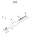
- FIG. 2 an embodiment of a support member 30 according to the invention is shown.
- the electrical substrate 32 on which probe molecules, for example probe nucleic acid oligomers are immobilized in, for example, 96 test sites, is arranged on the carrier section 44 of the carrier element 30.
- the electrical substrate 32 is a biochip, in particular a DNA chip or a protein chip. This biochip is firmly connected to the carrier element 30.
- the illustrated carrier element 30 has conductive regions. These serve to establish an electrical contact between the electrical substrate 32 and a detection and / or evaluation unit (not shown).
- Support element 30 shown comprises an upper holding portion 42, a middle portion 34 and a lower support portion 44, on which the electrical substrate 32 is arranged.
- the support portion 44 has electrical contact pads 48 in electrical contact with the electrical contact pads 36 of the electrical substrate 32.
- the contact points 50 are located laterally on the holding section 42. The contact points 50 make electrical contacts to a subsequent detection and / or evaluation unit.
- the carrier element 30 has a T-structure and a chamfer or widening in the lowest edge region of the carrier section 44.
- conductive areas are provided in the central portion 34, which allow the conduction of the electrical data from the electrical contact points 48 of the support portion 44 to the electrical contact points 50 of the holding portion 42.
- These lines are embedded in the insulating material of the carrier element 30. In this way, a direct detection of events, in particular of hybridization events, at the respective test site is possible.
- the signal transmitted via the conductive connections can be a pure measurement signal which must be further processed by a subsequent detection or evaluation unit.
- CMOS chip in which the measurement signal is evaluated by means of microelectronics integrated in the chip, digital data is transferred between the chip and the evaluation unit, so that the carrier element 30 used must have a smaller number of contact points 50 , In particular, when using active chips only five contact points 50 on the holding portion 42 of the support member 30 are necessary. These are arranged, for example, at the upper end of the holding portion 42.
- a biochip 32 arranged on the carrier section 44 projects relatively far down the lower edge of the carrier element 30 and is significantly narrower than the carrier section 44.
- the test locations 24 and the electrical contact points 36 of the electrical substrate are shown in detail and the electrical contact pads 48 of the carrier portion 44.
- the electrical pads 36 are in electrical contact with the test sites 24 of the electrical substrate 32.
- the electrical pads 48 of the carrier portion 44 are in electrical contact with the electrical pads 36 of the electrical substrate 32.
- the SiO x or SiN x coverlayer electrical substrate (16) is incubated for 1 min to 2 hours at room temperature in a freshly prepared 0.1 to 2% (v / v) solution of trimethylchlorosilane in dry heptane incubated. During this reaction time, the silane is covalently bonded to the surface of the silicon nitride with the release of HCl. Subsequently, the substrate is rinsed twice with silane-free heptane, with ethanol and finally with ultrapure water. Water beading indicates successful hydrophobization.
- the surface may be pre-incubated by plasma treatment or conc. H 2 SO 4/30% H 2 O 2 (in a ratio of 1: 2 (v / v)) to be treated.
- H 2 SO 4/30% H 2 O 2 in a ratio of 1: 2 (v / v)
- other silanes such as dimethyldichlorosilane, propyldimethylchlorosilane, etc. and other solvents such as chloroform, hexane, methylene chloride, etc. may be used.
- the electrical substrate with SiO x or SiN x cover is 15 minutes at room temperature hexamethyldisilazane (HMDS) exposed in the gas phase.
- HMDS hexamethyldisilazane
- This can be accomplished by producing an HMDS-enriched argon or nitrogen atmosphere by passing argon or nitrogen through the liquid HMDS, which is passed into or through the vessel in which the substrates to be coated are located. During this reaction time, a covalent attachment of the trimethylsilyl group takes place with release of NH 3 to the surface of the silicon nitride. Subsequently, HMDS-free argon or nitrogen is passed over the substrate. Water beading indicates successful hydrophobization.
- the surface may be pre-incubated by plasma treatment or conc. H 2 SO 4/30% H 2 O 2 (in a ratio of 1: 2 (v / v)) to be treated.
- any equipment and methods for chemical vapor deposition can be used, as they are used in semiconductor technology and are well known in the art.
Landscapes
- Health & Medical Sciences (AREA)
- Life Sciences & Earth Sciences (AREA)
- Chemical & Material Sciences (AREA)
- Molecular Biology (AREA)
- Physics & Mathematics (AREA)
- Chemical Kinetics & Catalysis (AREA)
- Spectroscopy & Molecular Physics (AREA)
- Electrochemistry (AREA)
- Analytical Chemistry (AREA)
- Biochemistry (AREA)
- General Health & Medical Sciences (AREA)
- General Physics & Mathematics (AREA)
- Immunology (AREA)
- Pathology (AREA)
- Apparatus Associated With Microorganisms And Enzymes (AREA)
Applications Claiming Priority (1)
| Application Number | Priority Date | Filing Date | Title |
|---|---|---|---|
| DE200810002267 DE102008002267B3 (de) | 2008-06-06 | 2008-06-06 | Elektrisches Subtrat zum Einsatz als Träger von Biomolekülen |
Publications (2)
| Publication Number | Publication Date |
|---|---|
| EP2130930A2 true EP2130930A2 (fr) | 2009-12-09 |
| EP2130930A3 EP2130930A3 (fr) | 2014-02-12 |
Family
ID=41110591
Family Applications (1)
| Application Number | Title | Priority Date | Filing Date |
|---|---|---|---|
| EP09161497.4A Withdrawn EP2130930A3 (fr) | 2008-06-06 | 2009-05-29 | Substrat électrique destiné à l'utilisation comme support de biomolécules |
Country Status (2)
| Country | Link |
|---|---|
| EP (1) | EP2130930A3 (fr) |
| DE (1) | DE102008002267B3 (fr) |
Citations (2)
| Publication number | Priority date | Publication date | Assignee | Title |
|---|---|---|---|---|
| WO1999051778A1 (fr) | 1998-04-08 | 1999-10-14 | California Institute Of Technology | Capteur electrochimique utilisant des fractions intercalaires a activite redox |
| WO2003018834A2 (fr) | 2001-08-25 | 2003-03-06 | Friz Biochem Gmbh | Essai de deplacement destine a la detection d'hybridations d'oligomeres d'acide nucleique |
Family Cites Families (7)
| Publication number | Priority date | Publication date | Assignee | Title |
|---|---|---|---|---|
| US5378343A (en) * | 1993-01-11 | 1995-01-03 | Tufts University | Electrode assembly including iridium based mercury ultramicroelectrode array |
| DE19916867A1 (de) * | 1999-04-14 | 2000-10-19 | Fraunhofer Ges Forschung | Anordnung und Verfahren zur Herstellung planarer Arrays mit immobilisierten Molekülen |
| US6623945B1 (en) * | 1999-09-16 | 2003-09-23 | Motorola, Inc. | System and method for microwave cell lysing of small samples |
| DE10331299A1 (de) * | 2003-07-10 | 2005-02-03 | Infineon Technologies Ag | Sensor-Transistor-Element, Sensor-Einheit und Sensor-Array |
| JP4007606B2 (ja) * | 2004-02-03 | 2007-11-14 | キヤノン株式会社 | センサおよび検出方法 |
| DE102004031127A1 (de) * | 2004-06-28 | 2006-01-19 | Infineon Technologies Ag | Biosensor, Verfahren zum Herstellen eines Biosensors und Biosensor-Anordnung |
| US7641777B2 (en) * | 2004-09-07 | 2010-01-05 | Roche Diagnostics Operations, Inc. | Biological testing system |
-
2008
- 2008-06-06 DE DE200810002267 patent/DE102008002267B3/de not_active Expired - Fee Related
-
2009
- 2009-05-29 EP EP09161497.4A patent/EP2130930A3/fr not_active Withdrawn
Patent Citations (2)
| Publication number | Priority date | Publication date | Assignee | Title |
|---|---|---|---|---|
| WO1999051778A1 (fr) | 1998-04-08 | 1999-10-14 | California Institute Of Technology | Capteur electrochimique utilisant des fractions intercalaires a activite redox |
| WO2003018834A2 (fr) | 2001-08-25 | 2003-03-06 | Friz Biochem Gmbh | Essai de deplacement destine a la detection d'hybridations d'oligomeres d'acide nucleique |
Also Published As
| Publication number | Publication date |
|---|---|
| EP2130930A3 (fr) | 2014-02-12 |
| DE102008002267B3 (de) | 2009-11-26 |
Similar Documents
| Publication | Publication Date | Title |
|---|---|---|
| DE60218347T2 (de) | Mesoporöse permeationsschichten zur verwendung an elektronischen aktivmatrixbauelementen | |
| DE69923852T2 (de) | Vorrichtung mit einer vielzahl von analysepunkten auf einer oberfläche und verfahren zur herstellung der vorrichtung | |
| DE69817850T2 (de) | Kovalente immobilisierung mit hoher oberflächendichte von oligonukleotid-monoschichten | |
| EP1171768B1 (fr) | Procede de realisation de systemes de detection avec reseaux plans | |
| EP1786927B1 (fr) | Dispositif et procede de detection de macromolecules chargees | |
| DE602006000939T2 (de) | Nanometervorrichtung zur Messung der Leitfähigkeit und Quanteneffekte einzelner Moleküle sowie Verfahren zur Herstellung und Verwendung | |
| DE10049901C2 (de) | Vorrichtung und Verfahren zur elektrisch beschleunigten Immobilisierung und zur Detektion von Molekülen | |
| EP3004858A2 (fr) | Procécé pour produire une pluralité de zones de mesure sur une puce et puce pourvue de zones de mesure | |
| DE10324912A1 (de) | Verfahren zur Detektion von DNA-Punktmutationen (SNP-Analyse) sowie zugehörige Anordnung | |
| DE112005003134B4 (de) | Elektrisch aktiver kombinatorisch-chemischer (electrically-active combinatorial-chemical; eacc) Chip zur biochemischen Analytbestimmung | |
| EP1573062B1 (fr) | Procede et dispositif d'amplification par pcr et de detection de sequences nucleotidiques | |
| DE102008002267B3 (de) | Elektrisches Subtrat zum Einsatz als Träger von Biomolekülen | |
| EP1573328B1 (fr) | Biopuce | |
| DE10211358B4 (de) | Vertikal-Impedanz-Sensor-Anordnung und Verfahren zum Herstellen einer Vertikal-Impedanz-Sensor-Anordnung | |
| DE102004019357A1 (de) | Verfahren zur Funktionalisierung von Biosensor-Chips | |
| DE29923907U1 (de) | Miniaturisierter Objektträger zur Durchführung einer Vielzahl von Testreihen im Submikroliterbereich | |
| WO2002031482A2 (fr) | Dispositif et procede d'immobilisation acceleree electriquement de molecules | |
| EP1489407A1 (fr) | Méthode et dispositif pour la mesure de la conductivité électronique des substances a analyser avec des marqueurs électro-actifs | |
| WO2003083134A1 (fr) | Detecteur permettant une determination qualitative et quantitative d'oligomeres et polymeres (bio)organiques, procede d'analyse associe et procede de production du detecteur | |
| WO1999042827A2 (fr) | Dispositif de detection d'hybridations d'oligonucleotides et/ou de polynucleotides | |
| DE10256415B3 (de) | Verfahren und Vorrichtung zum Transport bzw. zur bindungspezifischen Trennung elektrisch geladener Moleküle | |
| WO2002094442A1 (fr) | Systeme de distribution sur puce biocapteur et procede pour la distribution d'une solution a distribuer par utilisation de ce systeme de distribution sur une puce biocapteur | |
| Memon et al. | Cephradine-capped gold nanoparticle modified glassy carbon electrode for trace level sensing of triphenyltin hydroxide | |
| DE10312670A1 (de) | Substrat zur kontrollierten Benetzung vorbestimmter Benetzungsstellen mit kleinen Flüssigkeitsvolumina, Substratabdeckung und Flusskammer | |
| DE10320312A1 (de) | Substrat als Träger von Ligaten |
Legal Events
| Date | Code | Title | Description |
|---|---|---|---|
| PUAI | Public reference made under article 153(3) epc to a published international application that has entered the european phase |
Free format text: ORIGINAL CODE: 0009012 |
|
| AK | Designated contracting states |
Kind code of ref document: A2 Designated state(s): AT BE BG CH CY CZ DE DK EE ES FI FR GB GR HR HU IE IS IT LI LT LU LV MC MK MT NL NO PL PT RO SE SI SK TR |
|
| RIC1 | Information provided on ipc code assigned before grant |
Ipc: G01N 27/327 20060101ALI20130918BHEP Ipc: C12Q 1/68 20060101AFI20130918BHEP |
|
| PUAL | Search report despatched |
Free format text: ORIGINAL CODE: 0009013 |
|
| AK | Designated contracting states |
Kind code of ref document: A3 Designated state(s): AT BE BG CH CY CZ DE DK EE ES FI FR GB GR HR HU IE IS IT LI LT LU LV MC MK MT NL NO PL PT RO SE SI SK TR |
|
| AX | Request for extension of the european patent |
Extension state: AL BA RS |
|
| RIC1 | Information provided on ipc code assigned before grant |
Ipc: G01N 27/327 20060101ALI20140106BHEP Ipc: C12Q 1/68 20060101AFI20140106BHEP |
|
| STAA | Information on the status of an ep patent application or granted ep patent |
Free format text: STATUS: THE APPLICATION IS DEEMED TO BE WITHDRAWN |
|
| 18D | Application deemed to be withdrawn |
Effective date: 20140813 |