EP2131483A1 - Geschwindigkeitsregler mit Superkondensator - Google Patents
Geschwindigkeitsregler mit Superkondensator Download PDFInfo
- Publication number
- EP2131483A1 EP2131483A1 EP09161967A EP09161967A EP2131483A1 EP 2131483 A1 EP2131483 A1 EP 2131483A1 EP 09161967 A EP09161967 A EP 09161967A EP 09161967 A EP09161967 A EP 09161967A EP 2131483 A1 EP2131483 A1 EP 2131483A1
- Authority
- EP
- European Patent Office
- Prior art keywords
- bus
- converter
- line
- current
- inductor
- Prior art date
- Legal status (The legal status is an assumption and is not a legal conclusion. Google has not performed a legal analysis and makes no representation as to the accuracy of the status listed.)
- Granted
Links
Images
Classifications
-
- H—ELECTRICITY
- H02—GENERATION; CONVERSION OR DISTRIBUTION OF ELECTRIC POWER
- H02M—APPARATUS FOR CONVERSION BETWEEN AC AND AC, BETWEEN AC AND DC, OR BETWEEN DC AND DC, AND FOR USE WITH MAINS OR SIMILAR POWER SUPPLY SYSTEMS; CONVERSION OF DC OR AC INPUT POWER INTO SURGE OUTPUT POWER; CONTROL OR REGULATION THEREOF
- H02M5/00—Conversion of AC power input into AC power output, e.g. for change of voltage, for change of frequency, for change of number of phases
- H02M5/40—Conversion of AC power input into AC power output, e.g. for change of voltage, for change of frequency, for change of number of phases with intermediate conversion into DC
- H02M5/42—Conversion of AC power input into AC power output, e.g. for change of voltage, for change of frequency, for change of number of phases with intermediate conversion into DC by static converters
- H02M5/44—Conversion of AC power input into AC power output, e.g. for change of voltage, for change of frequency, for change of number of phases with intermediate conversion into DC by static converters using discharge tubes or semiconductor devices to convert the intermediate DC into AC
-
- F—MECHANICAL ENGINEERING; LIGHTING; HEATING; WEAPONS; BLASTING
- F02—COMBUSTION ENGINES; HOT-GAS OR COMBUSTION-PRODUCT ENGINE PLANTS
- F02F—CYLINDERS, PISTONS OR CASINGS, FOR COMBUSTION ENGINES; ARRANGEMENTS OF SEALINGS IN COMBUSTION ENGINES
- F02F3/00—Pistons
- F02F3/02—Pistons having means for accommodating or controlling heat expansion
-
- H—ELECTRICITY
- H02—GENERATION; CONVERSION OR DISTRIBUTION OF ELECTRIC POWER
- H02P—CONTROL OR REGULATION OF ELECTRIC MOTORS, ELECTRIC GENERATORS OR DYNAMO-ELECTRIC CONVERTERS; CONTROLLING TRANSFORMERS, REACTORS OR CHOKE COILS
- H02P3/00—Arrangements for stopping or slowing electric motors, generators, or dynamo-electric converters
- H02P3/02—Details of stopping control
-
- F—MECHANICAL ENGINEERING; LIGHTING; HEATING; WEAPONS; BLASTING
- F02—COMBUSTION ENGINES; HOT-GAS OR COMBUSTION-PRODUCT ENGINE PLANTS
- F02F—CYLINDERS, PISTONS OR CASINGS, FOR COMBUSTION ENGINES; ARRANGEMENTS OF SEALINGS IN COMBUSTION ENGINES
- F02F1/00—Cylinders; Cylinder heads
Definitions
- the present invention relates to a variable speed drive comprising means for storing the energy generated during a braking of the electric charge.
- These storage means are for example in the form of one or more supercapacitors, also called super-capacitors or ultra-capacitors.
- a variable speed drive is connected to the power supply network and intended to control an electrical load. It comprises as input a voltage rectifier module which generates a DC voltage from an AC voltage supplied by the network and which feeds downstream a DC power bus having a positive line and a negative line. A filter capacitor, commonly referred to as a bus capacitor, is mounted between a positive line and a negative line of the DC bus.
- the drive comprises an inverter module powered by the DC bus, making it possible to generate, from the DC voltage, a variable voltage which can be of variable amplitude and frequency by using electronic switches, for example of the IGBT transistor type. controlled by Pulse Width Modulation (PWM or PWM).
- PWM Pulse Width Modulation
- This type of device described in the prior art thus makes it possible to store the braking energy, to provide energy at the start of the load, to compensate for voltage dips and to fill a power supply function over a short period of time. without interruption (called UPS for "Uninterruptible Power Supply”).
- UPS Uninterruptible Power Supply
- This type of device has the advantage of being particularly simple, robust and to be perfectly compatible with single- or three-phase power supply networks.
- THDI disortion rate in current
- the object of the invention is to propose a speed variator enabling the functions of the device of the prior art to be fulfilled and in which the input THDI at the input of the variator is reduced.
- the device for transforming the voltage source constituted by the bus capacitor into a current source is a first inductance.
- the drive further includes a second inductor connected in series with the first inductor. This second inductor is connected in series with the first inductor on the positive or negative line of the DC bus, the DC / DC converter being connected to the corresponding line of the DC bus between the first inductor and the second inductor.
- the measuring means are placed upstream or downstream of the connection point of the DC / DC converter on the line of the DC bus carrying the first inductor.
- the DC / DC converter comprises two electronic switches in series mounted between the positive line and the negative line of the DC bus and a capacitor connected in parallel and upstream of the two switches.
- the electronic switches of the DC / DC converter are for example of the IGBT type.
- the drive comprises a third inductor connected between the midpoint formed by the two electronic switches of the DC / DC converter and a terminal of the energy storage means.
- the variator also comprises means for measuring the current flowing through the energy storage means.
- the drive comprises a switch mounted upstream of the DC / DC converter, on a conductive line connecting the DC / DC converter to the DC bus.
- control module comprises an external loop controlling an internal current loop for controlling the DC / DC converter.
- the energy storage means comprise one or more supercapacitors.
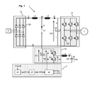
- a variable speed drive 1 comprises an input rectifier module 12 which is intended to rectify an AC three-phase voltage from an external power supply network A (for example a three-phase 380Vac electrical network).
- This rectifier module 12 advantageously uses diodes 120 which are more economical and more reliable than thyristors.
- This rectified voltage can be filtered to obtain a DC voltage Vdc (for example of the order of 200 to 800Vcc or more, depending on the conditions of use) applied to a DC power supply bus composed of a positive line 10 and a negative line 11.
- a capacitor Cb bus is usually used to keep constant the voltage Vdc of the DC bus.
- This bus capacitor Cb is connected between the positive line 10 and the negative line 11 of the bus and is generally of the electrolytic type in standard drives.
- the variable speed drive 1 comprises at the output an inverter module 13 making it possible, from the DC bus, to control an electric load C with a variable voltage which may be of variable amplitude and frequency.
- the inverter module 13 uses for this purpose a Pulse Width Modulation (PWM) control for controlling electronic power switches 130 mounted on each phase. These switches are power transistors, for example of the IGBT type, controlled by a control unit (not shown) producing the PWM.
- PWM Pulse Width Modulation
- the inverter module 13 comprises three arms for supplying a three-phase variable voltage to the electrical load C, each arm being provided with two power transistors 130 in series between a positive terminal and a negative terminal of the power bus, for a total of six power transistors.
- the invention consists in particular in connecting energy storage means between the positive line 10 and the negative line 11 of the DC bus and placing a DC / DC converter 14 (hereinafter DC / DC converter) between the means of energy storage and the continuous bus.
- the energy storage means are for example composed of one or more capacitors, more particularly the super-capacitor type (s) (also called super-capacitance or ultra-capacitance).
- s super-capacitor type
- a super-capacitor behaves like an electrochemical battery in that it is capable of storing a larger volume of electrical energy than a standard capacitor, but unlike an electrochemical battery, it behaves like a standard capacitor in that It is able to withstand high currents of charge and discharge.
- the assembly constituted by the energy storage means (hereinafter super-capacitor UC) and the DC / DC converter 14 is connected, between the positive line 10 and the negative line 11 of the DC bus, in parallel with the capacitor bus, downstream from the rectifier module and upstream with respect to the bus capacitor Cb.
- the DC / DC converter 14 is connected at a point M on the positive line 10 of the DC bus and at a point N on the negative line 11 of the DC bus.
- the DC / DC converter 14 comprises a capacitor C1 and two power transistors T1, T2 in series, for example of the IGBT type.
- the capacitor C1 is connected in parallel with the bus capacitor Cb and in parallel with the two transistors T1, T2 in series.
- the capacitor C1 is a decoupling capacitor forming a switching cell with the transistors T1 and T2. This switching cell must present a parasitic inductance as low as possible to limit the overvoltages related to the switching of the two transistors T1, T2 and not to exceed the maximum voltage that can support the two transistors (600 volts for a network voltage of 200 volts or 1200 volts for a voltage 400 Volt network).
- the capacitance of the capacitor C1 is of low value, for example of the order of a few microfarads so as to filter the commutations.
- an inductor L3 is connected between the midpoint of the two transistors T1 and T2 and a first terminal of the super-capacitor UC.
- the second terminal of the super-capacitor UC is looped back to the free terminal of one of the two transistors T1 or T2.
- the inductor L3 is a smoothing inductor designed to limit the ripple of the current flowing in the supercapacitor UC. This ripple should for example be 15%.
- a device is added in series on the positive line 10 or the negative line 11 of the DC bus, upstream of the bus capacitor Cb and downstream of the connection point M or N of the DC / DC converter 14 on the DC bus.
- This device is for example an inductor L2.
- the inductor L2 is placed on the positive line 10 of the DC bus.
- the inductance L2 makes it possible to naturally reduce the current harmonic distortion rate (hereinafter THDI) to a value between 48% and 80%.
- the inductor L2 also makes it possible to reduce the maximum current to the DC / DC converter and thus to be able to optimize the sizing of the transistors T1, T2 of the DC / DC converter.
- the device making it possible to transform the voltage source constituted by the bus capacitor Cb into a current source may for example be a diode with a switch connected in parallel or a resistor without loss.
- inductor L1 upstream of the capacitor C1 of the DC / DC converter 14.
- This inductance L1 can be placed on the conductive line connecting the capacitor C1 at the connection point M or N (variant not shown) or preferably directly on a line of the DC bus, upstream of the connection point M or N of the DC / DC converter and downstream of the rectifier module.
- Inductors L1 and L2 are connected in series on both sides of the connection point M of the DC / DC converter on the positive bus line continued.
- a switch S1 for example of the contactor type, on one of the conductive lines connecting the capacitor C1 to the connection point M or N on the DC bus.
- This contactor S1 makes it possible to avoid discharging the supercapacitor UC when the voltage Vdc of the DC bus at the output of the rectifier module 12 is less than the voltage Vuc at the terminals of the supercapacitor UC and when the drive is not powered by network A.
- Transistors T1 and T2 are controlled on initiation, that is to say on closing or blocking, that is to say on opening, using a control module 2 modulator type performing a pulse width modulation.
- Pulse width modulation consists of comparing a high frequency carrier with a modulating low frequency or constant. The switching frequency is fixed by the frequency of the carrier and is for example equal to 20 kHz.
- an internal current loop determines the modulator m so as to control the switching of the transistors T1 and T2 and thus control the average current luc crossing the inductance L3.
- an external loop makes it possible to fix the reference luc * of current to be applied to the internal loop of current to regulate the current luc.
- the external loop will be different and the control transistors T1, T2 will therefore also be different.
- the control unit of the variable speed drive indicates to the control module 2 of the DC / DC converter that the operating mode is recovery of energy.
- the external loop implemented is a voltage loop for controlling the voltage Vdc across the bus capacitor.
- the voltage Vdc of the DC bus increases.
- this voltage reaches a threshold value, for example 750 volts, the DC / DC converter 14 is controlled via the internal loop to divert the surplus energy in the supercapacitor UC, while keeping the voltage Vdc of the continuous bus constant. .
- the accumulation of energy in the super-capacitor UC causes an increase in the voltage across the super-capacitor UC.
- the supercapacitor UC is sized to be able to store all the energy supplied by the load C during braking. However, if the voltage across the super-capacitor UC were to be too high, the excess energy would have to be dissipated in a braking resistor to protect the super-capacitor.
- the super-capacitor UC When starting the drive, the super-capacitor UC is used.
- the drive control unit indicates to the control module 2 of the DC / DC converter 14 that the operating mode is motor.
- the supercapacitor UC supplies energy to the load C via the control of the DC / DC converter 14.
- a current setpoint is applied at the input of the internal loop in such a way that to control the flow of current to the load all by ensuring that the voltage Vdc of the DC bus does not exceed a certain threshold, for example set at 700 volts.
- a low threshold for example set at half of its maximum voltage when it is fully charged, the supercapacitor UC is no longer used until it again reaches a sufficient voltage level.
- the voltage Vdc of the continuous bus can decrease until it reaches a low threshold from which the energy stored in the supercapacitor UC is used.
- the current setpoint applied to the DC / DC converter 14 for supplying current is determined from an external voltage loop whose setpoint is to maintain the voltage Vdc of the DC bus at a determined level, for example 700 volts.
- a last mode of operation consists in using the assembly consisting of the DC / DC converter 14 and the supercapacitor UC as a parallel active filter for the DC bus. This consists in controlling the current I1 on the DC bus so that it is constant and thus make it possible to limit the THDI at the input of the rectifier module 12. This mode of operation is used continuously when the motor is running in motor mode thanks to the energy provided by the network.
- a first current sensor placed on the positive line 10 of the DC bus on which the inductances L1 and L2 are positioned and a second current sensor placed in series with the inductance L3 for measuring the current flowing through the inductor are used.
- the first current sensor is placed to measure the current I2 on the positive line of the DC bus downstream of the point M
- the first sensor may be placed to measure the current I1 on the line. positive 10 of the DC bus, upstream of the point M.
- the inductor L2 was placed on the negative line 11 of the bus, the first sensor would be placed on the negative line 11 of the bus, upstream or downstream of the point N.
- the first current sensor may be replaced by software means for estimating the current I1 or I2 flowing upstream of the point M or the point N or downstream of the point M or the point N.
- the measurement of the current I1 or that of the current I2 is filtered in order to keep only the AC component of the measured current I1 or I2.
- the current I2 is composed of a continuous active component proportional to the active power absorbed by the load C and an image reactive component image of a fluctuating reactive power between the network and the drive due to the charge and discharge of the capacitor Cb .
- the goal of the command is then to supply a current I3 equal to the AC reactive component of the current I2 in order to eliminate the AC component of the current I1 and to obtain a constant current.
- the alternative component extracted from the measurements of the currents I1 or I2 is thus applied as current setpoint I3 * to the external loop 21 in order to determine a current setpoint luc * to be applied to the inner loop 22.
- the setpoint I3 * corresponds to the current to be supplied by the super-capacitor UC to eliminate any AC component of the current I1 and thus obtain a constant current I1 at the output of the rectifier module 13 and thus a THDI at the input of the low drive.
- the current set point Iuc * will be different.
- the current setpoint Iuc * is calculated by applying a constant power calculation, that is to say that the input power of the DC / DC converter is equal to the output power of the DC converter / DC.
- the setpoint Iuc * obtained can therefore be applied to the inner loop 22 in order to control the transistors T1 and T2 so as to control the current luc passing through the supercapacitor UC.
- the current luc that is to say the current flowing through the inductance L3 and the supercapacitor UC
- a gain can be applied to the setpoint Iuc * at the input of the inner loop 22 when the measured current is I1.
- control of the transistors T1, T2 of the DC / DC converter 14 must be adapted to take account of the decrease of the voltage Vuc across the super-capacitor UC due to the losses generated during the switching of the transistors T1, T2. In the inner loop 22, the voltage Vuc must therefore be measured and monitored to be kept constant.
Landscapes
- Engineering & Computer Science (AREA)
- Power Engineering (AREA)
- Chemical & Material Sciences (AREA)
- Combustion & Propulsion (AREA)
- Mechanical Engineering (AREA)
- General Engineering & Computer Science (AREA)
- Inverter Devices (AREA)
- Control Of Ac Motors In General (AREA)
- Control Of Electric Motors In General (AREA)
- Dc-Dc Converters (AREA)
Applications Claiming Priority (1)
| Application Number | Priority Date | Filing Date | Title |
|---|---|---|---|
| FR0853722A FR2932327B1 (fr) | 2008-06-05 | 2008-06-05 | Variateur de vitesse avec super-condensateur |
Publications (2)
| Publication Number | Publication Date |
|---|---|
| EP2131483A1 true EP2131483A1 (de) | 2009-12-09 |
| EP2131483B1 EP2131483B1 (de) | 2011-09-07 |
Family
ID=40303506
Family Applications (1)
| Application Number | Title | Priority Date | Filing Date |
|---|---|---|---|
| EP09161967A Active EP2131483B1 (de) | 2008-06-05 | 2009-06-04 | Geschwindigkeitsregler mit Superkondensator |
Country Status (4)
| Country | Link |
|---|---|
| EP (1) | EP2131483B1 (de) |
| AT (1) | ATE523953T1 (de) |
| ES (1) | ES2367950T3 (de) |
| FR (1) | FR2932327B1 (de) |
Cited By (1)
| Publication number | Priority date | Publication date | Assignee | Title |
|---|---|---|---|---|
| WO2012065806A1 (fr) | 2010-11-15 | 2012-05-24 | Schneider Toshiba Inverter Europe Sas | Variateur de vitesse dote d'un module a super-condensateurs |
Citations (3)
| Publication number | Priority date | Publication date | Assignee | Title |
|---|---|---|---|---|
| US20030089557A1 (en) * | 2000-03-31 | 2003-05-15 | Thomas Eilinger | Device and method for reducing the power of the supply connection in lift systems |
| JP2006087299A (ja) * | 2005-11-04 | 2006-03-30 | Toshiba Corp | 電気車制御装置 |
| EP1833158A2 (de) * | 2006-03-10 | 2007-09-12 | Deere & Company | Verfahren und System zum Verwalten der Stromabgabe eines Turbogenerators |
-
2008
- 2008-06-05 FR FR0853722A patent/FR2932327B1/fr not_active Expired - Fee Related
-
2009
- 2009-06-04 AT AT09161967T patent/ATE523953T1/de not_active IP Right Cessation
- 2009-06-04 ES ES09161967T patent/ES2367950T3/es active Active
- 2009-06-04 EP EP09161967A patent/EP2131483B1/de active Active
Patent Citations (4)
| Publication number | Priority date | Publication date | Assignee | Title |
|---|---|---|---|---|
| US20030089557A1 (en) * | 2000-03-31 | 2003-05-15 | Thomas Eilinger | Device and method for reducing the power of the supply connection in lift systems |
| US6742630B2 (en) | 2000-03-31 | 2004-06-01 | Inventio Ag | Super-capacitor energy storage unit for elevator installations |
| JP2006087299A (ja) * | 2005-11-04 | 2006-03-30 | Toshiba Corp | 電気車制御装置 |
| EP1833158A2 (de) * | 2006-03-10 | 2007-09-12 | Deere & Company | Verfahren und System zum Verwalten der Stromabgabe eines Turbogenerators |
Non-Patent Citations (5)
| Title |
|---|
| CHUNG-PING CHEN ET AL: "Error bounded Pade approximation via bilinear conformal transformation", DESIGN AUTOMATION CONFERENCE, 1999. PROCEEDINGS. 36TH NEW ORLEANS, LA, USA 21-25 JUNE 1999, PISCATAWAY, NJ, USA,IEEE, US, 21 June 1999 (1999-06-21), pages 7 - 12, XP010344048, ISBN: 978-1-58113-092-8 * |
| CHUNG-PING CHEN ET AL: "Error Bounded Padé Approximation via Bilinear Conformal Transformation", DESIGN AUTOMATION, 1999. 36TH ANNUAL CONFERENCE ON NEW ORLEANS, LA, USA 21-25 JUNE 1999, PISCATAWAY, NJ, USA,IEEE, 21 June 1999 (1999-06-21), pages 7 - 12, XP010762051, ISBN: 978-1-58113-109-3 * |
| NONAKA S ET AL: "Single-phase PWM current source converter with double-frequency parallel resonance circuit for DC smoothing", INDUSTRY APPLICATIONS SOCIETY ANNUAL MEETING, 1993., CONFERENCE RECORD OF THE 1993 IEEE TORONTO, ONT., CANADA 2-8 OCT. 1993, NEW YORK, NY, USA,IEEE, US, 2 October 1993 (1993-10-02), pages 1144 - 1151, XP010118825, ISBN: 978-0-7803-1462-7 * |
| SRAJBER D: "How to find the best solution for power converters and for the new principle of operation", 19930101, 1 January 1993 (1993-01-01), pages 246 - 249, XP006511470 * |
| TEULINGS W ET AL: "Analysis of the current distribution between paralleled capacitors in a chopper on printed circuit board", INDUSTRY APPLICATIONS CONFERENCE, 1997. THIRTY-SECOND IAS ANNUAL MEETI NG, IAS '97., CONFERENCE RECORD OF THE 1997 IEEE NEW ORLEANS, LA, USA 5-9 OCT. 1997, NEW YORK, NY, USA,IEEE, US, vol. 2, 5 October 1997 (1997-10-05), pages 1066 - 1072, XP010248464, ISBN: 978-0-7803-4067-1 * |
Cited By (1)
| Publication number | Priority date | Publication date | Assignee | Title |
|---|---|---|---|---|
| WO2012065806A1 (fr) | 2010-11-15 | 2012-05-24 | Schneider Toshiba Inverter Europe Sas | Variateur de vitesse dote d'un module a super-condensateurs |
Also Published As
| Publication number | Publication date |
|---|---|
| EP2131483B1 (de) | 2011-09-07 |
| ES2367950T3 (es) | 2011-11-11 |
| FR2932327A1 (fr) | 2009-12-11 |
| ATE523953T1 (de) | 2011-09-15 |
| FR2932327B1 (fr) | 2010-06-04 |
Similar Documents
| Publication | Publication Date | Title |
|---|---|---|
| EP1788697B1 (de) | Gerät zur Korrektur des Leistungsfaktors für einen drehzahlgeregelten Antrieb | |
| EP3554887B1 (de) | Steuerungsverfahren einer in einem elektrischen oder hybriden fahrzeug eingebetteten ladevorrichtung | |
| EP2859651B1 (de) | Absorptionsschaltung zur absorption einer stromwelle und zugehöriges verfahren | |
| EP2338225B1 (de) | Energiewiedergewinnungseinrichtung in einem antrieb mit variabler frequenz | |
| EP2641323B1 (de) | Drehzahlvariabler antrieb mit superkondensatormodul | |
| FR3048830A1 (fr) | Procede et dispositif de commande en monophase d'un chargeur de vehicules a traction electrique ou hybride embarque sans isolation galvanique | |
| EP3320593B1 (de) | System zur energieerzeugung mit verbesserter behandlung von laststössen, lastabwürfen und oberschwingungen | |
| EP2281337B1 (de) | Verfahren zur energierückgewinnung in einem drehzahl variablen antrieb | |
| EP3807985B1 (de) | Wechselstrom-gleichstrom-wandler | |
| EP2595291B1 (de) | Leistungswandler, der mit mehreren Stromquellen ausgestattet ist, die parallel gesteuert und verbunden sind | |
| FR2990078A1 (fr) | Procede de commande de charge d'une batterie | |
| EP3707815B1 (de) | Verfahren zur steuerung eines dreiphasigen vienna-gleichrichters bei fehlerhaftem leistungsschalter | |
| EP2815493B1 (de) | Elektrische ac/dc-umwandlungsvorrichtung zur energierückgewinnung und verwaltung von gleichstromseitigen kurzschlüssen und steuerverfahren einer solchen vorrichtung | |
| EP3539204B1 (de) | Verfahren zur steuerung eines dreiphasigen gleichrichters für eine ladevorrichtung an bord eines elektro- oder hybridfahrzeugs | |
| EP3520210B1 (de) | Verfahren zur steuerung eines dreiphasigen wechselrichters für eine ladevorrichtung an bord eines elektro- oder hybridfahrzeugs | |
| WO2014053557A1 (fr) | Regulation d'un module electronique adaptateur de tension | |
| EP3539203B1 (de) | Verfahren zur steuerung eines dreiphasigen wechselrichters für eine ladevorrichtung an bord eines elektro- oder hybridfahrzeugs | |
| EP2131483B1 (de) | Geschwindigkeitsregler mit Superkondensator | |
| EP3685485B1 (de) | Verfahren zur steuerung eines ladesystems einer traktionbatterie | |
| FR3082678A1 (fr) | Procede de commande d'un redresseur de vienne. |
Legal Events
| Date | Code | Title | Description |
|---|---|---|---|
| PUAI | Public reference made under article 153(3) epc to a published international application that has entered the european phase |
Free format text: ORIGINAL CODE: 0009012 |
|
| AK | Designated contracting states |
Kind code of ref document: A1 Designated state(s): AT BE BG CH CY CZ DE DK EE ES FI FR GB GR HR HU IE IS IT LI LT LU LV MC MK MT NL NO PL PT RO SE SI SK TR |
|
| 17P | Request for examination filed |
Effective date: 20100108 |
|
| 17Q | First examination report despatched |
Effective date: 20100201 |
|
| GRAP | Despatch of communication of intention to grant a patent |
Free format text: ORIGINAL CODE: EPIDOSNIGR1 |
|
| GRAS | Grant fee paid |
Free format text: ORIGINAL CODE: EPIDOSNIGR3 |
|
| GRAA | (expected) grant |
Free format text: ORIGINAL CODE: 0009210 |
|
| REG | Reference to a national code |
Ref country code: GB Ref legal event code: FG4D Free format text: NOT ENGLISH |
|
| REG | Reference to a national code |
Ref country code: CH Ref legal event code: EP |
|
| REG | Reference to a national code |
Ref country code: IE Ref legal event code: FG4D Free format text: LANGUAGE OF EP DOCUMENT: FRENCH |
|
| REG | Reference to a national code |
Ref country code: ES Ref legal event code: FG2A Ref document number: 2367950 Country of ref document: ES Kind code of ref document: T3 Effective date: 20111111 |
|
| REG | Reference to a national code |
Ref country code: DE Ref legal event code: R096 Ref document number: 602009002522 Country of ref document: DE Effective date: 20111201 |
|
| REG | Reference to a national code |
Ref country code: NL Ref legal event code: VDEP Effective date: 20110907 |
|
| PG25 | Lapsed in a contracting state [announced via postgrant information from national office to epo] |
Ref country code: NO Free format text: LAPSE BECAUSE OF FAILURE TO SUBMIT A TRANSLATION OF THE DESCRIPTION OR TO PAY THE FEE WITHIN THE PRESCRIBED TIME-LIMIT Effective date: 20111207 Ref country code: SE Free format text: LAPSE BECAUSE OF FAILURE TO SUBMIT A TRANSLATION OF THE DESCRIPTION OR TO PAY THE FEE WITHIN THE PRESCRIBED TIME-LIMIT Effective date: 20110907 Ref country code: FI Free format text: LAPSE BECAUSE OF FAILURE TO SUBMIT A TRANSLATION OF THE DESCRIPTION OR TO PAY THE FEE WITHIN THE PRESCRIBED TIME-LIMIT Effective date: 20110907 Ref country code: HR Free format text: LAPSE BECAUSE OF FAILURE TO SUBMIT A TRANSLATION OF THE DESCRIPTION OR TO PAY THE FEE WITHIN THE PRESCRIBED TIME-LIMIT Effective date: 20110907 Ref country code: LT Free format text: LAPSE BECAUSE OF FAILURE TO SUBMIT A TRANSLATION OF THE DESCRIPTION OR TO PAY THE FEE WITHIN THE PRESCRIBED TIME-LIMIT Effective date: 20110907 |
|
| LTIE | Lt: invalidation of european patent or patent extension |
Effective date: 20110907 |
|
| PG25 | Lapsed in a contracting state [announced via postgrant information from national office to epo] |
Ref country code: LV Free format text: LAPSE BECAUSE OF FAILURE TO SUBMIT A TRANSLATION OF THE DESCRIPTION OR TO PAY THE FEE WITHIN THE PRESCRIBED TIME-LIMIT Effective date: 20110907 Ref country code: SI Free format text: LAPSE BECAUSE OF FAILURE TO SUBMIT A TRANSLATION OF THE DESCRIPTION OR TO PAY THE FEE WITHIN THE PRESCRIBED TIME-LIMIT Effective date: 20110907 Ref country code: GR Free format text: LAPSE BECAUSE OF FAILURE TO SUBMIT A TRANSLATION OF THE DESCRIPTION OR TO PAY THE FEE WITHIN THE PRESCRIBED TIME-LIMIT Effective date: 20111208 Ref country code: CY Free format text: LAPSE BECAUSE OF FAILURE TO SUBMIT A TRANSLATION OF THE DESCRIPTION OR TO PAY THE FEE WITHIN THE PRESCRIBED TIME-LIMIT Effective date: 20110907 Ref country code: AT Free format text: LAPSE BECAUSE OF FAILURE TO SUBMIT A TRANSLATION OF THE DESCRIPTION OR TO PAY THE FEE WITHIN THE PRESCRIBED TIME-LIMIT Effective date: 20110907 |
|
| REG | Reference to a national code |
Ref country code: AT Ref legal event code: MK05 Ref document number: 523953 Country of ref document: AT Kind code of ref document: T Effective date: 20110907 |
|
| REG | Reference to a national code |
Ref country code: IE Ref legal event code: FD4D |
|
| PG25 | Lapsed in a contracting state [announced via postgrant information from national office to epo] |
Ref country code: SK Free format text: LAPSE BECAUSE OF FAILURE TO SUBMIT A TRANSLATION OF THE DESCRIPTION OR TO PAY THE FEE WITHIN THE PRESCRIBED TIME-LIMIT Effective date: 20110907 Ref country code: IS Free format text: LAPSE BECAUSE OF FAILURE TO SUBMIT A TRANSLATION OF THE DESCRIPTION OR TO PAY THE FEE WITHIN THE PRESCRIBED TIME-LIMIT Effective date: 20120107 Ref country code: IE Free format text: LAPSE BECAUSE OF FAILURE TO SUBMIT A TRANSLATION OF THE DESCRIPTION OR TO PAY THE FEE WITHIN THE PRESCRIBED TIME-LIMIT Effective date: 20110907 Ref country code: CZ Free format text: LAPSE BECAUSE OF FAILURE TO SUBMIT A TRANSLATION OF THE DESCRIPTION OR TO PAY THE FEE WITHIN THE PRESCRIBED TIME-LIMIT Effective date: 20110907 |
|
| PG25 | Lapsed in a contracting state [announced via postgrant information from national office to epo] |
Ref country code: PL Free format text: LAPSE BECAUSE OF FAILURE TO SUBMIT A TRANSLATION OF THE DESCRIPTION OR TO PAY THE FEE WITHIN THE PRESCRIBED TIME-LIMIT Effective date: 20110907 Ref country code: EE Free format text: LAPSE BECAUSE OF FAILURE TO SUBMIT A TRANSLATION OF THE DESCRIPTION OR TO PAY THE FEE WITHIN THE PRESCRIBED TIME-LIMIT Effective date: 20110907 Ref country code: NL Free format text: LAPSE BECAUSE OF FAILURE TO SUBMIT A TRANSLATION OF THE DESCRIPTION OR TO PAY THE FEE WITHIN THE PRESCRIBED TIME-LIMIT Effective date: 20110907 Ref country code: PT Free format text: LAPSE BECAUSE OF FAILURE TO SUBMIT A TRANSLATION OF THE DESCRIPTION OR TO PAY THE FEE WITHIN THE PRESCRIBED TIME-LIMIT Effective date: 20120109 Ref country code: RO Free format text: LAPSE BECAUSE OF FAILURE TO SUBMIT A TRANSLATION OF THE DESCRIPTION OR TO PAY THE FEE WITHIN THE PRESCRIBED TIME-LIMIT Effective date: 20110907 |
|
| PLBE | No opposition filed within time limit |
Free format text: ORIGINAL CODE: 0009261 |
|
| STAA | Information on the status of an ep patent application or granted ep patent |
Free format text: STATUS: NO OPPOSITION FILED WITHIN TIME LIMIT |
|
| PG25 | Lapsed in a contracting state [announced via postgrant information from national office to epo] |
Ref country code: DK Free format text: LAPSE BECAUSE OF FAILURE TO SUBMIT A TRANSLATION OF THE DESCRIPTION OR TO PAY THE FEE WITHIN THE PRESCRIBED TIME-LIMIT Effective date: 20110907 |
|
| 26N | No opposition filed |
Effective date: 20120611 |
|
| REG | Reference to a national code |
Ref country code: DE Ref legal event code: R097 Ref document number: 602009002522 Country of ref document: DE Effective date: 20120611 |
|
| BERE | Be: lapsed |
Owner name: SCHNEIDER TOSHIBA INVERTER EUROPE SAS Effective date: 20120630 |
|
| PG25 | Lapsed in a contracting state [announced via postgrant information from national office to epo] |
Ref country code: MC Free format text: LAPSE BECAUSE OF NON-PAYMENT OF DUE FEES Effective date: 20120630 |
|
| PG25 | Lapsed in a contracting state [announced via postgrant information from national office to epo] |
Ref country code: MK Free format text: LAPSE BECAUSE OF FAILURE TO SUBMIT A TRANSLATION OF THE DESCRIPTION OR TO PAY THE FEE WITHIN THE PRESCRIBED TIME-LIMIT Effective date: 20110907 |
|
| PG25 | Lapsed in a contracting state [announced via postgrant information from national office to epo] |
Ref country code: BE Free format text: LAPSE BECAUSE OF NON-PAYMENT OF DUE FEES Effective date: 20120630 |
|
| PG25 | Lapsed in a contracting state [announced via postgrant information from national office to epo] |
Ref country code: BG Free format text: LAPSE BECAUSE OF FAILURE TO SUBMIT A TRANSLATION OF THE DESCRIPTION OR TO PAY THE FEE WITHIN THE PRESCRIBED TIME-LIMIT Effective date: 20111207 |
|
| PG25 | Lapsed in a contracting state [announced via postgrant information from national office to epo] |
Ref country code: MT Free format text: LAPSE BECAUSE OF FAILURE TO SUBMIT A TRANSLATION OF THE DESCRIPTION OR TO PAY THE FEE WITHIN THE PRESCRIBED TIME-LIMIT Effective date: 20110907 |
|
| PG25 | Lapsed in a contracting state [announced via postgrant information from national office to epo] |
Ref country code: LU Free format text: LAPSE BECAUSE OF NON-PAYMENT OF DUE FEES Effective date: 20120604 |
|
| PG25 | Lapsed in a contracting state [announced via postgrant information from national office to epo] |
Ref country code: HU Free format text: LAPSE BECAUSE OF FAILURE TO SUBMIT A TRANSLATION OF THE DESCRIPTION OR TO PAY THE FEE WITHIN THE PRESCRIBED TIME-LIMIT Effective date: 20090604 |
|
| REG | Reference to a national code |
Ref country code: FR Ref legal event code: PLFP Year of fee payment: 8 |
|
| REG | Reference to a national code |
Ref country code: FR Ref legal event code: PLFP Year of fee payment: 9 |
|
| REG | Reference to a national code |
Ref country code: FR Ref legal event code: PLFP Year of fee payment: 10 |
|
| PGFP | Annual fee paid to national office [announced via postgrant information from national office to epo] |
Ref country code: GB Payment date: 20240618 Year of fee payment: 16 |
|
| PGFP | Annual fee paid to national office [announced via postgrant information from national office to epo] |
Ref country code: DE Payment date: 20240627 Year of fee payment: 16 |
|
| PGFP | Annual fee paid to national office [announced via postgrant information from national office to epo] |
Ref country code: FR Payment date: 20240625 Year of fee payment: 16 |
|
| PGFP | Annual fee paid to national office [announced via postgrant information from national office to epo] |
Ref country code: TR Payment date: 20240523 Year of fee payment: 16 |
|
| PGFP | Annual fee paid to national office [announced via postgrant information from national office to epo] |
Ref country code: IT Payment date: 20240619 Year of fee payment: 16 |
|
| PGFP | Annual fee paid to national office [announced via postgrant information from national office to epo] |
Ref country code: ES Payment date: 20240710 Year of fee payment: 16 Ref country code: CH Payment date: 20240701 Year of fee payment: 16 |
|
| REG | Reference to a national code |
Ref country code: DE Ref legal event code: R119 Ref document number: 602009002522 Country of ref document: DE |
|
| REG | Reference to a national code |
Ref country code: CH Ref legal event code: H13 Free format text: ST27 STATUS EVENT CODE: U-0-0-H10-H13 (AS PROVIDED BY THE NATIONAL OFFICE) Effective date: 20260127 |
|
| GBPC | Gb: european patent ceased through non-payment of renewal fee |
Effective date: 20250604 |
|
| PG25 | Lapsed in a contracting state [announced via postgrant information from national office to epo] |
Ref country code: GB Free format text: LAPSE BECAUSE OF NON-PAYMENT OF DUE FEES Effective date: 20250604 |
|
| PG25 | Lapsed in a contracting state [announced via postgrant information from national office to epo] |
Ref country code: DE Free format text: LAPSE BECAUSE OF NON-PAYMENT OF DUE FEES Effective date: 20260101 |
|
| PG25 | Lapsed in a contracting state [announced via postgrant information from national office to epo] |
Ref country code: IT Free format text: LAPSE BECAUSE OF NON-PAYMENT OF DUE FEES Effective date: 20250604 |
|
| PG25 | Lapsed in a contracting state [announced via postgrant information from national office to epo] |
Ref country code: FR Free format text: LAPSE BECAUSE OF NON-PAYMENT OF DUE FEES Effective date: 20250630 |
|
| PG25 | Lapsed in a contracting state [announced via postgrant information from national office to epo] |
Ref country code: CH Free format text: LAPSE BECAUSE OF NON-PAYMENT OF DUE FEES Effective date: 20250630 |