EP2133727A1 - Optische Vorrichtung und virtuelle Bildanzeige - Google Patents
Optische Vorrichtung und virtuelle Bildanzeige Download PDFInfo
- Publication number
- EP2133727A1 EP2133727A1 EP09006129A EP09006129A EP2133727A1 EP 2133727 A1 EP2133727 A1 EP 2133727A1 EP 09006129 A EP09006129 A EP 09006129A EP 09006129 A EP09006129 A EP 09006129A EP 2133727 A1 EP2133727 A1 EP 2133727A1
- Authority
- EP
- European Patent Office
- Prior art keywords
- guide plate
- light beams
- light guide
- kinds
- parallel light
- Prior art date
- Legal status (The legal status is an assumption and is not a legal conclusion. Google has not performed a legal analysis and makes no representation as to the accuracy of the status listed.)
- Granted
Links
Images




Classifications
-
- G—PHYSICS
- G02—OPTICS
- G02B—OPTICAL ELEMENTS, SYSTEMS OR APPARATUS
- G02B27/00—Optical systems or apparatus not provided for by any of the groups G02B1/00 - G02B26/00, G02B30/00
- G02B27/01—Head-up displays
- G02B27/017—Head mounted
- G02B27/0172—Head mounted characterised by optical features
-
- G—PHYSICS
- G02—OPTICS
- G02B—OPTICAL ELEMENTS, SYSTEMS OR APPARATUS
- G02B27/00—Optical systems or apparatus not provided for by any of the groups G02B1/00 - G02B26/00, G02B30/00
- G02B27/0081—Optical systems or apparatus not provided for by any of the groups G02B1/00 - G02B26/00, G02B30/00 with means for altering, e.g. enlarging, the entrance or exit pupil
-
- G—PHYSICS
- G02—OPTICS
- G02B—OPTICAL ELEMENTS, SYSTEMS OR APPARATUS
- G02B5/00—Optical elements other than lenses
- G02B5/20—Filters
- G02B5/203—Filters having holographic or diffractive elements
-
- G—PHYSICS
- G02—OPTICS
- G02B—OPTICAL ELEMENTS, SYSTEMS OR APPARATUS
- G02B5/00—Optical elements other than lenses
- G02B5/32—Holograms used as optical elements
-
- G—PHYSICS
- G02—OPTICS
- G02B—OPTICAL ELEMENTS, SYSTEMS OR APPARATUS
- G02B6/00—Light guides; Structural details of arrangements comprising light guides and other optical elements, e.g. couplings
- G02B6/10—Light guides; Structural details of arrangements comprising light guides and other optical elements, e.g. couplings of the optical waveguide type
- G02B6/12—Light guides; Structural details of arrangements comprising light guides and other optical elements, e.g. couplings of the optical waveguide type of the integrated circuit kind
- G02B6/122—Basic optical elements, e.g. light-guiding paths
- G02B6/124—Geodesic lenses or integrated gratings
-
- G—PHYSICS
- G03—PHOTOGRAPHY; CINEMATOGRAPHY; ANALOGOUS TECHNIQUES USING WAVES OTHER THAN OPTICAL WAVES; ELECTROGRAPHY; HOLOGRAPHY
- G03H—HOLOGRAPHIC PROCESSES OR APPARATUS
- G03H1/00—Holographic processes or apparatus using light, infrared or ultraviolet waves for obtaining holograms or for obtaining an image from them; Details peculiar thereto
- G03H1/04—Processes or apparatus for producing holograms
-
- G—PHYSICS
- G02—OPTICS
- G02B—OPTICAL ELEMENTS, SYSTEMS OR APPARATUS
- G02B27/00—Optical systems or apparatus not provided for by any of the groups G02B1/00 - G02B26/00, G02B30/00
- G02B27/01—Head-up displays
- G02B27/0101—Head-up displays characterised by optical features
- G02B2027/011—Head-up displays characterised by optical features comprising device for correcting geometrical aberrations, distortion
-
- G—PHYSICS
- G02—OPTICS
- G02B—OPTICAL ELEMENTS, SYSTEMS OR APPARATUS
- G02B27/00—Optical systems or apparatus not provided for by any of the groups G02B1/00 - G02B26/00, G02B30/00
- G02B27/01—Head-up displays
- G02B27/0101—Head-up displays characterised by optical features
- G02B2027/0112—Head-up displays characterised by optical features comprising device for genereting colour display
-
- G—PHYSICS
- G02—OPTICS
- G02B—OPTICAL ELEMENTS, SYSTEMS OR APPARATUS
- G02B27/00—Optical systems or apparatus not provided for by any of the groups G02B1/00 - G02B26/00, G02B30/00
- G02B27/01—Head-up displays
- G02B27/0101—Head-up displays characterised by optical features
- G02B2027/0112—Head-up displays characterised by optical features comprising device for genereting colour display
- G02B2027/0116—Head-up displays characterised by optical features comprising device for genereting colour display comprising devices for correcting chromatic aberration
-
- G—PHYSICS
- G02—OPTICS
- G02B—OPTICAL ELEMENTS, SYSTEMS OR APPARATUS
- G02B27/00—Optical systems or apparatus not provided for by any of the groups G02B1/00 - G02B26/00, G02B30/00
- G02B27/01—Head-up displays
- G02B27/0101—Head-up displays characterised by optical features
- G02B2027/0118—Head-up displays characterised by optical features comprising devices for improving the contrast of the display / brillance control visibility
-
- G—PHYSICS
- G02—OPTICS
- G02B—OPTICAL ELEMENTS, SYSTEMS OR APPARATUS
- G02B27/00—Optical systems or apparatus not provided for by any of the groups G02B1/00 - G02B26/00, G02B30/00
- G02B27/01—Head-up displays
- G02B27/0101—Head-up displays characterised by optical features
- G02B2027/0123—Head-up displays characterised by optical features comprising devices increasing the field of view
- G02B2027/0125—Field-of-view increase by wavefront division
-
- G—PHYSICS
- G02—OPTICS
- G02B—OPTICAL ELEMENTS, SYSTEMS OR APPARATUS
- G02B27/00—Optical systems or apparatus not provided for by any of the groups G02B1/00 - G02B26/00, G02B30/00
- G02B27/01—Head-up displays
- G02B27/017—Head mounted
- G02B27/0172—Head mounted characterised by optical features
- G02B2027/0174—Head mounted characterised by optical features holographic
-
- G—PHYSICS
- G02—OPTICS
- G02B—OPTICAL ELEMENTS, SYSTEMS OR APPARATUS
- G02B6/00—Light guides; Structural details of arrangements comprising light guides and other optical elements, e.g. couplings
-
- G—PHYSICS
- G03—PHOTOGRAPHY; CINEMATOGRAPHY; ANALOGOUS TECHNIQUES USING WAVES OTHER THAN OPTICAL WAVES; ELECTROGRAPHY; HOLOGRAPHY
- G03H—HOLOGRAPHIC PROCESSES OR APPARATUS
- G03H1/00—Holographic processes or apparatus using light, infrared or ultraviolet waves for obtaining holograms or for obtaining an image from them; Details peculiar thereto
- G03H1/04—Processes or apparatus for producing holograms
- G03H1/0402—Recording geometries or arrangements
- G03H1/0408—Total internal reflection [TIR] holograms, e.g. edge lit or substrate mode holograms
Definitions
- the present invention relates to an optical device and a virtual image display for guiding display image light as a virtual image to viewer's pupils through the use of a reflection type volume hologram grating.
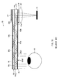
- FIG. 18 illustrates a configuration example of a virtual image display 80 proposed by International Publication No. 2005/093493 pamphlet.
- the virtual image display 80 includes an image display element 81 displaying an image, and a virtual image optical system receiving display light displayed on the image display element 81 and then guiding the display light to a viewer's pupil 16.
- the image display element 81 is, for example, an organic EL (Electro Luminescence) display, an inorganic EL display, a liquid crystal display (LCD) or the like.
- the virtual image optical system includes a collimating optical system 82 and a light guide plate 83 including a hologram layer 84 arranged therein.
- the collimating optical system 82 is an optical system receiving light beams emitted from pixels of the image display element 81, and then converting the light beams into a plurality of parallel light beams with different view angles. The plurality of parallel light beams with different view angles emitted from the collimating optical system 82 enters the light guide plate 83.
- FIG. 18 illustrates, as a representative of the parallel light beams, only a parallel light beam L10 with a central view angle which is emitted from a pixel in a central part of the image display element 81, and then converted into a light beam with a zero view angle (vertical to an incident surface of the light guide plate 83) by the collimating optical system 82 to enter the light guide plate 83.
- the light guide plate 83 has a configuration in which the hologram layer 84 is sandwiched between transparent substrates 83A and 83B.
- the light guide plate 83 is a light guide plate in the shape of a thin parallel plate including, as main surfaces, an optical surface 83a and an optical surface 83b facing the optical surface 83a.
- the optical surface 83a has a light inlet 83a1 at one end thereof to receive the parallel light beams with different view angles emitted from the collimating optical system 82.
- the optical surface 83a has a light outlet 83a2 at the other end thereof to emit light.
- Protective sheets 85 and 86 for protecting the optical surfaces 83a and 83b are arranged on the optical surfaces 83a and 83b of the light guide plate 83, respectively.
- a light-shielding plate 87 is arranged on the protective sheet 86 arranged on the optical surface 83b in the same position as that of the light inlet 83a1 of the light guide plate 83 to prevent a decline in light use efficiency caused by leakage of an enlarged image displayed on the image display element 81 and enlarged by the collimating optical system 81 to outside of the light guide plate 83.
- a first reflection type volume hologram grating 84a is formed in a position corresponding to the light inlet 83a1
- a second reflection type volume hologram grating 84c is formed in a position corresponding to the light outlet 83a2.
- a section where the first and second gratings 84a and 84c are not formed of the hologram layer 84 is a non-interference-fringe-recording region 84b where interference fringes are not recorded.
- interference fringes are recorded with uniform pitches on a hologram surface.
- the second grating 84c interference fringes having different diffraction efficiency depending on their positions are recorded.
- the second grating 84c has lower diffraction efficiency in a position near the light inlet 83a1 and higher diffraction efficiency in a position far from the light inlet 83a1 so that light is allowed to be diffracted and reflected a plurality of times.
- the parallel light beams with different view angles entering from the light inlet 83a1 of the light guide plate 83 enter the above-described first grating 84a, and each of the parallel light beams is diffracted and reflected as it is.
- the diffracted and reflected parallel light beams travel while being totally reflected between the optical surfaces 83a and 83b of the light guide plate 83 to enter the above-described second grating 84c.
- the light guide plate 83 is designed to have a sufficient length in a longitudinal direction and a thin thickness between the optical surface 83a and the optical surface 83b so as to have such an optical path length that numbers of times of the total reflection of the parallel light beams with different view angles, while traveling inside the light guide plate 83 until the parallel light beams arrive at the second reflection grating 84c, depend on their view angles.
- a parallel light beam entering the light guide plate 83 while being slanted toward the second grating 84c that is, a parallel light beam with a large incident angle is reflected a smaller number of times than a parallel light beam entering the light guide plate 83 while being hardly slanted toward the second grating 84c, that is, a parallel light beam with a small incident angle, because the parallel light beams entering the light guide plate 83 have different view angles from one another.
- the incident angles of the parallel light beams to the first grating 84a are different from one another, so the parallel light beams are diffracted and reflected at different diffraction angles, thereby leading to total reflection at different angles. Therefore, when the light guide plate 83 has a lower profile and maintains a sufficient length in the longitudinal direction, the numbers of times of the total reflection of the parallel light beams are pronouncedly different from one another.
- the parallel light beams with different view angles which enter the second grating 84c are diffracted and reflected thereby to deviate from conditions of total reflection, and then the parallel light beams are emitted from the light outlet 83a2 of the light guide plate 83 to enter the viewer's pupil 16.
- a pupil diameter that is, the virtual image viewable range of the viewer is expanded. More specifically, for example, when the diffraction efficiency of the second grating 84c is 40% in a position 84c1 near the light inlet 83a1 and 70% in a position 84c2 far from the light inlet 83a1, 40% of the parallel light beams entering the second grating 84c for the first time is diffracted and reflected in the position 84c1, and 60% of the parallel light beams passes through. The parallel light beams having passing through are totally reflected inside the light guide plate 83, and enter the position 84c2 of the second grating 84c.
- the light intensity balance of light emitted from the light outlet 83a2 may be kept. Therefore, when a region in which the interference fringes are recorded of the second grating 84c is increased in the hologram layer 84, the virtual image viewable range is easily expanded.
- the number of times a parallel light beam entering the light guide plate 83 while being slanted toward the second grating 84c that is, a parallel light beam with a large incident angle is reflected a smaller number of times than a parallel light beam entering the light guide plate 83 while being hardly slanted toward the second grating 84c, that is, a parallel light beam with a small incident angle. Therefore, the numbers of times the light beams with different view angles are diffracted and reflected in the second grating 84c are different from one another, so it is difficult to keep the light intensity between the light beams with different view angles. Referring to FIGs.
- FIGs. 19 and 20 illustrate simplified views of an optical system which is substantially equivalent to a configuration of a section on the second grating 84c side of the virtual image display 80 illustrated in FIG. 18 .
- a distance from a viewer's pupil position O to the second grating 84c is S, and a light beam with a reference view angle V is diffracted and reflected from a position X in the second grating 84c.
- a position X ⁇ where light beams with a view angle ⁇ is diffracted and reflected from the second grating 84c is represented by the following expression in the case where the refractive index of the light guide plate 83 is approximately ignored.
- the view angle is an angle with respect to a normal 100 to a surface of the light guide plate 83 (a surface of the second grating 84c).
- the light beam with the reference view angle V is a light beam which enters vertically into an incident surface of the light guide plate 83, and then is emitted vertically from an emission surface of the light guide plate 83. That is, the reference view angle V is 0 degrees.
- a distance (X + ⁇ -X - ⁇ ) between a position X + ⁇ and a position X - ⁇ is a necessary width of the second grating 84c in the viewer's pupil position O.
- the diffraction-reflection angle ⁇ of a parallel light beam in a wavelength band ⁇ , entering the first grating 84a with a surface pitch p at an incident angle ⁇ is represented by the following expression.
- the incident angle ⁇ and the diffraction-reflection angle ⁇ are angles with respect to a normal to a surface of the first grating 84a.
- "n" represents the refractive index of a medium.
- an angle at which the parallel light beams for the wavelength band ⁇ are totally reflected inside the light guide plate 83 is changed with a change in the incident angle ⁇ . Therefore, as illustrated in FIG. 20 , a number R + ⁇ of times a parallel light beam with an view angle + ⁇ entering the viewer's pupil is diffracted and reflected in the second grating 83c until the parallel light beam arrives at the position X + ⁇ and a number Rv of times the parallel light beam with the reference view angle V is diffracted and reflected in the second grating 83c until the parallel light beam arrives at the position X are represented by the following expressions in the case where the reflection position X - ⁇ of a light beam with a view angle - ⁇ is a starting point.
- the number Rv of times the light beam with the reference view angle V is diffracted and reflected is 2 in an observation position O (i.e., viewer's pupil position), but it is necessary for a light beam with a view angle of +8 degrees to be diffracted and reflected four times, and it is necessary for a light beam with a view angle of -8 degrees to be diffracted and reflected once.
- the virtual image viewable range may be expanded while keeping the light intensity balance.
- the reference view angle V the reference view angle
- An optical device including: a light guide plate receiving, for each of N kinds (N is an integer of 1 or more) of wavelength bands, a plurality of parallel light beams with different incident angles each corresponding to view angles within a predetermined view angle range, each of the parallel light beams traveling in parallel, and the light guide plate guiding the received parallel light beams according to principle of total inner reflection; a first volume hologram grating of reflection type having a diffraction configuration which includes N kinds of interference fringes each corresponding to the N kinds of wavelength bands, and diffracting and reflecting the parallel light beams which have entered the light guide plate, so as to be reflected inside the light guide plate according to the principle of total inner reflection; and a second volume hologram grating of reflection type having a diffraction configuration which includes N kinds of interference fringes each corresponding to the N kinds of wavelength bands, and diffracting and reflecting the parallel light beams which have propagated inside the light guide plate according to the principle of total inner reflection, so as to be
- a virtual image display including: an image forming section displaying an image through the use of light for N kinds (N is an integer of 1 or more) of wavelength bands; a collimating optical system converting light beams for the N kinds of wavelength bands emitted from the image forming section into parallel light beams; a light guide plate receiving, through the collimating optical system, for each of N kinds of wavelength bands, a plurality of parallel light beams with different incident angles each corresponding to view angles within a predetermined view angle range, each of the parallel light beams traveling in parallel, and the light guide plate guiding the received parallel light beams according to principle of total inner reflection; a first volume hologram grating of reflection type having a diffraction configuration which includes N kinds of interference fringes each corresponding to the N kinds of wavelength bands, and diffracting and reflecting the parallel light beams which have entered the light guide plate, so as to be reflected inside the light guide plate according to the principle of total inner reflection; and a second volume hologram grat
- a plurality of parallel light beams enter with different incident angles each corresponding to view angles within a predetermined view angle range.
- the plurality of parallel light beams which have entered the light guide plate are diffracted and reflected in the first and second volume hologram gratings to be emitted from the light guide plate.
- the peak wavelength P of the parallel light beams which is to enter the light guide plate and the central diffraction wavelength L in the first and second volume hologram gratings satisfy a relationship of P>L.
- the peak wavelength P of the parallel light beams is brought near a central diffraction wavelength of a light beam with a view angle which is diffracted and reflected a large number of times in the second volume hologram grating thereby to compensate for a decline in light intensity of the light beam with the view angle which is diffracted and reflected a large number of times in the second volume hologram grating, and the light intensity balance between light beams with different view angles is favorably maintained.
- the central diffraction wavelength L in the first and second volume hologram gratings and the peak wavelength P of the parallel light beams which is to enter the light guide plate satisfy a predetermined relationship so as to compensate for a decline in light intensity of the light beam with a view angle which is diffracted and reflected a large number of times in the second volume hologram grating. Therefore, the light intensity balance between light beams with different view angles is favorably maintained, and virtual images with less unevenness in brightness are viewable when the optical device is used in a virtual image display.
- the central diffraction wavelength L in the first and second volume hologram gratings and the peak wavelength P of the parallel light beams which to be enter the light guide plate satisfy a predetermined relationship so as to compensate for a decline in light intensity of a light beam with a view angle diffracted and reflected a large number of times in the second volume hologram grating. Therefore, the light intensity balance between light beams with different view angles is favorably maintained, and virtual images with less unevenness in brightness are viewable.
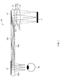
- FIG. 1 illustrates a configuration example of a virtual image display 10 according to an embodiment of the invention.
- the virtual image display 10 includes an image display element 11 as an image forming section displaying an image, and a virtual image optical system receiving display light displayed on the image display element 11 to guide the display light to a viewer's pupil 16.
- the image display element 11 is, for example, an organic EL display, an inorganic EL display, a liquid crystal display or the like.
- the image display element 11 displays an image through the use of light for N kinds (N is an integer of 1 or more) of wavelength bands. For example, in the case where color display is performed, an image is displayed through the use of light for a red wavelength band (red light), light for a green wavelength band (green light) and light for a blue wavelength band (blue light).
- the virtual image optical system includes a collimating optical system 12, a light guide plate 13, a first reflection type volume hologram grating 14 and a second reflection type volume hologram grating 15 both of which are arranged on the light guide plate 13.
- the collimating optical system 12 is an optical system receiving, for each of N kinds of wavelength bands, emitted from pixels of the image display element 11, and then converting the light beams into a plurality of parallel light beams with different view angles for each of the wavelength bands.
- the plurality of parallel light beams with different view angles enter the light guide plate 13.
- the parallel light beam L10 is a light beam with a central view angle which is emitted from a pixel in a central section of the image display element 11, and is converted into a light beam with a zero view angle (vertical to an incident surface of the light guide plate 13) by the collimating optical system 12 to enter the light guide plate 13.
- the parallel light beam L11 is a light beam with a peripheral view angle which is emitted from a pixel in a peripheral section of the image display element 11, and is converted into a light beam with a predetermined view angle (a predetermined view angle with respect to a normal to the surface of the light guide plate 13) by the collimating optical system 12 to enter the light guide plate 13.
- the parallel light beam L11 corresponds to a light beam with a view angle + ⁇ of illustrated in FIGs. 19 and 20 .
- the parallel light beam L12 is a light beam with another peripheral view angle which is emitted from a pixel in the another peripheral section of the image display element 11, and is converted into a light beam with another predetermined view angle (another predetermined view angle with respect to the normal to the surface of the light guide plate 13) by the collimating optical system 12 to enter the light guide plate 13.
- the parallel light beam L12 corresponds to a light beam with a view angle - ⁇ illustrated in FIGs. 19 and 20 .
- the light guide plate 13 receives, for each of the N kinds of wavelength bands, a plurality of parallel light beams with different traveling directions through the collimating optical system 12, and guides the received parallel light beams according to principle of total inner reflection.
- the light guide plate 13 is a light guide plate in the shape of a thin parallel plate including, as main surfaces, an optical surface 13a and an optical surface 13b facing the optical surface 13a.
- the optical surface 13a has a light inlet 13a1 at one end thereof to receive the parallel light beams with different view angles emitted from the collimating optical system 12.
- the optical surface 13a has a light outlet 13a2 at the other end thereof to emit light.
- the first reflection type volume hologram grating 14, hereinafter described as the first grating 14, is arranged in a position facing the light inlet 13a1 of the optical surface 13a
- the second reflection type volume hologram grating 15, hereinafter described as the second grating 15 is arranged in a position facing the light outlet 13a2 of the optical surface 13a.
- the first grating 14 diffracts and reflects the parallel light beams for each of the wavelength bands which have entered the light guide plate 13, so as to be reflected inside the light guide plate 13 according to the principle of total inner reflection.
- the second grating 15 diffracts and reflects the parallel light beams which have propagated inside the light guide plate 13 according to the principle of total inner reflection, so as to be emitted from the light guide plate 13 as they are in parallel.
- the first and second gratings 14 and 15 each have a diffraction configuration which includes N kinds of interference fringes each corresponding to the N kinds of the wavelength bands, and interference fringes each corresponding to the N kinds of the wavelength bands are recorded with uniform pitches p on a hologram surface.
- the first grating 14 is formed, for example, by laminating three layers, that is, hologram layers 14A, 14B and 14C.
- hologram layers 14A, 14B and 14C For example, interference fringes diffracting and reflecting mainly red light are recorded in the hologram layer 14A, and interference fringes diffracting and reflecting mainly blue light are recorded in the hologram layer 14B, and interference fringes diffracting and reflecting mainly green light are recorded in the hologram layer 14C.
- interference fringes with the same slant angle (slant of the interference fringes) ⁇ are recorded.
- the interference fringes in the hologram layer 14A, the interference fringes in the hologram layer 14B and the interference fringes in the hologram layer 14C are recorded with different pitches from one another.
- interference fringes in each of the hologram layers 14A, 14B and 14C are recorded with the same pitches irrespective of position. In other words, when the pitches between the interference fringes recorded in the hologram layer 14A is p, the interference fringes in the other hologram layers 14B and 14C are recorded with pitches different from the pitches p.
- the second grating 15 has a configuration symmetrical to that of the first grating 14. As illustrated in FIG. 3 , as in the case of the first grating 14, the second grating 15 is formed, for example, by laminating three layers, that is, hologram layers 15A, 15B and 15C. For example, interference fringes diffracting and reflecting mainly red light are recorded in the hologram layer 15A, and interference fringes diffracting and reflecting mainly blue light in the hologram layer 15B, and interference fringes diffracting and reflecting mainly green light are recorded in the hologram layer 15C. In each of the hologram layers 15A, 15B and 15C, for example, interference fringes with the same slant angle ⁇ are recorded.
- interference fringes in the hologram layer 15A, the interference fringes in the hologram layer 15B and the interference fringes in the hologram layer 15C are recorded with different pitches from one another. Moreover, interference fringes in each of the hologram layers 15A, 15B and 15C are recorded with the same pitches irrespective of position.
- the first and second gratings 14 and 15 have a configuration satisfying the following condition for each of the wavelength bands where a central diffraction wavelength defined as a diffraction wavelength at a central view angle (the reference view angle V) for each of the wavelength bands (for interference fringes of each color) is L, and the peak wavelength of the plurality of parallel light beams, for each of the wavelength bands, entering the light guide plate 13 is P.
- P>L Functions and effects by satisfying the condition will be described in detail later.
- FIGs. 4 and 5 illustrate diffraction configurations in other configuration examples different from the configurations illustrated in FIGs. 2 and 3 .
- interference fringes corresponding to N kinds of wavelength bands are multiplexed and recorded in the same layer.
- a first reflection type volume hologram grating 24, hereinafter described in the first grating 24, illustrated in FIG. 4 three kinds of interference fringes diffracting and reflecting red light, green light and blue light, that is, red light interference fringes 24R, green light interference fringes 24G, and blue light interference fringes 24B are multiplexed and recorded in the same layer.
- the three kinds of interference fringes are recorded so that grating pitches on a hologram surface 24S are uniform for each of the three kinds of interference fringes, but different between the three kinds of interference fringes.
- the pitch between the red light interference fringes 24R is p
- the green light interference fringes 24G and the blue light interference fringe 24B are formed with different pitches from the pitch p.
- the three kinds of interference fringes are recorded, for example, at the same slant angle ⁇ .
- a second reflection type volume hologram grating 25, hereinafter described the second grating 25, illustrated in FIG. 5 has a configuration symmetric to that of the first grating 24 illustrated in FIG. 4 .
- three kinds of interference fringes that is, red light interference fringes 25R, green light interference fringes 25G and blue light interference fringes 25B are multiplexed and recorded in the same layer.
- the three kinds of interference fringes are recorded so that grating pitches on a hologram surface 25S are uniform for each of the three kinds of interference fringes, but different between the three kinds of interference fringes.
- the pitch between the red light interference fringes 25R is p
- the green light interference fringes 25G and the blue light interference fringes 25B are formed with different pitches from the pitch p.
- the three kinds of interference fringes are recorded, for example, at the same slant angle ⁇ .
- the parallel light beams with different view angles entering from the light inlet 13a1 of the light guide plate 13 through the collimating optical system 12 enters the first grating 14, and each of the parallel light beams is diffracted and reflected as it is.
- the diffracted and reflected parallel light beams travel while being repeatedly totally reflected between the optical surface 13a and the optical surface 13b of the light guide plate 13 to enter the second grating 15.
- the light guide plate 13 is designed to have a sufficient length in a longitudinal direction and a thin thickness between the optical surface 13a and the optical surface 13b so as to have such an optical path length that the numbers of times of the total reflection of the parallel light beams with different view angles, while traveling inside the light guide plate 13 until the parallel light beams arrive at the second grating 15, depend on their view angles. More specifically, among the parallel light beams entering the light guide plate 13, the parallel light beam L11 entering at a view angle + ⁇ while being slanted toward the second grating 15, that is a parallel light beam with a large incident angle is reflected a smaller number of times than the parallel light beam L12 entering at a view angle - ⁇ which is in an opposite direction to the view angle + ⁇ .
- the parallel light beams with view angles entering the second grating 15 are diffracted and reflected thereby to deviate from conditions of total reflection, and then the parallel light beams are emitted from the light outlet 13a2 of the light guide plate 13 to enter a viewer's pupil 16.
- the second grating 15 and the first grating 14 are arranged on the optical surface 13b of the light guide plate 13 so that interference fringes recorded in the second grating 15 and interference fringes recorded in the first grating 14 are 180-degree rotationally symmetric to each other in a hologram plane. Therefore, the parallel light beams is reflected by the second grating 15 at an angle equal to an incident angle to the first grating 14, so a display image is displayed on the viewer's pupil 16 with high resolution without being blurred.
- the virtual image display 10 includes the first grating 14 and the second grating 15 which do not work as any lens, monochromatic eccentric aberration and diffraction chromatic aberration may be eliminated or reduced.
- the first grating 14 and the second grating 15 are arranged so that a hologram plane 14S of the first grating 14 and a hologram plane 15S of the second grating 15 are parallel to the optical surface 13b of the light guide plate 13.
- the invention is not limited thereto, and the hologram planes 14S and 15S may be arranged so as to have a predetermined angle with respect to the optical surface 13b.
- FIG. 6 illustrates a relationship between an incident or emission view angle and a central diffraction wavelength in the first or second grating 14 or 15. Examples of values illustrated in FIG. 6 are values under the following specifications. In addition, in the values illustrated in FIG. 6 , the view angle ⁇ of a minus value corresponds to a view angle - ⁇ illustrated in FIGs. 19 and 20 in the case where the second grating 15 is used as an example.
- Wavelength band ⁇ (peak wavelength) of light beam entering light guide plate 635 nm
- Refractive index n of light guide plate 1.52
- the central diffraction wavelength of the first or second reflection type volume hologram gratins 14 or 15 under the above-described specifications are continuously shifted by the view angle as illustrated in FIG. 6 , because Bragg conditions are changed depending on the incident angle of the parallel light beam.
- the view angle of a parallel light beam which is totally reflected inside the second grating 15 a larger number of times causes an increase in the number of times the light beam is diffracted and reflected by the second grating 15, thereby an image is dark when a viewer observes the image.
- the intensity of the light beam diffracted and reflected for the first time to be emitted is 30%
- the intensity of the emitted light beam diffracted and reflected for the second time is 21% because 30% of the intensity (70%) of the light beam not diffracted and reflected for the first time is diffracted, and in the same manner, the intensity of the light beam diffracted and reflected for the third time to be emitted is 14.7%
- the intensity of the light beam diffracted and reflected for the fourth time to be emitted is 10.29%.
- the intensity of a light beam with a view angle which is viewable by being diffracted and reflected for the fourth time is about 1/3 of the intensity of a light beam with a view angle which is viewable by being diffracted and reflected for the first time.
- Such a decline in light intensity occurs even in the case where the diffraction efficiency of the second grating 15 is changed.
- FIG. 7 illustrates a relationship between the number of times light is internally diffracted and reflected and the intensity of emitted light in the second grating 15 in the case where the diffraction efficiency is changed.
- the spectrum distribution of light with each view angle which is diffracted and reflected from the second grating 15 is represented by the product of the diffraction efficiency distributions of the first and second gratings 14 and 15 in which the central diffraction wavelength is shifted by the spectrum distribution of the LED and Bragg conditions.
- the peak wavelength of the LED is brought near the central diffraction wavelength of a light beam with a view angle which is diffracted and reflected a large number of times, for example, 3 or 4 times thereby to compensate for a decline in light intensity of the light beam with a view angle which is diffracted and reflected a large number of times and to increase the intensity of the light beam with the view angle. Therefore, the light intensity balance between light beams with different view angles is struck.
- FIG. 10 illustrates the configuration of the virtual image display 10 in the example.
- the virtual image display 10 was formed so that the thickness of the first grating 14 was 7 ⁇ m, and the thickness of the second grating 15 was 5 ⁇ m, and the surface pitches p of the first and second gratings 14 and 15 was 0.531 ⁇ m, and the slant angle ⁇ of the interference fringe was 64.5 degrees, and ⁇ n was 0.05.
- " ⁇ n" represents a modulated width of the refractive index of each of the first and second gratings 14 and 15 diffracting and reflecting light beams by the periodical modulation of the refractive index in a medium.
- the first and second gratings 14 and 15 were arranged on the light guide plate 13 with a thickness of 1 mm so as to have a space of 30 mm therebetween, and the parallel light beams emitted from the image display element 11 and collimated at a view angle of ⁇ 8 degrees by the collimating optical system 12 was allowed to enter the first grating 14, and a virtual image was observed by the CCD camera 17 at the viewer's pupil position O.
- the wavelength band diffracted and reflected by the first and second gratings 14 and 15 in the example was 585 nm to 670 nm in a range of the view angle (i.e., incident angle) of t8 degrees as illustrated in FIGs. 11 and 12 , and the central wavelength was substantially equal to a diffraction wavelength of 630 nm at the central view angle of 0 degrees.
- FIG. 11 illustrates the diffraction reflection spectrum of the first grating 14
- FIG. 12 illustrates the diffraction reflection spectrum of the second grating 15.
- FIG. 13 illustrates the spectrum distribution of a light source (the red LED) illuminating the image display element 11 used in the example.
- the diffraction efficiency distributions at each view angle of the first and second gratings 14 and 15 are as illustrated in FIGs. 11 and 12 , and in the case where a light source illustrated in FIG. 13 is used, the LED spectrums of light beams, diffracted and reflected by the second grating 15, at the view angle of ⁇ 8 degrees and the central view angle are as illustrated in FIG. 14 .
- FIG. 15 A result obtained by measuring a light intensity distribution in a horizontal direction of a virtual image plane observed in the viewer's pupil position O in the example by the CCD camera 17 is illustrated in FIG. 15 .
- the peak wavelength of the red LED at this time was 645 nm, and the peak wavelength compensated for a decline in the intensity of a light beam with a view angle of +8 degrees by diffracting and reflecting the light beam a plurality of times.
- the relationship P>L is satisfied by changing the spectrum distribution of the light source of the image display element 11 is described.
- the relationship P>L may be satisfied by changing the diffraction configurations of the first and second gratings 14 and 15.
- the central diffraction wavelength L in the first and second gratings 14 and 15 and the peak wavelength P of the parallel light beams entering the light guide plate 13 satisfy a predetermined relationship so as to compensate for a decline in intensity of the light beam with a view angle which is diffracted and reflected a large number of times in the second grating 15, so the light intensity balance between light beams with different view angles is favorably maintained, and virtual images with less unevenness in brightness may be observed.
- the present invention is not limited to the above-described embodiment, and may be variously modified.
- first and second gratings 84a and 84c in the virtual image display 80 are configured so that a central diffraction wavelength L at a central view angle satisfies the following relationship with a peak wavelength P of parallel light beams which is to enter a light guide plate 83.
- the present invention is applicable to apparatuses displaying an enlarged virtual image in substantially the same principle as that in the virtual image display illustrated in FIG. 1 or FIG. 18 through the use of a reflection type volume hologram grating.
Landscapes
- Physics & Mathematics (AREA)
- General Physics & Mathematics (AREA)
- Optics & Photonics (AREA)
- Engineering & Computer Science (AREA)
- Microelectronics & Electronic Packaging (AREA)
- Diffracting Gratings Or Hologram Optical Elements (AREA)
Applications Claiming Priority (1)
| Application Number | Priority Date | Filing Date | Title |
|---|---|---|---|
| JP2008151430A JP4518193B2 (ja) | 2008-06-10 | 2008-06-10 | 光学装置および虚像表示装置 |
Publications (2)
| Publication Number | Publication Date |
|---|---|
| EP2133727A1 true EP2133727A1 (de) | 2009-12-16 |
| EP2133727B1 EP2133727B1 (de) | 2013-03-13 |
Family
ID=40999875
Family Applications (1)
| Application Number | Title | Priority Date | Filing Date |
|---|---|---|---|
| EP09006129A Not-in-force EP2133727B1 (de) | 2008-06-10 | 2009-05-05 | Optische Vorrichtung und virtuelle Bildanzeige |
Country Status (3)
| Country | Link |
|---|---|
| US (4) | US8325166B2 (de) |
| EP (1) | EP2133727B1 (de) |
| JP (1) | JP4518193B2 (de) |
Cited By (6)
| Publication number | Priority date | Publication date | Assignee | Title |
|---|---|---|---|---|
| WO2011089433A1 (en) * | 2010-01-25 | 2011-07-28 | Bae Systems Plc | Projection display |
| EP2360509A1 (de) * | 2010-01-25 | 2011-08-24 | BAE Systems PLC | Projektionsanzeige |
| WO2014140620A3 (en) * | 2013-03-14 | 2014-11-27 | The Secretary Of State For Business, Innovation & Skills | Display and method of operating a display |
| EP3301501A1 (de) * | 2016-09-30 | 2018-04-04 | Nokia Technologies OY | Vorrichtung für erweiterte realität |
| WO2019213158A1 (en) * | 2018-05-01 | 2019-11-07 | Facebook Technologies, Llc | 2d pupil expander using holographic bragg grating |
| EP3553586B1 (de) * | 2007-11-29 | 2023-02-15 | Sony Group Corporation | Bildanzeigevorrichtung |
Families Citing this family (127)
| Publication number | Priority date | Publication date | Assignee | Title |
|---|---|---|---|---|
| GB0522968D0 (en) | 2005-11-11 | 2005-12-21 | Popovich Milan M | Holographic illumination device |
| GB0718706D0 (en) | 2007-09-25 | 2007-11-07 | Creative Physics Ltd | Method and apparatus for reducing laser speckle |
| US11726332B2 (en) | 2009-04-27 | 2023-08-15 | Digilens Inc. | Diffractive projection apparatus |
| US9335604B2 (en) | 2013-12-11 | 2016-05-10 | Milan Momcilo Popovich | Holographic waveguide display |
| US11204540B2 (en) | 2009-10-09 | 2021-12-21 | Digilens Inc. | Diffractive waveguide providing a retinal image |
| WO2011042711A2 (en) | 2009-10-09 | 2011-04-14 | Milan Momcilo Popovich | Compact edge illuminated diffractive display |
| EP2431786A1 (de) * | 2010-09-17 | 2012-03-21 | Bayer MaterialScience AG | Autostereoskopisches 3D-Display |
| JP5703880B2 (ja) * | 2011-03-22 | 2015-04-22 | セイコーエプソン株式会社 | 導光板及びこれを備える虚像表示装置 |
| WO2012136970A1 (en) | 2011-04-07 | 2012-10-11 | Milan Momcilo Popovich | Laser despeckler based on angular diversity |
| WO2016020630A2 (en) | 2014-08-08 | 2016-02-11 | Milan Momcilo Popovich | Waveguide laser illuminator incorporating a despeckler |
| US10670876B2 (en) | 2011-08-24 | 2020-06-02 | Digilens Inc. | Waveguide laser illuminator incorporating a despeckler |
| EP2748670B1 (de) | 2011-08-24 | 2015-11-18 | Rockwell Collins, Inc. | Tragbare datenanzeige |
| JP5929136B2 (ja) | 2011-12-05 | 2016-06-01 | セイコーエプソン株式会社 | 電気光学装置および電子機器 |
| WO2013102759A2 (en) | 2012-01-06 | 2013-07-11 | Milan Momcilo Popovich | Contact image sensor using switchable bragg gratings |
| JP2013200467A (ja) * | 2012-03-26 | 2013-10-03 | Seiko Epson Corp | 虚像表示装置 |
| CN103562802B (zh) | 2012-04-25 | 2016-08-17 | 罗克韦尔柯林斯公司 | 全息广角显示器 |
| US9456744B2 (en) | 2012-05-11 | 2016-10-04 | Digilens, Inc. | Apparatus for eye tracking |
| US8913324B2 (en) * | 2012-08-07 | 2014-12-16 | Nokia Corporation | Display illumination light guide |
| US8724206B2 (en) * | 2012-09-28 | 2014-05-13 | Google Inc. | Photo-chromic coating for optics |
| US9933684B2 (en) * | 2012-11-16 | 2018-04-03 | Rockwell Collins, Inc. | Transparent waveguide display providing upper and lower fields of view having a specific light output aperture configuration |
| KR102046104B1 (ko) * | 2013-03-19 | 2019-11-18 | 삼성전자주식회사 | 홀로그래픽 3차원 영상 디스플레이 장치 및 상기 홀로그래픽 3차원 영상 디스플레이 장치용 조광 유닛 |
| WO2014188149A1 (en) | 2013-05-20 | 2014-11-27 | Milan Momcilo Popovich | Holographic waveguide eye tracker |
| CN103353667B (zh) | 2013-06-28 | 2015-10-21 | 北京智谷睿拓技术服务有限公司 | 成像调整设备及方法 |
| CN103353663B (zh) | 2013-06-28 | 2016-08-10 | 北京智谷睿拓技术服务有限公司 | 成像调整装置及方法 |
| CN103353677B (zh) | 2013-06-28 | 2015-03-11 | 北京智谷睿拓技术服务有限公司 | 成像装置及方法 |
| WO2015015138A1 (en) | 2013-07-31 | 2015-02-05 | Milan Momcilo Popovich | Method and apparatus for contact image sensing |
| CN103424891B (zh) | 2013-07-31 | 2014-12-17 | 北京智谷睿拓技术服务有限公司 | 成像装置及方法 |
| CN103431840B (zh) | 2013-07-31 | 2016-01-20 | 北京智谷睿拓技术服务有限公司 | 眼睛光学参数检测系统及方法 |
| CN103431980A (zh) | 2013-08-22 | 2013-12-11 | 北京智谷睿拓技术服务有限公司 | 视力保护成像系统及方法 |
| CN103439801B (zh) | 2013-08-22 | 2016-10-26 | 北京智谷睿拓技术服务有限公司 | 视力保护成像装置及方法 |
| CN103605208B (zh) * | 2013-08-30 | 2016-09-28 | 北京智谷睿拓技术服务有限公司 | 内容投射系统及方法 |
| CN103500331B (zh) | 2013-08-30 | 2017-11-10 | 北京智谷睿拓技术服务有限公司 | 提醒方法及装置 |
| TWI518368B (zh) * | 2013-09-11 | 2016-01-21 | 財團法人工業技術研究院 | 虛像顯示裝置 |
| US10194860B2 (en) | 2013-09-11 | 2019-02-05 | Industrial Technology Research Institute | Virtual image display system |
| CN103558909B (zh) | 2013-10-10 | 2017-03-29 | 北京智谷睿拓技术服务有限公司 | 交互投射显示方法及交互投射显示系统 |
| RU2594370C2 (ru) | 2014-07-11 | 2016-08-20 | Самсунг Электроникс Ко., Лтд. | Световодная структура, оптическое устройство и система формирования изображений |
| RU2603238C2 (ru) | 2014-07-15 | 2016-11-27 | Самсунг Электроникс Ко., Лтд. | Световодная структура, голографическое оптическое устройство и система формирования изображений |
| WO2016020632A1 (en) | 2014-08-08 | 2016-02-11 | Milan Momcilo Popovich | Method for holographic mastering and replication |
| CN104199196B (zh) * | 2014-09-04 | 2017-02-15 | 北京理工大学 | 一种具有眼动追踪功能的波导式集成成像三维显示系统 |
| US10241330B2 (en) | 2014-09-19 | 2019-03-26 | Digilens, Inc. | Method and apparatus for generating input images for holographic waveguide displays |
| WO2016046514A1 (en) | 2014-09-26 | 2016-03-31 | LOKOVIC, Kimberly, Sun | Holographic waveguide opticaltracker |
| JP6507567B2 (ja) * | 2014-10-29 | 2019-05-08 | セイコーエプソン株式会社 | 光学素子および画像表示装置 |
| JP5974375B2 (ja) * | 2014-12-01 | 2016-08-23 | セイコーエプソン株式会社 | 虚像表示装置 |
| CN104570353A (zh) * | 2015-01-08 | 2015-04-29 | 浙江大学 | 利用全息波导进行彩色目视显示的方法、光学系统及穿戴设备 |
| EP3245551B1 (de) | 2015-01-12 | 2019-09-18 | DigiLens Inc. | Lichtfeldanzeigen mit wellenleiter |
| WO2016113534A1 (en) | 2015-01-12 | 2016-07-21 | Milan Momcilo Popovich | Environmentally isolated waveguide display |
| WO2016116733A1 (en) | 2015-01-20 | 2016-07-28 | Milan Momcilo Popovich | Holographic waveguide lidar |
| US9541998B2 (en) * | 2015-01-29 | 2017-01-10 | Samsung Electronics Co., Ltd. | Electronic system with gaze alignment mechanism and method of operation thereof |
| US9632226B2 (en) | 2015-02-12 | 2017-04-25 | Digilens Inc. | Waveguide grating device |
| US10459145B2 (en) | 2015-03-16 | 2019-10-29 | Digilens Inc. | Waveguide device incorporating a light pipe |
| US10591756B2 (en) | 2015-03-31 | 2020-03-17 | Digilens Inc. | Method and apparatus for contact image sensing |
| US11988854B2 (en) | 2015-08-24 | 2024-05-21 | Akonia Holographics Llc | Wide field-of-view holographic skew mirrors |
| US10180520B2 (en) | 2015-08-24 | 2019-01-15 | Akonia Holographics, Llc | Skew mirrors, methods of use, and methods of manufacture |
| CN113759555B (zh) | 2015-10-05 | 2024-09-20 | 迪吉伦斯公司 | 波导显示器 |
| KR102367308B1 (ko) * | 2016-01-30 | 2022-02-24 | 레이아 인코포레이티드 | 수렴 시점들을 갖는 다중 빔 요소-기반 역광 조명 |
| US10983340B2 (en) | 2016-02-04 | 2021-04-20 | Digilens Inc. | Holographic waveguide optical tracker |
| IL244181B (en) * | 2016-02-18 | 2020-06-30 | Amitai Yaakov | Compact head-up display system |
| KR102526753B1 (ko) * | 2016-02-26 | 2023-04-27 | 삼성전자주식회사 | 가간섭성 백라이트 유닛, 및 이를 채용한 3차원 영상 표시 장치 |
| CN108780224B (zh) | 2016-03-24 | 2021-08-03 | 迪吉伦斯公司 | 用于提供偏振选择性全息波导装置的方法和设备 |
| US10815145B2 (en) | 2016-03-31 | 2020-10-27 | Corning Incorporated | High index glass and devices incorporating such |
| JP7001613B2 (ja) * | 2016-04-06 | 2022-01-19 | アコニア ホログラフィックス、エルエルシー | 広視野のホログラフィックスキューミラー |
| JP6734933B2 (ja) | 2016-04-11 | 2020-08-05 | ディジレンズ インコーポレイテッド | 構造化光投影のためのホログラフィック導波管装置 |
| JP6264405B2 (ja) * | 2016-07-13 | 2018-01-24 | セイコーエプソン株式会社 | 虚像表示装置 |
| US10663756B2 (en) | 2016-07-18 | 2020-05-26 | Lumens Co., Ltd. | Display apparatus |
| KR102527099B1 (ko) | 2016-07-18 | 2023-05-02 | 주식회사 루멘스 | 디스플레이 장치 |
| KR102509703B1 (ko) | 2016-07-18 | 2023-03-15 | 주식회사 루멘스 | 도파관을 이용하는 3d 디스플레이 장치 |
| CN110073252B (zh) * | 2016-10-12 | 2021-12-24 | 阿科尼亚全息有限责任公司 | 空间变化的倾斜镜 |
| KR102822335B1 (ko) * | 2016-11-11 | 2025-06-18 | 삼성전자주식회사 | 백라이트 유닛, 이를 포함한 홀로그래픽 디스플레이 및 홀로그래픽 광학 소자의 제조 방법 |
| JP2018084725A (ja) * | 2016-11-25 | 2018-05-31 | セイコーエプソン株式会社 | 表示装置 |
| US11513350B2 (en) | 2016-12-02 | 2022-11-29 | Digilens Inc. | Waveguide device with uniform output illumination |
| WO2018106253A1 (en) | 2016-12-09 | 2018-06-14 | University Of Central Florida Research Foundation, Inc. | Optical display system, method, and applications |
| WO2018129398A1 (en) | 2017-01-05 | 2018-07-12 | Digilens, Inc. | Wearable heads up displays |
| CN115166977B (zh) | 2017-02-13 | 2025-04-25 | 视瑞尔技术公司 | 光导装置和用于表示场景的显示装置 |
| CN110462487B (zh) | 2017-03-21 | 2022-07-01 | 奇跃公司 | 用于组合视场的具有不同衍射光栅的堆叠波导 |
| JP6852501B2 (ja) * | 2017-03-28 | 2021-03-31 | セイコーエプソン株式会社 | 表示装置 |
| RU180402U1 (ru) * | 2017-04-17 | 2018-06-13 | Общество С Ограниченной Ответственностью "Изовак Технологии" | Оптическое устройство для формирования изображений дополненной реальности |
| CN108474951B (zh) * | 2017-05-02 | 2020-12-25 | 深圳市柔宇科技股份有限公司 | 全息波导显示系统 |
| CN110678802B (zh) * | 2017-05-16 | 2021-12-03 | 奇跃公司 | 用于混合现实的系统和方法 |
| JP2019020723A (ja) * | 2017-07-12 | 2019-02-07 | Hoya Candeo Optronics株式会社 | 導光板、画像表示装置 |
| KR102642282B1 (ko) * | 2017-07-12 | 2024-02-28 | 호야 가부시키가이샤 | 도광판 및 화상 표시 장치 |
| US10859833B2 (en) * | 2017-08-18 | 2020-12-08 | Tipd, Llc | Waveguide image combiner for augmented reality displays |
| US11668935B2 (en) | 2017-08-18 | 2023-06-06 | A9.Com, Inc. | Waveguide image combiners for augmented reality displays |
| US11789265B2 (en) | 2017-08-18 | 2023-10-17 | A9.Com, Inc. | Waveguide image combiners for augmented reality displays |
| US11698492B2 (en) * | 2017-08-18 | 2023-07-11 | A9.Com, Inc. | Waveguide image combiners for augmented reality displays |
| US11841481B2 (en) * | 2017-09-21 | 2023-12-12 | Magic Leap, Inc. | Augmented reality display with waveguide configured to capture images of eye and/or environment |
| EP3698214A4 (de) | 2017-10-16 | 2021-10-27 | Digilens Inc. | Systeme und verfahren zum multiplizieren der bildauflösung einer pixelierten anzeige |
| JP6436221B2 (ja) * | 2017-12-18 | 2018-12-12 | セイコーエプソン株式会社 | 虚像表示装置 |
| DE102017130344A1 (de) * | 2017-12-18 | 2019-06-19 | Carl Zeiss Ag | Optisches System zum Übertragen eines Quellbildes |
| CN107966819A (zh) * | 2017-12-27 | 2018-04-27 | 北京灵犀微光科技有限公司 | 波导显示装置 |
| CN111566571B (zh) | 2018-01-08 | 2022-05-13 | 迪吉伦斯公司 | 波导单元格中全息光栅高吞吐量记录的系统和方法 |
| CN114721242B (zh) | 2018-01-08 | 2025-08-15 | 迪吉伦斯公司 | 用于制造光学波导的方法 |
| US10914950B2 (en) | 2018-01-08 | 2021-02-09 | Digilens Inc. | Waveguide architectures and related methods of manufacturing |
| WO2019135837A1 (en) | 2018-01-08 | 2019-07-11 | Digilens, Inc. | Systems and methods for manufacturing waveguide cells |
| EP4372451A3 (de) | 2018-03-16 | 2024-08-14 | Digilens Inc. | Holographische wellenleiter mit doppelbrechungssteuerung und verfahren zu ihrer herstellung |
| CN110297331A (zh) | 2018-03-23 | 2019-10-01 | 京东方科技集团股份有限公司 | 显示装置及显示方法 |
| US10877214B2 (en) | 2018-05-04 | 2020-12-29 | Facebook Technologies, Llc | Diffraction gratings for beam redirection |
| US11402801B2 (en) | 2018-07-25 | 2022-08-02 | Digilens Inc. | Systems and methods for fabricating a multilayer optical structure |
| JP7376578B2 (ja) | 2018-09-26 | 2023-11-08 | マジック リープ, インコーポレイテッド | ピンホールおよびスリットカメラを伴うアイウェア |
| WO2020149956A1 (en) | 2019-01-14 | 2020-07-23 | Digilens Inc. | Holographic waveguide display with light control layer |
| DE102019102605A1 (de) * | 2019-02-01 | 2020-08-06 | Carl Zeiss Jena Gmbh | Funktionalisierter Wellenleiter für ein Detektorsystem |
| US20200247017A1 (en) | 2019-02-05 | 2020-08-06 | Digilens Inc. | Methods for Compensating for Optical Surface Nonuniformity |
| KR102866596B1 (ko) | 2019-02-15 | 2025-09-29 | 디지렌즈 인코포레이티드. | 일체형 격자를 이용하여 홀로그래픽 도파관 디스플레이를 제공하기 위한 방법 및 장치 |
| US20220283377A1 (en) | 2019-02-15 | 2022-09-08 | Digilens Inc. | Wide Angle Waveguide Display |
| US11372246B2 (en) * | 2019-02-22 | 2022-06-28 | Facebook Technologies, Llc | Near-eye display system having optical combiner |
| WO2020186113A1 (en) | 2019-03-12 | 2020-09-17 | Digilens Inc. | Holographic waveguide backlight and related methods of manufacturing |
| JP7275829B2 (ja) * | 2019-05-13 | 2023-05-18 | セイコーエプソン株式会社 | 表示装置および画像の表示方法 |
| KR20220016990A (ko) | 2019-06-07 | 2022-02-10 | 디지렌즈 인코포레이티드. | 투과 및 반사 격자를 통합하는 도파관 및 관련 제조 방법 |
| US11681143B2 (en) | 2019-07-29 | 2023-06-20 | Digilens Inc. | Methods and apparatus for multiplying the image resolution and field-of-view of a pixelated display |
| TWI762947B (zh) * | 2019-08-22 | 2022-05-01 | 宏達國際電子股份有限公司 | 顯示裝置 |
| WO2021041949A1 (en) | 2019-08-29 | 2021-03-04 | Digilens Inc. | Evacuating bragg gratings and methods of manufacturing |
| DE102019212988A1 (de) * | 2019-08-29 | 2021-03-04 | Audi Ag | Kameravorrichtung zum Erzeugen eines Abbilds einer Umgebung |
| CN112444968B (zh) * | 2019-08-29 | 2022-04-22 | 华为技术有限公司 | 一种增强现实的光学叠加器和相关设备 |
| US11467331B1 (en) | 2019-10-29 | 2022-10-11 | Meta Platforms Technologies, Llc | Optical combiner with uniform illuminance throughput |
| JP7494483B2 (ja) * | 2020-02-21 | 2024-06-04 | 大日本印刷株式会社 | 光学部材、表示装置、頭部装着型表示装置 |
| CN113703174B (zh) * | 2020-05-22 | 2024-08-06 | 富泰华工业(深圳)有限公司 | 全息显示装置 |
| FI130494B (en) * | 2020-05-29 | 2023-10-06 | Dispelix Oy | Improved output pupil dilator |
| CN113900264B (zh) * | 2020-06-22 | 2024-08-13 | 富泰华工业(深圳)有限公司 | 全息显示装置 |
| JP7466903B2 (ja) * | 2020-09-23 | 2024-04-15 | 国立研究開発法人情報通信研究機構 | Ar表示装置用光学素子及びその製造方法、並びに、ar表示装置 |
| EP4224239B1 (de) * | 2020-11-30 | 2025-07-16 | Nokia Technologies Oy | Optische vorrichtung, module und vorrichtungen |
| US11947314B2 (en) | 2020-12-15 | 2024-04-02 | A9.Com, Inc. | Volume holographic optical elements with expanded angular acceptance |
| KR20230119015A (ko) | 2020-12-21 | 2023-08-14 | 디지렌즈 인코포레이티드. | 도파로 기반 디스플레이에서의 홍목현상 억제 기술 |
| US12399326B2 (en) | 2021-01-07 | 2025-08-26 | Digilens Inc. | Grating structures for color waveguides |
| KR20230153459A (ko) | 2021-03-05 | 2023-11-06 | 디지렌즈 인코포레이티드. | 진공 주기적 구조체 및 제조 방법 |
| CN115128737B (zh) * | 2021-03-24 | 2023-04-18 | 华为技术有限公司 | 衍射光波导及电子设备 |
| US12259686B2 (en) | 2021-05-21 | 2025-03-25 | Amazon Technologies, Inc. | Waveguide geometry for improved display performance |
| KR102627824B1 (ko) * | 2021-08-11 | 2024-01-23 | 주식회사 레티널 | 회절 소자를 이용한 증강 현실용 광학 장치 |
| KR102627825B1 (ko) * | 2021-08-30 | 2024-01-23 | 주식회사 레티널 | 회절 소자를 이용한 컴팩트형 증강 현실용 광학 장치 |
Citations (4)
| Publication number | Priority date | Publication date | Assignee | Title |
|---|---|---|---|---|
| EP1536268A1 (de) * | 2002-07-26 | 2005-06-01 | Nikon Corporation | Bildkombinierer und bildanzeigeeinheit |
| WO2005093493A1 (ja) | 2004-03-29 | 2005-10-06 | Sony Corporation | 光学装置及び虚像表示装置 |
| EP1619536A1 (de) * | 2003-04-28 | 2006-01-25 | Nikon Corporation | Bildkombinierer und bildanzeige |
| US20060291021A1 (en) * | 2005-06-17 | 2006-12-28 | Hiroshi Mukawa | Optical device, and virtual image display |
Family Cites Families (7)
| Publication number | Priority date | Publication date | Assignee | Title |
|---|---|---|---|---|
| US4711512A (en) * | 1985-07-12 | 1987-12-08 | Environmental Research Institute Of Michigan | Compact head-up display |
| JP2005093493A (ja) | 2003-09-12 | 2005-04-07 | Tamura Seisakusho Co Ltd | 低背型トランスの製造方法および低背型トランス |
| JP4810949B2 (ja) * | 2005-09-29 | 2011-11-09 | ソニー株式会社 | 光学装置及び画像表示装置 |
| JP4872499B2 (ja) * | 2006-07-14 | 2012-02-08 | ソニー株式会社 | 回折格子部材、光学装置、及び、画像表示装置 |
| JP4779887B2 (ja) * | 2006-09-01 | 2011-09-28 | ソニー株式会社 | 画像表示装置 |
| JP2008058777A (ja) * | 2006-09-01 | 2008-03-13 | Sony Corp | 光学装置及び画像表示装置 |
| JP4450058B2 (ja) * | 2007-11-29 | 2010-04-14 | ソニー株式会社 | 画像表示装置 |
-
2008
- 2008-06-10 JP JP2008151430A patent/JP4518193B2/ja not_active Expired - Fee Related
-
2009
- 2009-05-05 EP EP09006129A patent/EP2133727B1/de not_active Not-in-force
- 2009-06-09 US US12/481,284 patent/US8325166B2/en not_active Expired - Fee Related
-
2012
- 2012-11-15 US US13/677,588 patent/US8810878B2/en active Active
-
2014
- 2014-06-17 US US14/306,595 patent/US9383722B2/en active Active
-
2016
- 2016-06-23 US US15/190,532 patent/US10025100B2/en active Active
Patent Citations (4)
| Publication number | Priority date | Publication date | Assignee | Title |
|---|---|---|---|---|
| EP1536268A1 (de) * | 2002-07-26 | 2005-06-01 | Nikon Corporation | Bildkombinierer und bildanzeigeeinheit |
| EP1619536A1 (de) * | 2003-04-28 | 2006-01-25 | Nikon Corporation | Bildkombinierer und bildanzeige |
| WO2005093493A1 (ja) | 2004-03-29 | 2005-10-06 | Sony Corporation | 光学装置及び虚像表示装置 |
| US20060291021A1 (en) * | 2005-06-17 | 2006-12-28 | Hiroshi Mukawa | Optical device, and virtual image display |
Cited By (9)
| Publication number | Priority date | Publication date | Assignee | Title |
|---|---|---|---|---|
| EP3553586B1 (de) * | 2007-11-29 | 2023-02-15 | Sony Group Corporation | Bildanzeigevorrichtung |
| WO2011089433A1 (en) * | 2010-01-25 | 2011-07-28 | Bae Systems Plc | Projection display |
| EP2360509A1 (de) * | 2010-01-25 | 2011-08-24 | BAE Systems PLC | Projektionsanzeige |
| US8810913B2 (en) | 2010-01-25 | 2014-08-19 | Bae Systems Plc | Projection display |
| WO2014140620A3 (en) * | 2013-03-14 | 2014-11-27 | The Secretary Of State For Business, Innovation & Skills | Display and method of operating a display |
| EP3301501A1 (de) * | 2016-09-30 | 2018-04-04 | Nokia Technologies OY | Vorrichtung für erweiterte realität |
| WO2018060557A1 (en) * | 2016-09-30 | 2018-04-05 | Nokia Technologies Oy | Augmented reality apparatus |
| US11054652B2 (en) | 2016-09-30 | 2021-07-06 | Nokia Technologies Oy | Augmented reality apparatus |
| WO2019213158A1 (en) * | 2018-05-01 | 2019-11-07 | Facebook Technologies, Llc | 2d pupil expander using holographic bragg grating |
Also Published As
| Publication number | Publication date |
|---|---|
| US9383722B2 (en) | 2016-07-05 |
| US20180011321A1 (en) | 2018-01-11 |
| US8810878B2 (en) | 2014-08-19 |
| US20130077141A1 (en) | 2013-03-28 |
| US20090303212A1 (en) | 2009-12-10 |
| JP2009300480A (ja) | 2009-12-24 |
| US20140293389A1 (en) | 2014-10-02 |
| EP2133727B1 (de) | 2013-03-13 |
| US8325166B2 (en) | 2012-12-04 |
| US10025100B2 (en) | 2018-07-17 |
| JP4518193B2 (ja) | 2010-08-04 |
Similar Documents
| Publication | Publication Date | Title |
|---|---|---|
| EP2133727B1 (de) | Optische Vorrichtung und virtuelle Bildanzeige | |
| EP2065751B1 (de) | Bildanzeigevorrichtung | |
| US7453612B2 (en) | Optical device, and virtual image display | |
| US7499216B2 (en) | Wide field-of-view binocular device | |
| US10180574B2 (en) | Image display apparatus | |
| US20240027670A1 (en) | Photonic Crystals and Methods for Fabricating the Same | |
| US7502168B2 (en) | Optical device and image display apparatus | |
| JP2010044172A (ja) | 虚像表示装置 | |
| US20110242661A1 (en) | waveguides | |
| IL299401A (en) | Stacked waveguides with different refractive gratings for an integrated field of view | |
| JP2010271565A (ja) | 頭部装着型表示装置 | |
| US10805582B2 (en) | Method and device for generating and decoding spectrally encoded images | |
| US10579015B2 (en) | Reflective holographic display apparatus and display method for the same | |
| JP2015102613A (ja) | 光学デバイス、及び、表示装置 | |
| EP4675333A1 (de) | Farbholographische optische wellenleiter-anzeigevorrichtung mit einer einzigen schicht | |
| JP2021092749A (ja) | 光学部材及び表示装置 | |
| US20110228395A1 (en) | Apparatus for illuminating a reticle | |
| US20240192423A1 (en) | Image display device and image display method |
Legal Events
| Date | Code | Title | Description |
|---|---|---|---|
| PUAI | Public reference made under article 153(3) epc to a published international application that has entered the european phase |
Free format text: ORIGINAL CODE: 0009012 |
|
| 17P | Request for examination filed |
Effective date: 20090505 |
|
| AK | Designated contracting states |
Kind code of ref document: A1 Designated state(s): AT BE BG CH CY CZ DE DK EE ES FI FR GB GR HR HU IE IS IT LI LT LU LV MC MK MT NL NO PL PT RO SE SI SK TR |
|
| GRAP | Despatch of communication of intention to grant a patent |
Free format text: ORIGINAL CODE: EPIDOSNIGR1 |
|
| GRAS | Grant fee paid |
Free format text: ORIGINAL CODE: EPIDOSNIGR3 |
|
| GRAA | (expected) grant |
Free format text: ORIGINAL CODE: 0009210 |
|
| AK | Designated contracting states |
Kind code of ref document: B1 Designated state(s): AT BE BG CH CY CZ DE DK EE ES FI FR GB GR HR HU IE IS IT LI LT LU LV MC MK MT NL NO PL PT RO SE SI SK TR |
|
| REG | Reference to a national code |
Ref country code: GB Ref legal event code: FG4D |
|
| REG | Reference to a national code |
Ref country code: CH Ref legal event code: EP Ref country code: AT Ref legal event code: REF Ref document number: 601131 Country of ref document: AT Kind code of ref document: T Effective date: 20130315 |
|
| REG | Reference to a national code |
Ref country code: IE Ref legal event code: FG4D |
|
| REG | Reference to a national code |
Ref country code: DE Ref legal event code: R096 Ref document number: 602009013816 Country of ref document: DE Effective date: 20130508 |
|
| PG25 | Lapsed in a contracting state [announced via postgrant information from national office to epo] |
Ref country code: LT Free format text: LAPSE BECAUSE OF FAILURE TO SUBMIT A TRANSLATION OF THE DESCRIPTION OR TO PAY THE FEE WITHIN THE PRESCRIBED TIME-LIMIT Effective date: 20130313 Ref country code: SE Free format text: LAPSE BECAUSE OF FAILURE TO SUBMIT A TRANSLATION OF THE DESCRIPTION OR TO PAY THE FEE WITHIN THE PRESCRIBED TIME-LIMIT Effective date: 20130313 Ref country code: ES Free format text: LAPSE BECAUSE OF FAILURE TO SUBMIT A TRANSLATION OF THE DESCRIPTION OR TO PAY THE FEE WITHIN THE PRESCRIBED TIME-LIMIT Effective date: 20130624 Ref country code: NO Free format text: LAPSE BECAUSE OF FAILURE TO SUBMIT A TRANSLATION OF THE DESCRIPTION OR TO PAY THE FEE WITHIN THE PRESCRIBED TIME-LIMIT Effective date: 20130613 Ref country code: BG Free format text: LAPSE BECAUSE OF FAILURE TO SUBMIT A TRANSLATION OF THE DESCRIPTION OR TO PAY THE FEE WITHIN THE PRESCRIBED TIME-LIMIT Effective date: 20130613 |
|
| REG | Reference to a national code |
Ref country code: AT Ref legal event code: MK05 Ref document number: 601131 Country of ref document: AT Kind code of ref document: T Effective date: 20130313 |
|
| REG | Reference to a national code |
Ref country code: NL Ref legal event code: VDEP Effective date: 20130313 |
|
| REG | Reference to a national code |
Ref country code: LT Ref legal event code: MG4D |
|
| PG25 | Lapsed in a contracting state [announced via postgrant information from national office to epo] |
Ref country code: LV Free format text: LAPSE BECAUSE OF FAILURE TO SUBMIT A TRANSLATION OF THE DESCRIPTION OR TO PAY THE FEE WITHIN THE PRESCRIBED TIME-LIMIT Effective date: 20130313 Ref country code: GR Free format text: LAPSE BECAUSE OF FAILURE TO SUBMIT A TRANSLATION OF THE DESCRIPTION OR TO PAY THE FEE WITHIN THE PRESCRIBED TIME-LIMIT Effective date: 20130614 Ref country code: SI Free format text: LAPSE BECAUSE OF FAILURE TO SUBMIT A TRANSLATION OF THE DESCRIPTION OR TO PAY THE FEE WITHIN THE PRESCRIBED TIME-LIMIT Effective date: 20130313 Ref country code: FI Free format text: LAPSE BECAUSE OF FAILURE TO SUBMIT A TRANSLATION OF THE DESCRIPTION OR TO PAY THE FEE WITHIN THE PRESCRIBED TIME-LIMIT Effective date: 20130313 |
|
| PG25 | Lapsed in a contracting state [announced via postgrant information from national office to epo] |
Ref country code: HR Free format text: LAPSE BECAUSE OF FAILURE TO SUBMIT A TRANSLATION OF THE DESCRIPTION OR TO PAY THE FEE WITHIN THE PRESCRIBED TIME-LIMIT Effective date: 20130313 Ref country code: BE Free format text: LAPSE BECAUSE OF FAILURE TO SUBMIT A TRANSLATION OF THE DESCRIPTION OR TO PAY THE FEE WITHIN THE PRESCRIBED TIME-LIMIT Effective date: 20130313 |
|
| PG25 | Lapsed in a contracting state [announced via postgrant information from national office to epo] |
Ref country code: EE Free format text: LAPSE BECAUSE OF FAILURE TO SUBMIT A TRANSLATION OF THE DESCRIPTION OR TO PAY THE FEE WITHIN THE PRESCRIBED TIME-LIMIT Effective date: 20130313 Ref country code: CZ Free format text: LAPSE BECAUSE OF FAILURE TO SUBMIT A TRANSLATION OF THE DESCRIPTION OR TO PAY THE FEE WITHIN THE PRESCRIBED TIME-LIMIT Effective date: 20130313 Ref country code: RO Free format text: LAPSE BECAUSE OF FAILURE TO SUBMIT A TRANSLATION OF THE DESCRIPTION OR TO PAY THE FEE WITHIN THE PRESCRIBED TIME-LIMIT Effective date: 20130313 Ref country code: SK Free format text: LAPSE BECAUSE OF FAILURE TO SUBMIT A TRANSLATION OF THE DESCRIPTION OR TO PAY THE FEE WITHIN THE PRESCRIBED TIME-LIMIT Effective date: 20130313 Ref country code: AT Free format text: LAPSE BECAUSE OF FAILURE TO SUBMIT A TRANSLATION OF THE DESCRIPTION OR TO PAY THE FEE WITHIN THE PRESCRIBED TIME-LIMIT Effective date: 20130313 Ref country code: IS Free format text: LAPSE BECAUSE OF FAILURE TO SUBMIT A TRANSLATION OF THE DESCRIPTION OR TO PAY THE FEE WITHIN THE PRESCRIBED TIME-LIMIT Effective date: 20130713 Ref country code: PT Free format text: LAPSE BECAUSE OF FAILURE TO SUBMIT A TRANSLATION OF THE DESCRIPTION OR TO PAY THE FEE WITHIN THE PRESCRIBED TIME-LIMIT Effective date: 20130715 Ref country code: NL Free format text: LAPSE BECAUSE OF FAILURE TO SUBMIT A TRANSLATION OF THE DESCRIPTION OR TO PAY THE FEE WITHIN THE PRESCRIBED TIME-LIMIT Effective date: 20130313 |
|
| PG25 | Lapsed in a contracting state [announced via postgrant information from national office to epo] |
Ref country code: PL Free format text: LAPSE BECAUSE OF FAILURE TO SUBMIT A TRANSLATION OF THE DESCRIPTION OR TO PAY THE FEE WITHIN THE PRESCRIBED TIME-LIMIT Effective date: 20130313 Ref country code: CY Free format text: LAPSE BECAUSE OF FAILURE TO SUBMIT A TRANSLATION OF THE DESCRIPTION OR TO PAY THE FEE WITHIN THE PRESCRIBED TIME-LIMIT Effective date: 20130313 |
|
| PG25 | Lapsed in a contracting state [announced via postgrant information from national office to epo] |
Ref country code: MC Free format text: LAPSE BECAUSE OF FAILURE TO SUBMIT A TRANSLATION OF THE DESCRIPTION OR TO PAY THE FEE WITHIN THE PRESCRIBED TIME-LIMIT Effective date: 20130313 |
|
| REG | Reference to a national code |
Ref country code: CH Ref legal event code: PL |
|
| PLBE | No opposition filed within time limit |
Free format text: ORIGINAL CODE: 0009261 |
|
| STAA | Information on the status of an ep patent application or granted ep patent |
Free format text: STATUS: NO OPPOSITION FILED WITHIN TIME LIMIT |
|
| PG25 | Lapsed in a contracting state [announced via postgrant information from national office to epo] |
Ref country code: CH Free format text: LAPSE BECAUSE OF NON-PAYMENT OF DUE FEES Effective date: 20130531 Ref country code: DK Free format text: LAPSE BECAUSE OF FAILURE TO SUBMIT A TRANSLATION OF THE DESCRIPTION OR TO PAY THE FEE WITHIN THE PRESCRIBED TIME-LIMIT Effective date: 20130313 Ref country code: LI Free format text: LAPSE BECAUSE OF NON-PAYMENT OF DUE FEES Effective date: 20130531 |
|
| 26N | No opposition filed |
Effective date: 20131216 |
|
| REG | Reference to a national code |
Ref country code: IE Ref legal event code: MM4A |
|
| PG25 | Lapsed in a contracting state [announced via postgrant information from national office to epo] |
Ref country code: IT Free format text: LAPSE BECAUSE OF FAILURE TO SUBMIT A TRANSLATION OF THE DESCRIPTION OR TO PAY THE FEE WITHIN THE PRESCRIBED TIME-LIMIT Effective date: 20130313 |
|
| REG | Reference to a national code |
Ref country code: DE Ref legal event code: R097 Ref document number: 602009013816 Country of ref document: DE Effective date: 20131216 |
|
| PG25 | Lapsed in a contracting state [announced via postgrant information from national office to epo] |
Ref country code: IE Free format text: LAPSE BECAUSE OF NON-PAYMENT OF DUE FEES Effective date: 20130505 |
|
| PG25 | Lapsed in a contracting state [announced via postgrant information from national office to epo] |
Ref country code: MT Free format text: LAPSE BECAUSE OF FAILURE TO SUBMIT A TRANSLATION OF THE DESCRIPTION OR TO PAY THE FEE WITHIN THE PRESCRIBED TIME-LIMIT Effective date: 20130313 |
|
| REG | Reference to a national code |
Ref country code: DE Ref legal event code: R084 Ref document number: 602009013816 Country of ref document: DE |
|
| REG | Reference to a national code |
Ref country code: GB Ref legal event code: 746 Effective date: 20150421 |
|
| REG | Reference to a national code |
Ref country code: FR Ref legal event code: PLFP Year of fee payment: 7 |
|
| REG | Reference to a national code |
Ref country code: DE Ref legal event code: R084 Ref document number: 602009013816 Country of ref document: DE Effective date: 20150410 |
|
| PG25 | Lapsed in a contracting state [announced via postgrant information from national office to epo] |
Ref country code: TR Free format text: LAPSE BECAUSE OF FAILURE TO SUBMIT A TRANSLATION OF THE DESCRIPTION OR TO PAY THE FEE WITHIN THE PRESCRIBED TIME-LIMIT Effective date: 20130313 |
|
| PG25 | Lapsed in a contracting state [announced via postgrant information from national office to epo] |
Ref country code: MK Free format text: LAPSE BECAUSE OF FAILURE TO SUBMIT A TRANSLATION OF THE DESCRIPTION OR TO PAY THE FEE WITHIN THE PRESCRIBED TIME-LIMIT Effective date: 20130313 Ref country code: LU Free format text: LAPSE BECAUSE OF NON-PAYMENT OF DUE FEES Effective date: 20130505 Ref country code: HU Free format text: LAPSE BECAUSE OF FAILURE TO SUBMIT A TRANSLATION OF THE DESCRIPTION OR TO PAY THE FEE WITHIN THE PRESCRIBED TIME-LIMIT; INVALID AB INITIO Effective date: 20090505 |
|
| REG | Reference to a national code |
Ref country code: FR Ref legal event code: PLFP Year of fee payment: 8 |
|
| REG | Reference to a national code |
Ref country code: FR Ref legal event code: PLFP Year of fee payment: 9 |
|
| REG | Reference to a national code |
Ref country code: FR Ref legal event code: PLFP Year of fee payment: 10 |
|
| PGFP | Annual fee paid to national office [announced via postgrant information from national office to epo] |
Ref country code: FR Payment date: 20210421 Year of fee payment: 13 |
|
| PGFP | Annual fee paid to national office [announced via postgrant information from national office to epo] |
Ref country code: GB Payment date: 20210422 Year of fee payment: 13 |
|
| GBPC | Gb: european patent ceased through non-payment of renewal fee |
Effective date: 20220505 |
|
| PG25 | Lapsed in a contracting state [announced via postgrant information from national office to epo] |
Ref country code: FR Free format text: LAPSE BECAUSE OF NON-PAYMENT OF DUE FEES Effective date: 20220531 |
|
| PG25 | Lapsed in a contracting state [announced via postgrant information from national office to epo] |
Ref country code: GB Free format text: LAPSE BECAUSE OF NON-PAYMENT OF DUE FEES Effective date: 20220505 |
|
| P01 | Opt-out of the competence of the unified patent court (upc) registered |
Effective date: 20230527 |
|
| PGFP | Annual fee paid to national office [announced via postgrant information from national office to epo] |
Ref country code: DE Payment date: 20240418 Year of fee payment: 16 |
|
| REG | Reference to a national code |
Ref country code: DE Ref legal event code: R119 Ref document number: 602009013816 Country of ref document: DE |
|
| PG25 | Lapsed in a contracting state [announced via postgrant information from national office to epo] |
Ref country code: DE Free format text: LAPSE BECAUSE OF NON-PAYMENT OF DUE FEES Effective date: 20251202 |