EP2133965A2 - Oberflächenemittierendes Laserelement, oberflächenemittierendes Laserarray, optische Abtastvorrichtung und Bilderstellungsvorrichtung - Google Patents
Oberflächenemittierendes Laserelement, oberflächenemittierendes Laserarray, optische Abtastvorrichtung und Bilderstellungsvorrichtung Download PDFInfo
- Publication number
- EP2133965A2 EP2133965A2 EP09251536A EP09251536A EP2133965A2 EP 2133965 A2 EP2133965 A2 EP 2133965A2 EP 09251536 A EP09251536 A EP 09251536A EP 09251536 A EP09251536 A EP 09251536A EP 2133965 A2 EP2133965 A2 EP 2133965A2
- Authority
- EP
- European Patent Office
- Prior art keywords
- surface emitting
- emitting laser
- region
- current passing
- laser beam
- Prior art date
- Legal status (The legal status is an assumption and is not a legal conclusion. Google has not performed a legal analysis and makes no representation as to the accuracy of the status listed.)
- Granted
Links
Images







Classifications
-
- H—ELECTRICITY
- H01—ELECTRIC ELEMENTS
- H01S—DEVICES USING THE PROCESS OF LIGHT AMPLIFICATION BY STIMULATED EMISSION OF RADIATION [LASER] TO AMPLIFY OR GENERATE LIGHT; DEVICES USING STIMULATED EMISSION OF ELECTROMAGNETIC RADIATION IN WAVE RANGES OTHER THAN OPTICAL
- H01S5/00—Semiconductor lasers
- H01S5/10—Construction or shape of the optical resonator, e.g. extended or external cavity, coupled cavities, bent-guide, varying width, thickness or composition of the active region
- H01S5/18—Surface-emitting [SE] lasers, e.g. having both horizontal and vertical cavities
- H01S5/183—Surface-emitting [SE] lasers, e.g. having both horizontal and vertical cavities having only vertical cavities, e.g. vertical cavity surface-emitting lasers [VCSEL]
- H01S5/18386—Details of the emission surface for influencing the near- or far-field, e.g. a grating on the surface
- H01S5/18394—Apertures, e.g. defined by the shape of the upper electrode
-
- G—PHYSICS
- G03—PHOTOGRAPHY; CINEMATOGRAPHY; ANALOGOUS TECHNIQUES USING WAVES OTHER THAN OPTICAL WAVES; ELECTROGRAPHY; HOLOGRAPHY
- G03G—ELECTROGRAPHY; ELECTROPHOTOGRAPHY; MAGNETOGRAPHY
- G03G15/00—Apparatus for electrographic processes using a charge pattern
- G03G15/01—Apparatus for electrographic processes using a charge pattern for producing multicoloured copies
-
- H—ELECTRICITY
- H01—ELECTRIC ELEMENTS
- H01S—DEVICES USING THE PROCESS OF LIGHT AMPLIFICATION BY STIMULATED EMISSION OF RADIATION [LASER] TO AMPLIFY OR GENERATE LIGHT; DEVICES USING STIMULATED EMISSION OF ELECTROMAGNETIC RADIATION IN WAVE RANGES OTHER THAN OPTICAL
- H01S2301/00—Functional characteristics
- H01S2301/18—Semiconductor lasers with special structural design for influencing the near- or far-field
-
- H—ELECTRICITY
- H01—ELECTRIC ELEMENTS
- H01S—DEVICES USING THE PROCESS OF LIGHT AMPLIFICATION BY STIMULATED EMISSION OF RADIATION [LASER] TO AMPLIFY OR GENERATE LIGHT; DEVICES USING STIMULATED EMISSION OF ELECTROMAGNETIC RADIATION IN WAVE RANGES OTHER THAN OPTICAL
- H01S5/00—Semiconductor lasers
- H01S5/04—Processes or apparatus for excitation, e.g. pumping, e.g. by electron beams
- H01S5/042—Electrical excitation ; Circuits therefor
- H01S5/0425—Electrodes, e.g. characterised by the structure
-
- H—ELECTRICITY
- H01—ELECTRIC ELEMENTS
- H01S—DEVICES USING THE PROCESS OF LIGHT AMPLIFICATION BY STIMULATED EMISSION OF RADIATION [LASER] TO AMPLIFY OR GENERATE LIGHT; DEVICES USING STIMULATED EMISSION OF ELECTROMAGNETIC RADIATION IN WAVE RANGES OTHER THAN OPTICAL
- H01S5/00—Semiconductor lasers
- H01S5/10—Construction or shape of the optical resonator, e.g. extended or external cavity, coupled cavities, bent-guide, varying width, thickness or composition of the active region
- H01S5/18—Surface-emitting [SE] lasers, e.g. having both horizontal and vertical cavities
- H01S5/183—Surface-emitting [SE] lasers, e.g. having both horizontal and vertical cavities having only vertical cavities, e.g. vertical cavity surface-emitting lasers [VCSEL]
- H01S5/18308—Surface-emitting [SE] lasers, e.g. having both horizontal and vertical cavities having only vertical cavities, e.g. vertical cavity surface-emitting lasers [VCSEL] having a special structure for lateral current or light confinement
- H01S5/18311—Surface-emitting [SE] lasers, e.g. having both horizontal and vertical cavities having only vertical cavities, e.g. vertical cavity surface-emitting lasers [VCSEL] having a special structure for lateral current or light confinement using selective oxidation
-
- H—ELECTRICITY
- H01—ELECTRIC ELEMENTS
- H01S—DEVICES USING THE PROCESS OF LIGHT AMPLIFICATION BY STIMULATED EMISSION OF RADIATION [LASER] TO AMPLIFY OR GENERATE LIGHT; DEVICES USING STIMULATED EMISSION OF ELECTROMAGNETIC RADIATION IN WAVE RANGES OTHER THAN OPTICAL
- H01S5/00—Semiconductor lasers
- H01S5/10—Construction or shape of the optical resonator, e.g. extended or external cavity, coupled cavities, bent-guide, varying width, thickness or composition of the active region
- H01S5/18—Surface-emitting [SE] lasers, e.g. having both horizontal and vertical cavities
- H01S5/183—Surface-emitting [SE] lasers, e.g. having both horizontal and vertical cavities having only vertical cavities, e.g. vertical cavity surface-emitting lasers [VCSEL]
- H01S5/18344—Surface-emitting [SE] lasers, e.g. having both horizontal and vertical cavities having only vertical cavities, e.g. vertical cavity surface-emitting lasers [VCSEL] characterized by the mesa, e.g. dimensions or shape of the mesa
- H01S5/1835—Non-circular mesa
-
- H—ELECTRICITY
- H01—ELECTRIC ELEMENTS
- H01S—DEVICES USING THE PROCESS OF LIGHT AMPLIFICATION BY STIMULATED EMISSION OF RADIATION [LASER] TO AMPLIFY OR GENERATE LIGHT; DEVICES USING STIMULATED EMISSION OF ELECTROMAGNETIC RADIATION IN WAVE RANGES OTHER THAN OPTICAL
- H01S5/00—Semiconductor lasers
- H01S5/10—Construction or shape of the optical resonator, e.g. extended or external cavity, coupled cavities, bent-guide, varying width, thickness or composition of the active region
- H01S5/18—Surface-emitting [SE] lasers, e.g. having both horizontal and vertical cavities
- H01S5/183—Surface-emitting [SE] lasers, e.g. having both horizontal and vertical cavities having only vertical cavities, e.g. vertical cavity surface-emitting lasers [VCSEL]
- H01S5/18355—Surface-emitting [SE] lasers, e.g. having both horizontal and vertical cavities having only vertical cavities, e.g. vertical cavity surface-emitting lasers [VCSEL] having a defined polarisation
-
- H—ELECTRICITY
- H01—ELECTRIC ELEMENTS
- H01S—DEVICES USING THE PROCESS OF LIGHT AMPLIFICATION BY STIMULATED EMISSION OF RADIATION [LASER] TO AMPLIFY OR GENERATE LIGHT; DEVICES USING STIMULATED EMISSION OF ELECTROMAGNETIC RADIATION IN WAVE RANGES OTHER THAN OPTICAL
- H01S5/00—Semiconductor lasers
- H01S5/30—Structure or shape of the active region; Materials used for the active region
- H01S5/32—Structure or shape of the active region; Materials used for the active region comprising PN junctions, e.g. hetero- or double- heterostructures
- H01S5/3202—Structure or shape of the active region; Materials used for the active region comprising PN junctions, e.g. hetero- or double- heterostructures grown on specifically orientated substrates, or using orientation dependent growth
-
- H—ELECTRICITY
- H01—ELECTRIC ELEMENTS
- H01S—DEVICES USING THE PROCESS OF LIGHT AMPLIFICATION BY STIMULATED EMISSION OF RADIATION [LASER] TO AMPLIFY OR GENERATE LIGHT; DEVICES USING STIMULATED EMISSION OF ELECTROMAGNETIC RADIATION IN WAVE RANGES OTHER THAN OPTICAL
- H01S5/00—Semiconductor lasers
- H01S5/40—Arrangement of two or more semiconductor lasers, not provided for in groups H01S5/02 - H01S5/30
- H01S5/42—Arrays of surface emitting lasers
- H01S5/423—Arrays of surface emitting lasers having a vertical cavity
Definitions
- the present invention generally relates to a surface emitting laser element which emits laser beams in a direction perpendicular to a surface of a substrate of the surface emitting laser element, a surface emitting laser array in which the surface emitting laser elements are arrayed, an optical scanning device using the surface emitting laser element or the surface emitting laser array, and an image forming apparatus using the optical scanning device.
- a VCSEL vertical cavity surface emitting laser
- a VCSEL emits laser beams in a direction perpendicular to a surface of a substrate of the VCSEL and has low cost, low current consumption, a small size, and high efficiency, and is suitable for a two-dimensional device, when the VCSEL is compared with an edge emitting laser. Therefore, the VCSEL has been greatly researched.
- the VCSEL As application fields of the VCSEL, there are a light source of an optical writing system of a printer (oscillation wavelength is in a 780 nm band), a recording and reproducing light source of an optical disk device (oscillation wavelength is in a 780 nm band and a 850 nm band), and a light source of an optical transmission system using an optical fiber, for example, a LAN (local area network) (oscillation wavelength is in a 1.3 ⁇ m band and a 1.5 ⁇ m band).
- the VCSEL has been expected to be used as a light source between boards, inside the board, between chips in an LSI (large scale integration), and inside the chips of the LSI.
- a laser beam output from the VCSEL (hereinafter in some cases referred to as an output laser beam) is required to have a constant polarization mode and a circular cross sectional shape.
- a current passing-through region (current channel region) has an anisotropic shape (for example, see Patent Documents 1 through 3).
- the polarization mode is controlled by using a so-called inclined substrate (see Patent Document 4 and Non-Patent Document 1).
- the shape of the current passing-through region is determined to be a circle or a square by adjusting a column shape (mesa shape) of a resonator structural body (see Patent Document 5).
- the current passing-through region has the anisotropic shape, it is difficult for the cross sectional shape of the output laser beam to be a circle.
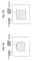
- the shape of the current passing-through region becomes asymmetrical (see FIG. 17A ), and it is difficult for the cross sectional shape of the output laser beam to be a circle.
- FIG. 17B a current passing-through region whose shape is symmetrical for two axes is shown.
- the inventors of the present invention have studied a relationship between a shape of a current passing-through region, and a polarization suppression ratio and a radiation angle of an output laser beam in detail by manufacturing a surface emitting laser element having an inclined substrate. As a result, the inventors have newly found the following. That is, in some cases, it is difficult for a cross sectional shape of an output laser beam to be a circle, by only causing the shape of the current passing-through region to be a circle or a square.
- the inventors have studied the reasons of the above results in detail and have newly found that the thickness of an oxide surrounding the current passing-through region greatly influences the radiation angle of the output laser beam when an inclined substrate is used.
- a surface emitting laser element which emits laser beams in a direction perpendicular to a surface of a substrate of the surface emitting laser element, a surface emitting laser array in which the surface emitting laser elements are arrayed, an optical scanning device using the surface emitting laser element or the surface emitting laser array, and an image forming apparatus using the optical scanning device, in which stability in a polarization direction of the output laser beams can be obtained without causing high cost and a cross sectional shape of output laser beams can be substantially a circle.
- a surface emitting laser element which emits laser beams in a direction perpendicular to a surface of a substrate of the surface emitting laser element
- a surface emitting laser array in which the surface emitting laser elements are arrayed
- an optical scanning device using the surface emitting laser element or the surface emitting laser array
- an image forming apparatus using the optical scanning device particularly pointed out in the specification in such full, clear, concise, and exact terms so as to enable a person having ordinary skill in the art to practice the invention.
- the surface emitting laser element includes a substrate whose normal direction of a principal surface is inclined to one direction of a [1 1 1] crystal orientation relative to one direction of a [1 0 0] crystal orientation, a resonator structural body including an active layer, first and second semiconductor distributed Bragg reflectors which sandwich the resonator structural body and include a confinement structure in which a current passing-through region is surrounded by an oxidized layer, a plurality of semiconductor layers stacked on the substrate, and a metal layer having an opening part which becomes a light outputting section on the plural semiconductor layers.
- a laser beam whose cross sectional shape has a long length direction is input to the metal layer via the oxide confinement structure, and an opening width of the light outputting section in a first direction orthogonal to the long length direction of the laser beam is smaller than another opening width of the light outputting section in a second direction parallel to the long length direction of the laser beam.
- FIGs. 1 through 11 an embodiment of the present invention is described.
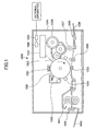
- FIG. 1 is a cut-away side view of an image forming apparatus according to the embodiment of the present invention.
- a laser printer 1000 is shown as the image forming apparatus.
- the laser printer 1000 includes an optical scanning device 1010, a photoconductor drum 1030, a charger 1031, a developing roller 1032, a transfer charger 1033, a discharging unit 1034, a cleaning unit 1035, a toner cartridge 1036, a paper feeding roller 1037, a paper feeding tray 1038, a pair of registration rollers 1039, fixing rollers 1041, paper outputting rollers 1042, a paper outputting tray 1043, a communication controller 1050, and a printer controller 1060 for totally controlling the above elements at corresponding predetermined positions in a printer cabinet 1044.
- the communication controller 1050 controls interactive communications with an external apparatus (for example, a personal computer) via, for example, a network.
- an external apparatus for example, a personal computer
- the photoconductor drum 1030 (image carrier) is a cylinder-shaped member and a photoconductor layer is formed on the surface of the photoconductor drum 1030. That is, the surface of the photoconductor drum 1030 is a surface to be scanned.
- the photoconductor drum 1030 is rotated in the arrow direction shown in FIG. 1 .
- the charger 1031, the developing roller 1032, the transfer charger 1033, the discharging unit 1034, and the cleaning unit 1035 are disposed near the surface of the photoconductor drum 1030.
- the charger 1031, the developing roller 1032, the transfer charger 1033, the discharging unit 1034, and the cleaning unit 1035 are sequentially disposed along the rotation direction of the photoconductor drum 1030 in this order.
- the charger 1031 uniformly charges the surface of the photoconductor drum 1030.
- the optical scanning device 1010 radiates a light flux (laser beam) modulated based on image information transmitted from the external apparatus onto the surface of the photoconductor drum 1030 charged by the charger 1031. With this, an electrostatic latent image based on the image information is formed onto the surface of the photoconductor drum 1030. The formed electrostatic latent image is moved to the developing roller 1032 corresponding to the rotation of the photoconductor drum 1030.
- the optical scanning device 1010 is described below in detail.
- Toners are stored in the toner cartridge 1036 and the stored toners are supplied to the developing roller 1032.
- the developing roller 1032 adheres the toners supplied from the toner cartridge 1036 onto the electrostatic latent image formed on the surface of the photoconductor drum 1030. With this, the electrostatic latent image is developed and the image information is caused to appear.
- the electrostatic latent image on which the toners are adhered (toner image) is moved to the transfer charger 1033 corresponding to the rotation of the photoconductor drum 1030.
- Recording paper 1040 is stored in the paper feeding tray 1038.
- the paper feeding roller 1037 which is disposed near the paper feeding tray 1038, picks up the recording paper 1040 one by one from the paper feeding tray 1038, and transports the picked up recording paper 1040 to the pair of the registration rollers 1039.
- the pair of the registration rollers 1039 temporarily holds the recording paper 1040 picked up by the paper feeding roller 1037 and transports the recording paper 1040 to a position (gap) between the photoconductor drum 1030 and the transfer charger 1033 corresponding to the rotation of the photoconductor drum 1030.
- a voltage whose polarity is reverse to the polarity of the toners is applied onto the transfer charger 1033 so that the toner image on the photoconductor drum 1030 is electrically attracted onto the recording paper 1040.
- the toner image on the surface of the photoconductor drum 1030 is transferred onto the recording paper 1040 by the voltage.
- the recording paper 1040 onto which the toner image has been transferred is transported to the fixing rollers 1041.
- Heat and pressure are applied to the recording paper 1040 by the fixing rollers 1041. With this, the toner image on the recording paper 1040 is fixed.
- the recording paper 1040 on which the toner image has been fixed by the fixing rollers 1041 is transported to the paper outputting tray 1043 via the paper outputting rollers 1042, and the recording paper 1040 is stacked on the paper outputting tray 1043.
- the discharging unit 1034 discharges the surface of the photoconductor drum 1030.
- the cleaning unit 1035 removes the toners remaining on the surface of the photoconductor drum 1030.
- the surface of the photoconductor drum 1030 on which the remaining toners have been removed returns to a position to face the charger 1031.
- FIG. 2 is a cut-away side view of the optical scanning device 1010.
- the optical scanning device 1010 includes a deflector side scanning lens 11a, an image face side scanning lens 11b, a polygon mirror 13 (deflecting unit), a light source 14, a coupling lens 15, an aperture plate 16, an anamorphic lens 17, a reflection mirror 18, and a scanning controller (not shown) at corresponding predetermined positions in housing 30.
- the direction corresponding to the main scanning direction is called the main scanning corresponding direction and the direction corresponding to the sub scanning direction is called the sub scanning corresponding direction.
- the coupling lens 15 causes the light flux (laser beam) output from the light source 14 to be approximately parallel light.
- the light source 14 and the coupling lens 15 are secured to a supporting member formed of aluminum and are integrated together.
- the aperture plate 16 includes an aperture section and controls the beam diameter of the light flux sent from the coupling lens 15.
- the anamorphic lens 17 forms an image near the deflection reflection surface of the polygon mirror 13 from the light flux passed through the aperture section of the aperture plate 16 via the reflection mirror 18 in the sub scanning corresponding direction.
- optical system before deflector An optical system disposed on an optical route between the light source 14 and the polygon mirror 13 is called an optical system before deflector.
- the optical system before deflector is formed of the coupling lens 15, the aperture plate 16, the anamorphic lens 17, and the reflection mirror 18.
- the polygon mirror 13 has a six-sided mirror whose inscribing circle radius is, for example, 18 mm and each mirror is a deflection reflection surface.
- the polygon mirror 13 rotates at a constant speed around an axle parallel to the sub scanning corresponding direction and deflects the light flux from the reflection mirror 18.
- the deflector side scanning lens 11a is in the optical route of the light flux deflected by the polygon mirror 13.
- the image face side scanning lens 11b is in the optical route from the deflector side scanning lens 11a.
- the light flux from the image face side scanning lens 11b is radiated onto the surface of the photoconductor drum 1030, and a light spot is formed on the surface of the photoconductor drum 1030.
- the light spot moves in the long length direction (the width direction) of the photoconductor drum 1030 corresponding to the rotation of the polygon mirror 13. That is, the light spot scans the surface of the photoconductor drum 1030.
- the moving direction of the light spot is the main scanning direction, and the rotation direction of the photoconductor drum 1030 is the sub scanning direction.
- An optical system on an optical route between the polygon mirror 13 and the photoconductor drum 1030 is called a scanning optical system.
- the scanning optical system is formed of the deflector side scanning lens 11a and the image face side scanning lens 11b.
- at least one optical axis folding mirror can be disposed on at least one of the optical route between the deflector side scanning lens 11a and the image face side scanning lens 11b, and the optical route between the image face side scanning lens 11b and the photoconductor drum 1030.
- FIG. 3A is a cut-away side view of a surface emitting laser element 100 according to the embodiment of the present invention.
- FIG. 3B is a top view of the surface emitting laser element 100.
- the light source 14 includes the surface emitting laser element 100 shown in FIGs. 3A and 3B .
- the laser beam (light flux) radiating direction is a Z axis direction, and two directions orthogonal to each other on a surface perpendicular to the Z axis direction are an X axis direction and a Y axis direction, respectively.
- a designed oscillation wavelength of the surface emitting laser element 100 is in a 780 nm band.
- the surface emitting laser element 100 includes a substrate 101, a buffer layer 102, a lower semiconductor DBR (distributed Bragg reflector) 103, a lower spacer layer 104, an active layer 105, an upper spacer layer 106, an upper semiconductor DBR 107, a contact layer 109, and so on.
- DBR distributed Bragg reflector
- FIGs. 3A and 3B elements having corresponding reference numbers 108, 108a, 108b, 112, 113, 114, and 115 are described below.
- FIG. 4A is a diagram showing an inclination of the substrate 101.
- FIG. 4B is a diagram showing a position of the substrate 101.
- the surface of the substrate 101 is a mirror polished surface, and the substrate 101 is an n-GaAs single crystal substrate.
- the substrate 101 is disposed so that the [0 1 -1] crystal orientation direction is the -X direction, and the [0 -1 1] crystal orientation direction is the +X direction.
- the buffer layer 102 is stacked on a +Z side surface of the substrate 101 and is formed of n-GaAs.
- the lower semiconductor DBR 103 is stacked at the +Z side of the buffer layer 102 and includes 40.5 pairs of a low refractive index layer formed of n-AlAs and a high refractive index layer formed of n-Al 0.3 Ga 0.7 As.
- a composition gradient layer of 20 nm thickness is formed between the refractive index layers in which the composition is gradually changed from one composition to the other composition.
- Each of the refractive index layers is determined to have an optical thickness of ⁇ /4 by including 1/2 of the adjacent composition gradient layers when the oscillation wavelength is ⁇ .
- the optical thickness is ⁇ /4
- the actual thickness "h" ⁇ /4N (N is the refractive index of a medium of the layer).
- the lower spacer layer 104 is stacked at the +Z side of the lower semiconductor DBR 103 and is formed of non-doped (Al 0.1 Ga 1.9 ) 0.5 In 0.5 P.
- the active layer 105 is stacked at the +Z side of the lower spacer layer 104 and has a triple quantum well structure having quantum well layers of three layers and barrier layers of four layers.
- Each of the quantum well layers is formed of GaInAsP whose composition induces a compression strain of 0.7%, and has a band gap wavelength of approximately 780 nm.
- Each of the barrier layers is formed of GaInP whose composition induces a tensile strain of 0.6%.
- the upper spacer layer 106 is stacked at the +Z side of the active layer 105 and is formed of non-doped (Al 0.1 Ga 0.9 ) 0.5 In 0.5 P.
- a part formed of the lower spacer layer 104, the active layer 105, and the upper spacer layer 106 is called a resonator structural body, and the thickness of the resonator structural body is determined to be the optical thickness of one wavelength.
- the active layer 105 is at a center of the resonator structural body which center corresponds to an anti-node position of a standing wave distribution of an electric field.
- the upper semiconductor DBR 107 includes a first upper semiconductor DBR (not shown) and a second upper semiconductor DBR (not shown).
- the first upper semiconductor DBR is stacked at the +Z side of the upper spacer layer 106 and includes a pair of a low refractive index layer formed of p-(Al 0.7 Ga 0.3 ) 0.5 In 0.5 P and a high refractive index layer formed of p-(Al 0.1 Ga 0.9 ) 0.5 In 0.5 P.
- the second upper semiconductor DBR is stacked at the +Z side of the first upper semiconductor DBR and includes 23 pairs of a low refractive index layer formed of p-Al 0.9 Ga 0.1 As and a high refractive index layer formed of p-Al 0.3 Ga 0.7 As.
- a composition gradient layer is formed between the refractive index layers of the upper semiconductor DBR 107 in which the composition is gradually changed from one composition to the other composition.
- Each of the low and high refractive index layers is determined to have an optical thickness of ⁇ /4 by including 1/2 of the adjacent composition gradient layers when the oscillation wavelength is ⁇ .
- a layer to be selectively oxidized 108 of 30 nm thickness formed of p-AlAs is inserted into one of the low refractive index layers of the second upper semiconductor DBR.
- the inserting position of the layer to be selectively oxidized 108 is in a 3 rd pair of the low refractive index layers from the upper spacer layer 106 and at a position corresponding to a node of a standing wave distribution of an electric field.
- the contact layer 109 is stacked at the +Z side of the second upper semiconductor DBR and is formed of p-GaAs.
- a structure in which plural semiconductor layers are stacked on the substrate 101 is called a layer stacked body.
- the polarization direction of the output laser beam is the X axis direction which is a desirable direction, and the polarization suppression ratio is 20 dB or more and stable.
- the polarization suppression ratio is a ratio of light intensity in the desirable polarization direction to light intensity in the direction orthogonal to the desirable polarization direction, and it is said that an image forming apparatus such as a copying apparatus is required to have approximately 20 dB.
- a difference between the radiation angles of the output laser beams in the X axis direction and the Y axis direction is 0.1 ° or less, and the cross sectional shape of the output laser beam is substantially circular.
- FIG. 6 is a cut-away side view of the surface emitting laser element 100 along line A-A of FIG. 3A . That is, an oxide confinement structure of the surface emitting laser element 100 is shown in FIG. 6 . In FIG. 6 , the followings are defined.
- a distance from the +Y side end of the oxidized layer 108a to the +Y side end of the current passing-through region 108b is "dy1"
- a distance from the -Y side end of the oxidized layer 108a to the -Y side end of the current passing-through region 108b is "dy2”
- a distance from the +X side end of the oxidized layer 108a to the +X side end of the current passing-through region 108b is "dx1”
- a distance from the -X side end of the oxidized layer 108a to the -X side end of the current passing-through region 108b is "dx2".
- the measured results are dy2 > dy1, and dx2 ⁇ dx1 > dy1. This shows that the oxidization rate in the -Y direction is smaller than the oxidization rates in the +Y, +X, and -X directions.
- a width of the current passing-through region 108b in the Y axis direction is "bY”
- FIG. 7 is a cut-away side view of the oxide confinement structure shown in FIG. 6 along line A-A of FIG. 6 .
- the followings are defined. That is, the thickness of the oxidized layer 108a at the +Y side of the current passing-through region 108b is "Sy1", and the thickness of the oxidized layer 108a at the -Y side of the current passing-through region 108b is "Sy2". Then when the thicknesses are measured at several positions in the Y axis direction, "Sy1" is greater than "Sy2" by approximately 2 nm even if the distances from the oxidation end parts are the same, for example, at the distances of "d” in FIG. 7 .
- FIG. 8 is a cut-away side view of the oxide confinement structure shown in FIG. 6 along line B-B of FIG. 6 .
- the followings are defined. That is, the thickness of the oxidized layer 108a at the -X side of the current passing-through region 108b is "Sx1", and the thickness of the oxidized layer 108a at the +X side of the current passing-through region 108b is "Sx2". Then when the thicknesses are measured at several positions in the X axis direction, "Sx1" is substantially equal to "Sx2" when the distances from the oxidation end parts are the same, for example, at the distances of "d” in FIG. 8 . In addition, the thicknesses of "Sx1" and “Sx2" are smaller than the thickness of "Sy1" even if the distance from the oxidation end part is the same.
- the inventors of the present invention have manufactured plural surface emitting laser elements 100 whose rectangular ratios of the current passing-through regions 108b are different from each other, and have obtained a relationship between the rectangular ratio and the polarization suppression ratio.
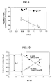
- FIG. 9 is a graph showing the relationship between the rectangular ratio (bY/bX) of the current passing-through region 108b and the polarization suppression ratio in the manufactured surface emitting laser elements 100.
- the polarization directions of the surface emitting laser elements 100 are the X axis direction; that is, the same direction.
- black circles show plural surface emitting laser elements of a first group and white circles show plural surface emitting laser elements of a second group and structures of the first and second groups are partially different from each other. As shown in FIG.
- the radiation angle of the output laser beam tends to be great when light confinement in the lateral direction (hereinafter, in some cases, simply referred to as light confinement) is great.
- the degree of the light confinement becomes great when the width of the current passing-through region is small and the thickness of the oxidized layer is great. That is, when the width of the current passing-through region is small and the thickness of the oxidized layer is great, the radiation angle of the output laser beam tends to become great.
- FIG. 10 is a graph showing a relationship between the rectangular ratio of the current passing-through region and the radiation angle of the output laser beam of a surface emitting laser element using an inclined substrate similar to the substrate 101 in which the shape of the light outputting section is square.
- the rectangular ratio (bY/bX) of the current passing-through region becomes great, the radiation angle in the X axis direction becomes great, and the radiation angle in the Y axis direction becomes small.
- the rectangular ratio (bY/bX) of the current passing-through region is approximately 1.1, the radiation angles in the X and Y axes direction become the same.
- the cross sectional shape of the output laser beam is ellipsoidal in which the Y axis direction is the long length direction.
- the cross sectional shape of the output laser beam is ellipsoidal in which the X axis direction is the long length direction.
- the rectangular ratio of the current passing-through region is less than approximately 1.1, the smaller the rectangular ratio of the current passing-through region is, the greater the difference between the radiation angles in the X axis direction and the Y axis direction is (hereinafter, in some cases, simply referred to as a radiation angle difference).
- the rectangular ratio of the current passing-through region is made to be small.
- the rectangular ratio of the current passing-through region is made to be less than 1.0, a higher polarization suppression ratio can be obtained than a conventional case is.
- the rectangular ratio of the current passing-through region is made to be less than 1.0, the radiation angle difference becomes larger than a conventional case is.
- the radiation angle difference is approximately 0.2 °
- the radiation angle difference is approximately 0.4 ° (see ⁇ r1 in FIG. 10 ).
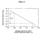
- FIG. 11 is a graph showing a relationship between an opening width of the light outputting section and an radiation angle of an output laser beam in the X axis direction of a surface emitting laser element using an inclined substrate similar to the substrate 101 in which the shapes of the light outputting section and the current passing-through region are square.
- the radiation angle of the output laser beam depends on the opening width of the light outputting section.
- the radiation angle of the output laser beam tends to become large. This tendency is the same as the radiation angle in the Y axis direction.
- the long length direction of the cross sectional shape of the output laser beam can be determined to be the X axis direction or the Y axis direction, by using a magnitude relation between the opening widths of the light outputting section in the X and Y axes directions.
- the size of the radiation angle difference can be adjusted by a difference (absolute value) between the opening widths of the light outputting section in the X axis direction and the Y axis direction.
- the opening widths in the X and Y axes directions are determined so that the opening width in the X axis direction is smaller than the opening width in the Y axis direction, "the radiation angle in the X axis direction > the radiation angle in the Y axis direction", and the size of the radiation angle difference is to be a value ( ⁇ r2 in FIG. 11 ) approximated to the value ⁇ r1.
- the opening width in the X axis direction is determined to be 10.0 ⁇ m
- the opening width in the Y axis direction is determined to be 11.5 ⁇ m.
- the cross sectional shape of the output laser beam can be substantially circular.
- the resonator structural body including the active layer 105 and the plural semiconductor layers including the lower semiconductor DBR 103 and the upper semiconductor DBR 107 sandwiching the resonator structural body are stacked.
- the rectangular ratio of the current passing-through region 108b is 0.89, and in the oxidized layer 108a surrounding the current passing-through region 108b, the oxidized thickness in the +Y direction is greater than in the +X, and -X directions.
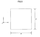
- the shape of the current passing-through region 108b is symmetrical for an axis (first axis) which passes through the center of the current passing-through region 108b and is parallel to the X axis and is symmetrical for another axis (second axis) which passes through the center of the current passing-through region 108b and is parallel to the Y axis.
- the opening width in the X axis direction is smaller than the opening width in the Y axis direction.
- the stability of the output laser beam in the polarization direction can be increased without causing high cost, and the cross sectional shape of the output laser beam can be substantially circular.
- the optical scanning device 1010 of the present embodiment since the light source 14 includes the surface emitting laser element 100, high accurate optical scanning can be performed without causing high cost.
- the laser printer 1000 of the present embodiment since the laser printer 1000 includes the optical scanning device 1010, a high quality image can be formed without causing high cost.
- the rectangular ratio of the current passing-through region 108b is 0.89 and the thickness of the oxidized layer 108a is non-uniform.
- the case is not limited to the above in the present embodiment.
- the present embodiment can be applied to a case in which the rectangular ratio of the current passing-through region 108b is 1.0 and the thickness of the oxidized layer 108a is non-uniform, and another case in which the rectangular ratio of the current passing-through region 108b is less than 1.0 and the thickness of the oxidized layer 108a is uniform.
- the oscillation wavelength of the surface emitting laser element 100 is in the 780 nm band.
- the oscillation wavelength of the surface emitting laser element 100 can be changed corresponding to the characteristics of the photoconductor body (photoconductor drum).
- the surface emitting laser element 100 can be used in an apparatus other than the image forming apparatus.
- the oscillation wavelength can be in a 650 nm band, a 850 nm band, a 980 nm band, a 1.3 ⁇ m band, a 1,5 ⁇ m band, and so on depending on the intended use.
- the semiconductor material for forming the active layer 105 a mixed crystal semiconductor material can be used corresponding to the oscillation wavelength.
- a mixed crystal semiconductor material based on AlGaInP when the oscillation wavelength is in the 650 nm band, a mixed crystal semiconductor material based on AlGaInP can be used, when the oscillation wavelength is in the 980 nm band, a mixed crystal semiconductor material based on InGaAs can be used, and when the oscillation wavelength is in the 1.3 ⁇ m or 1.5 ⁇ m band, a mixed crystal semiconductor material based on GaInNAs(Sb) can be used.
- each semiconductor DBR when a material and a structure of each semiconductor DBR is selected corresponding to the oscillation wavelength, a surface emitting laser element corresponding to an arbitrary oscillation wavelength can be formed.
- a material of the semiconductor DBR a mixed crystal material based on AlGaInp other than the mixed crystal material based on AlGaAs can be used. It is desirable that the low and high refractive index layers are transmittable for the oscillation wavelength, and a refractive index difference between the low and high refractive index layers is as large as possible.
- the shape of the light outputting section 115 of the surface emitting laser element 100 can be symmetrical for the axis which passes through the center of the light outputting section 115 and parallel to the Y axis direction, and can be asymmetrical for the axis which passes through the center of the light outputting section 115 and parallel to the X axis direction.
- the opening width of the light outputting section 115 at the +Y side can be greater than the opening width at the -Y side.
- FIG. 12A is a diagram showing the shapes of the laser beam and the current passing-through region 108b.
- the distortion of the shape of the laser beam generates a beam intensity distribution which is asymmetrical for the X axis direction; therefore, when a laser beam emitted from a surface emitting laser element passes through an opening part of an aperture plate, the light amount distribution of the laser beams passed through the opening part becomes asymmetrical for the X axis direction. However, when it is adjusted that the opening width at the +Y side is greater than at the -Y side in the light outputting section, the distortion of the shape of the laser beam can be corrected.
- the shape of the light outputting section 115 is preferably trapezoidal which can be easily designed and manufactured.
- FIG. 12B is a diagram showing the shapes of a laser beam and the light outputting section 115.
- the shape of the laser beam is slightly large in the +Y side, horizontally long, and has an asymmetrical distortion in the Y axis direction with the reflection of the distortion of the shape of the laser beam in the oxide confinement structure.
- the shape of the laser beam can be approximately circular having a low distortion.
- the shape of the laser beam can be a substantially circle.
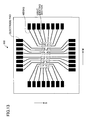
- FIG. 13 is a diagram showing a surface emitting laser array 500 according to the embodiment of the present invention.
- the light source 14 in the optical scanning device 1010 shown in FIG. 2 can include the surface emitting laser array 500 shown in FIG. 13 instead of including the surface emitting laser element 100.
- plural light emitting sections are disposed on a substrate.
- 32 light emitting sections are disposed.
- the M direction is the main scanning corresponding direction and the S direction is the sub scanning corresponding direction.
- the number of the light emitting sections is not limited to 32, and can be less than 32 or more than 32.
- FIG. 14 is a diagram showing a two-dimensional array of the light emitting sections shown in FIG. 13 .
- the surface emitting laser array 500 includes four light emitting section arrays in which eight light emitting sections are disposed with the same interval between the light emitting sections in the T direction having a tilt angle from the M direction toward the S direction.
- the eight light emitting sections in one array are disposed so that the interval in the S direction between the centers of the eight light emitting sections is "c" and the four light emitting section arrays are disposed so that the interval in the S direction between the four light emitting section arrays is "e" (distance between the centers of the two light emitting section arrays). That is, the 32 light emitting sections are two-dimensionally arrayed.
- the interval "c" is 3 ⁇ m
- the interval “e” is 24 ⁇ m
- the interval "m” between the light emitting sections in the M direction is 30 ⁇ m.
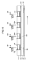
- FIG. 15 is a cut-away side view along line A-A of FIG. 14 .
- the light emitting section is the same as the surface emitting laser element 100. That is, the surface emitting laser array 500 can be manufactured by a method similar to the manufacturing method of the surface emitting laser element 100.
- the surface emitting laser array 500 is formed of the surface emitting laser elements 100. Therefore, the surface emitting laser array 500 can have the same effects as the effects of the surface emitting laser element 100.
- the interval "c" between the light emitting sections is constant when each of the light emitting sections is normally projected on a virtual line extending in the sub scanning corresponding direction; therefore, when light emitting timing of the light emitting sections is adjusted, it can be said that the light emitting sections are arrayed with the same interval on the photoconductor drum 1030 in the sub scanning direction.
- the interval "c" is 3 ⁇ m, when the magnification of the optical system of the optical scanning device 1010 is determined to be approximately 1.8 times, high density writing of 4800 dpi (dot per inch) can be performed.
- the number of the light emitting sections is increased in the main scanning corresponding direction, an array arrangement is performed in which the interval "c" is further decreased by narrowing the interval "e", or the magnification of the optical system is decreased; further high density writing can be performed, and higher quality printing can be performed.
- the writing interval in the main scanning direction can be easily controlled by adjusting the light emitting timing of the light emitting sections.
- the printing can be performed without decreasing the printing speed. Further, when the writing dot density is not changed, the printing speed can be further increased.
- the laser printer 1000 can stably form a high quality image.
- the distance (groove) between the two adjacent light emitting sections (the surface emitting laser elements 100) is preferably 5 ⁇ m or more so that the light emitting sections are electrically and spatially separated from each other. When the distance is too small, etching is not easily controlled when the surface emitting laser array 500 is manufactured.
- the size of the mesa (the length of one side) is preferably 10 ⁇ m or more. When the length is too short, heat stays inside the surface emitting array 500 and the characteristics may be lowered.
- surface emitting laser elements having a structure similar to the structure of the surface emitting laser elements 100 can be arrayed one-dimensionally.
- the normal direction of the mirror polished surface (principal surface) of the substrate 101 is inclined by 15 degrees to the [1 1 1] A crystal orientation direction relative to the [1 0 0] crystal orientation direction.
- the normal direction of the mirror polished surface (principal surface) of the substrate 101 can be inclined by a degree other than 15 degrees in the [1 1 1] A crystal orientation direction relative to the [1 0 0] crystal orientation direction.
- the laser printer 1000 is used; however, the image forming apparatus is not limited to the laser printer 1000, and can be an image forming apparatus including the optical scanning device 1010.
- an image forming apparatus in which laser beams indicating corresponding colors are directly radiated onto a recording medium.
- an image forming apparatus can be used in which a silver salt film is used as an image carrier.
- a latent image is formed on the silver salt film by optical scanning, and the latent image can be visualized by a developing process of a normal silver salt photographic process.
- the visible image can be transferred onto photographic printing paper by a printing process of the normal silver salt photographic process.
- the image forming apparatus can be used as an optical reproduction apparatus or an optical image forming apparatus which shows a CT (computerized tomography) scanned image and so on.
- FIG. 16 is a cut-away side view of the color printer 2000.
- the color printer 2000 is a tandem type multiple color printer which forms a full color image by superposing four color images (black, cyan, magenta, and yellow images).
- the color printer 2000 includes a photoconductor drum K1, a charging device K2, a developing device K4, a cleaning unit K5, and a transfer device K6 for a black image; a photoconductor drum C1, a charging device C2, a developing device C4, a cleaning unit C5, and a transfer device C6 for a cyan image; a photoconductor drum M1, a charging device M2, a developing device M4, a cleaning unit M5, and a transfer device M6 for a magenta image; a photoconductor drum Y1, a charging device Y2, a developing device Y4, a cleaning unit Y5, and a transfer device Y6 for a yellow image; an optical scanning device 2010, a transfer belt 2080, a fixing unit 2030, and so on.
- the photoconductor drum K1 is rotated in the arrow direction shown in FIG. 16 .
- the charging device K2, the developing device K4, the transfer device K6, and the cleaning unit K5 are sequentially disposed to surround the photoconductor drum K1 along the rotational direction of the photoconductor drum K1.
- the charging device K2 uniformly charges the surface of the photoconductor drum K1.
- the optical scanning device 2010 radiates laser beams onto the surface of the photoconductor drum K1 charged by the charging device K2. With this, an electrostatic latent image is formed on the surface of the photoconductor drum K1.
- the developing device K4 develops the electrostatic latent image and forms a toner image on the surface of the photoconductor drum K1.
- the transfer device K6 transfers the toner image onto a recording medium (paper) on a transfer belt 2080, and the transferred image is fixed by the fixing unit 2030. When the above operations are performed for all color images, a full color image is printed on the recording medium.
- the optical scanning device 2010 includes a light source similar to the light source 14 in each color. Therefore, the optical scanning device 2010 can obtain the same effects as those of the optical scanning device 1010. In addition, since the color printer 2000 includes the optical scanning device 2010, the color printer 2000 can obtain the same effects as those of the laser printer 1000.
- a color registration error may be generated due to a manufacturing error of each component and a positioning error of the component.
- each of the light sources of the optical scanning device 2010 includes a surface emitting laser array similar to the surface emitting laser array 500, when a light emitting section to be lighted is selected, the color registration error can be decreased.
- the stability of the output laser beam in the polarization direction can be high and the cross sectional shape of the output laser beam can be substantially circular without causing high cost.
- the optical scanning device 1010 (2010) accurate optical scanning can be performed without causing high cost.
- the image forming apparatus 1000 (2000) can form a high quality image without causing high cost.
- the present invention is based on Japanese Priority Patent Application No. 2008-153382, filed on June 11, 2008 , and Japanese Priority Patent Application No. 2009-092551, filed on April 7, 2009 , with the Japanese Patent Office, the entire contents of which are hereby incorporated herein by reference.
Landscapes
- Physics & Mathematics (AREA)
- General Physics & Mathematics (AREA)
- Condensed Matter Physics & Semiconductors (AREA)
- Electromagnetism (AREA)
- Optics & Photonics (AREA)
- Semiconductor Lasers (AREA)
- Mechanical Optical Scanning Systems (AREA)
- Laser Beam Printer (AREA)
Applications Claiming Priority (2)
| Application Number | Priority Date | Filing Date | Title |
|---|---|---|---|
| JP2008153382 | 2008-06-11 | ||
| JP2009092551A JP5316784B2 (ja) | 2008-06-11 | 2009-04-07 | 面発光レーザ素子、面発光レーザアレイ、光走査装置及び画像形成装置 |
Publications (3)
| Publication Number | Publication Date |
|---|---|
| EP2133965A2 true EP2133965A2 (de) | 2009-12-16 |
| EP2133965A3 EP2133965A3 (de) | 2011-02-09 |
| EP2133965B1 EP2133965B1 (de) | 2012-10-10 |
Family
ID=41077986
Family Applications (1)
| Application Number | Title | Priority Date | Filing Date |
|---|---|---|---|
| EP09251536A Not-in-force EP2133965B1 (de) | 2008-06-11 | 2009-06-11 | Oberflächenemittierendes Laserelement, oberflächenemittierendes Laserarray, optische Abtastvorrichtung und Bilderstellungsvorrichtung |
Country Status (6)
| Country | Link |
|---|---|
| US (1) | US7978739B2 (de) |
| EP (1) | EP2133965B1 (de) |
| JP (1) | JP5316784B2 (de) |
| KR (1) | KR101054948B1 (de) |
| CN (1) | CN101604819B (de) |
| TW (1) | TWI392178B (de) |
Cited By (1)
| Publication number | Priority date | Publication date | Assignee | Title |
|---|---|---|---|---|
| US10910226B2 (en) | 2016-10-28 | 2021-02-02 | Osram Oled Gmbh | Method of producing a semiconductor laser and semiconductor laser |
Families Citing this family (42)
| Publication number | Priority date | Publication date | Assignee | Title |
|---|---|---|---|---|
| JP5316783B2 (ja) * | 2008-05-15 | 2013-10-16 | 株式会社リコー | 面発光レーザ素子、面発光レーザアレイ、光走査装置及び画像形成装置 |
| JP5515767B2 (ja) | 2009-05-28 | 2014-06-11 | 株式会社リコー | 面発光レーザ素子の製造方法、面発光レーザ素子、面発光レーザアレイ、光走査装置及び画像形成装置 |
| JP5636686B2 (ja) | 2009-06-04 | 2014-12-10 | 株式会社リコー | 面発光レーザアレイ、光走査装置、画像形成装置、及び面発光レーザアレイの製造方法 |
| JP5510899B2 (ja) | 2009-09-18 | 2014-06-04 | 株式会社リコー | 面発光レーザ素子、面発光レーザアレイ、光走査装置、及び画像形成装置 |
| US8570649B2 (en) * | 2009-10-29 | 2013-10-29 | California Institute Of Technology | Dual-mode raster point scanning/light sheet illumination microscope |
| JP2011124541A (ja) * | 2009-11-12 | 2011-06-23 | Ricoh Co Ltd | 光デバイス、光走査装置及び画像形成装置、並びに光デバイスの製造方法 |
| JP5532321B2 (ja) * | 2009-11-17 | 2014-06-25 | 株式会社リコー | 面発光レーザ素子、面発光レーザアレイ、光走査装置及び画像形成装置 |
| JP5527714B2 (ja) * | 2009-11-18 | 2014-06-25 | 株式会社リコー | 面発光レーザ素子、面発光レーザアレイ、光走査装置及び画像形成装置 |
| JP5522595B2 (ja) * | 2009-11-27 | 2014-06-18 | 株式会社リコー | 面発光レーザ素子、面発光レーザアレイ、光走査装置及び画像形成装置 |
| JP2011151357A (ja) | 2009-12-21 | 2011-08-04 | Ricoh Co Ltd | 光デバイス、光走査装置及び画像形成装置 |
| JP2011159943A (ja) * | 2010-01-08 | 2011-08-18 | Ricoh Co Ltd | 面発光レーザ素子、面発光レーザアレイ、光走査装置及び画像形成装置 |
| JP2011166108A (ja) * | 2010-01-15 | 2011-08-25 | Ricoh Co Ltd | 面発光レーザ素子、面発光レーザアレイ、光走査装置及び画像形成装置 |
| JP5834414B2 (ja) | 2010-03-18 | 2015-12-24 | 株式会社リコー | 面発光レーザモジュール、光走査装置及び画像形成装置 |
| JP5585940B2 (ja) | 2010-04-22 | 2014-09-10 | 株式会社リコー | 面発光レーザ素子、面発光レーザアレイ、光走査装置、画像形成装置及び面発光レーザ素子の製造方法 |
| JP5601014B2 (ja) | 2010-04-23 | 2014-10-08 | 株式会社リコー | 光デバイス、光走査装置及び画像形成装置 |
| JP2011249763A (ja) | 2010-04-28 | 2011-12-08 | Ricoh Co Ltd | 光源ユニット、光走査装置及び画像形成装置 |
| JP5754624B2 (ja) | 2010-05-25 | 2015-07-29 | 株式会社リコー | 面発光レーザ素子、面発光レーザアレイ、光走査装置、画像形成装置及び面発光レーザ素子の製造方法 |
| JP5721055B2 (ja) | 2010-06-11 | 2015-05-20 | 株式会社リコー | 面発光レーザ素子、面発光レーザアレイ、光走査装置、画像形成装置及び面発光レーザ素子の製造方法 |
| CA2817190C (en) | 2010-11-26 | 2016-12-06 | Yoshihiro Ohba | Optical sensor and image forming apparatus |
| JP5783493B2 (ja) * | 2011-03-16 | 2015-09-24 | 株式会社リコー | 面発光レーザアレイとそれを用いた光走査装置と画像形成装置 |
| JP2012209534A (ja) | 2011-03-17 | 2012-10-25 | Ricoh Co Ltd | 面発光レーザ素子、原子発振器及び面発光レーザ素子の検査方法 |
| JP5929259B2 (ja) | 2011-05-17 | 2016-06-01 | 株式会社リコー | 面発光レーザ素子、光走査装置及び画像形成装置 |
| JP5999303B2 (ja) | 2011-06-24 | 2016-09-28 | 株式会社リコー | 面発光レーザアレイ及び画像形成装置 |
| JP2013051398A (ja) | 2011-08-01 | 2013-03-14 | Ricoh Co Ltd | 面発光レーザ素子、光走査装置及び画像形成装置 |
| JP6303255B2 (ja) | 2011-12-02 | 2018-04-04 | 株式会社リコー | 面発光レーザ素子及び原子発振器 |
| JP2013131509A (ja) | 2011-12-20 | 2013-07-04 | Ricoh Co Ltd | 光学ユニットの製造方法、光学ユニット、光走査装置及び画像形成装置 |
| JP5999304B2 (ja) | 2012-02-17 | 2016-09-28 | 株式会社リコー | 光学センサ及び画像形成装置 |
| JP5999305B2 (ja) | 2012-02-20 | 2016-09-28 | 株式会社リコー | 光学センサ及び画像形成装置 |
| JP5939461B2 (ja) | 2012-03-01 | 2016-06-22 | 株式会社リコー | 光学センサ及び画像形成装置 |
| JP6102525B2 (ja) | 2012-07-23 | 2017-03-29 | 株式会社リコー | 面発光レーザ素子及び原子発振器 |
| JP6107089B2 (ja) | 2012-11-30 | 2017-04-05 | 株式会社リコー | 面発光レーザ素子及び原子発振器 |
| JP6176298B2 (ja) * | 2015-09-03 | 2017-08-09 | 富士ゼロックス株式会社 | 面発光型半導体レーザアレイ及び面発光型半導体レーザアレイの製造方法 |
| JP7031856B2 (ja) * | 2018-02-14 | 2022-03-08 | 国立大学法人東京工業大学 | ビーム偏向デバイス |
| CN108616033A (zh) * | 2018-05-10 | 2018-10-02 | 中山大学 | 集成超表面于vcsel的轨道角动量发射器件及其制备方法 |
| CN109449751A (zh) * | 2018-12-29 | 2019-03-08 | 苏州长光华芯半导体激光创新研究院有限公司 | 外腔面光源vcsel及其应用 |
| CN109787086B (zh) * | 2019-01-23 | 2021-02-02 | 扬州乾照光电有限公司 | Vcsel阵列芯片及其制作方法 |
| US10985531B2 (en) * | 2019-01-27 | 2021-04-20 | Hewlett Packard Enterprise Development Lp | Intensity noise mitigation for vertical-cavity surface emitting lasers |
| CN110649466B (zh) * | 2019-11-26 | 2021-07-13 | 常州纵慧芯光半导体科技有限公司 | 一种vcsel阵列、制造方法、平顶远场生成方法及照明模组 |
| JP7434849B2 (ja) | 2019-11-29 | 2024-02-21 | 株式会社リコー | 面発光レーザ、面発光レーザ装置、光源装置及び検出装置 |
| CN111162451A (zh) * | 2019-12-26 | 2020-05-15 | 浙江博升光电科技有限公司 | 底部发射垂直腔面发射激光器 |
| US12562552B2 (en) * | 2021-08-23 | 2026-02-24 | Genesee Valley Innovations, LLC | Independently-addressable high power surface-emitting laser array with tight-pitch packing |
| CN116774190A (zh) * | 2023-08-17 | 2023-09-19 | 深圳市速腾聚创科技有限公司 | 发射模组、激光发射模块和激光雷达设备 |
Citations (7)
| Publication number | Priority date | Publication date | Assignee | Title |
|---|---|---|---|---|
| JPH0410095B2 (de) | 1982-05-14 | 1992-02-24 | ||
| JPH09172218A (ja) | 1995-10-31 | 1997-06-30 | Hewlett Packard Co <Hp> | 一定の偏光方向を有する垂直共振型面発光レーザー |
| JP2891133B2 (ja) | 1994-10-24 | 1999-05-17 | 日本電気株式会社 | 面発光レーザ及び面発光レーザアレイ及び光情報処理装置 |
| JP3762765B2 (ja) | 2002-12-18 | 2006-04-05 | 三星電子株式会社 | 垂直空洞表面放射レーザ及びその製造方法 |
| JP2008028424A (ja) | 2000-11-13 | 2008-02-07 | Fuji Xerox Co Ltd | 面発光型半導体レーザ |
| JP2008153382A (ja) | 2006-12-15 | 2008-07-03 | Hitachi Cable Ltd | 窒化物半導体の製造方法 |
| JP2009092551A (ja) | 2007-10-10 | 2009-04-30 | Konica Minolta Holdings Inc | 障害物計測方法、障害物計測装置及び障害物計測システム |
Family Cites Families (21)
| Publication number | Priority date | Publication date | Assignee | Title |
|---|---|---|---|---|
| JP3232152B2 (ja) | 1992-05-14 | 2001-11-26 | 株式会社リコー | 発光ダイオードアレイ |
| US5331654A (en) | 1993-03-05 | 1994-07-19 | Photonics Research Incorporated | Polarized surface-emitting laser |
| US5412680A (en) | 1994-03-18 | 1995-05-02 | Photonics Research Incorporated | Linear polarization of semiconductor laser |
| JPH08116130A (ja) * | 1994-10-19 | 1996-05-07 | Nec Corp | 面発光レーザ |
| JP3551718B2 (ja) * | 1997-08-18 | 2004-08-11 | 富士ゼロックス株式会社 | 面発光型半導体レーザ |
| JP3262765B2 (ja) | 1999-06-18 | 2002-03-04 | 東洋通信機株式会社 | 圧電発振器用シート基板の構造 |
| JP4010095B2 (ja) | 1999-10-01 | 2007-11-21 | 富士ゼロックス株式会社 | 面発光型半導体レーザ及びレーザアレイ |
| US7245647B2 (en) | 1999-10-28 | 2007-07-17 | Ricoh Company, Ltd. | Surface-emission laser diode operable in the wavelength band of 1.1-1.7mum and optical telecommunication system using such a laser diode |
| US6975663B2 (en) | 2001-02-26 | 2005-12-13 | Ricoh Company, Ltd. | Surface-emission laser diode operable in the wavelength band of 1.1-7μm and optical telecommunication system using such a laser diode |
| JP2002208755A (ja) * | 2000-11-13 | 2002-07-26 | Fuji Xerox Co Ltd | 面発光型半導体レーザ |
| US6650683B2 (en) | 2000-11-20 | 2003-11-18 | Fuji Xerox Co, Ltd. | Surface emitting semiconductor laser |
| JP2003152280A (ja) | 2001-11-14 | 2003-05-23 | Sony Corp | 半導体レーザ素子 |
| JP4212046B2 (ja) | 2003-03-20 | 2009-01-21 | 株式会社リコー | 指向性可変アンテナおよび該アンテナを用いた電子機器、ならびに該アンテナを用いたアンテナ指向性制御方法 |
| EP1496583B1 (de) | 2003-07-07 | 2016-05-18 | II-VI Laser Enterprise GmbH | Oberflächenemittierender Laser mit vertikalem Resonator mit verbesserter Kontrolle der transversalen Moden und Herstellungsverfahren desselben |
| JP4138629B2 (ja) * | 2003-11-06 | 2008-08-27 | 株式会社東芝 | 面発光型半導体素子及びその製造方法 |
| EP1780849B1 (de) | 2004-06-11 | 2013-01-30 | Ricoh Company, Ltd. | Oberflächenemissions-laserdiode und herstellungsverfahren dafür |
| JP2006269568A (ja) * | 2005-03-23 | 2006-10-05 | Fuji Photo Film Co Ltd | 半導体レーザ素子 |
| JP4839662B2 (ja) * | 2005-04-08 | 2011-12-21 | 富士ゼロックス株式会社 | 面発光半導体レーザアレイおよびそれを用いた光伝送システム |
| JP4885573B2 (ja) * | 2006-03-06 | 2012-02-29 | 株式会社リコー | 光走査装置および画像形成装置 |
| JP5442940B2 (ja) | 2006-08-23 | 2014-03-19 | 株式会社リコー | 面発光レーザアレイ、それを備えた光走査装置および画像形成装置 |
| JP5309485B2 (ja) | 2006-08-30 | 2013-10-09 | 株式会社リコー | 面発光レーザ、面発光レーザアレイ、光走査装置及び画像形成装置 |
-
2009
- 2009-04-07 JP JP2009092551A patent/JP5316784B2/ja not_active Expired - Fee Related
- 2009-06-09 US US12/481,080 patent/US7978739B2/en not_active Expired - Fee Related
- 2009-06-10 TW TW098119430A patent/TWI392178B/zh not_active IP Right Cessation
- 2009-06-11 KR KR1020090051979A patent/KR101054948B1/ko not_active Expired - Fee Related
- 2009-06-11 EP EP09251536A patent/EP2133965B1/de not_active Not-in-force
- 2009-06-11 CN CN2009101459432A patent/CN101604819B/zh not_active Expired - Fee Related
Patent Citations (7)
| Publication number | Priority date | Publication date | Assignee | Title |
|---|---|---|---|---|
| JPH0410095B2 (de) | 1982-05-14 | 1992-02-24 | ||
| JP2891133B2 (ja) | 1994-10-24 | 1999-05-17 | 日本電気株式会社 | 面発光レーザ及び面発光レーザアレイ及び光情報処理装置 |
| JPH09172218A (ja) | 1995-10-31 | 1997-06-30 | Hewlett Packard Co <Hp> | 一定の偏光方向を有する垂直共振型面発光レーザー |
| JP2008028424A (ja) | 2000-11-13 | 2008-02-07 | Fuji Xerox Co Ltd | 面発光型半導体レーザ |
| JP3762765B2 (ja) | 2002-12-18 | 2006-04-05 | 三星電子株式会社 | 垂直空洞表面放射レーザ及びその製造方法 |
| JP2008153382A (ja) | 2006-12-15 | 2008-07-03 | Hitachi Cable Ltd | 窒化物半導体の製造方法 |
| JP2009092551A (ja) | 2007-10-10 | 2009-04-30 | Konica Minolta Holdings Inc | 障害物計測方法、障害物計測装置及び障害物計測システム |
Non-Patent Citations (1)
| Title |
|---|
| T. OHTOSHI ET AL.: "Dependence of optical gain on crystal orientation in surface emitting lasers with strained quantum wells", APPL. PHYS. LETT., vol. 65, no. 15, 1994, pages 1886 - 1877 |
Cited By (2)
| Publication number | Priority date | Publication date | Assignee | Title |
|---|---|---|---|---|
| US10910226B2 (en) | 2016-10-28 | 2021-02-02 | Osram Oled Gmbh | Method of producing a semiconductor laser and semiconductor laser |
| US11935755B2 (en) | 2016-10-28 | 2024-03-19 | Osram Oled Gmbh | Method of producing a semiconductor laser and semiconductor laser |
Also Published As
| Publication number | Publication date |
|---|---|
| TWI392178B (zh) | 2013-04-01 |
| JP5316784B2 (ja) | 2013-10-16 |
| EP2133965A3 (de) | 2011-02-09 |
| US20090310632A1 (en) | 2009-12-17 |
| EP2133965B1 (de) | 2012-10-10 |
| JP2010021521A (ja) | 2010-01-28 |
| KR101054948B1 (ko) | 2011-08-05 |
| US7978739B2 (en) | 2011-07-12 |
| KR20090129374A (ko) | 2009-12-16 |
| CN101604819B (zh) | 2012-04-11 |
| TW201014094A (en) | 2010-04-01 |
| CN101604819A (zh) | 2009-12-16 |
Similar Documents
| Publication | Publication Date | Title |
|---|---|---|
| EP2133965B1 (de) | Oberflächenemittierendes Laserelement, oberflächenemittierendes Laserarray, optische Abtastvorrichtung und Bilderstellungsvorrichtung | |
| EP2120302B1 (de) | Oberflächenemittierendes Laserelement, oberflächenemittierendes Laserarray, optische Abtastvorrichtung und Bilderstellungsvorrichtung | |
| US8441511B2 (en) | Surface-emitting laser element including dielectric film selectively provided to control reflectance in emission region, surface-emitting laser array, optical scanner device, and image forming apparatus | |
| US8111725B2 (en) | Surface-emitting laser, surface-emitting laser array, optical scanning device, and image forming apparatus | |
| JP5261754B2 (ja) | 面発光レーザ素子、面発光レーザアレイ、光走査装置及び画像形成装置 | |
| KR101347963B1 (ko) | 면발광 레이저의 제조 방법, 면발광 레이저, 면발광 레이저 어레이, 광주사 장치, 및 화상 형성 장치 | |
| US8855159B2 (en) | Surface-emitting laser element, surface-emitting laser array, optical scanner device, and image forming apparatus | |
| US9046808B2 (en) | Surface emitting laser array and image forming apparatus | |
| JP6015982B2 (ja) | 面発光レーザ、光走査装置及び画像形成装置 | |
| JP5505614B2 (ja) | 面発光レーザ素子、面発光レーザアレイ、光走査装置及び画像形成装置 |
Legal Events
| Date | Code | Title | Description |
|---|---|---|---|
| PUAI | Public reference made under article 153(3) epc to a published international application that has entered the european phase |
Free format text: ORIGINAL CODE: 0009012 |
|
| 17P | Request for examination filed |
Effective date: 20090701 |
|
| AK | Designated contracting states |
Kind code of ref document: A2 Designated state(s): AT BE BG CH CY CZ DE DK EE ES FI FR GB GR HR HU IE IS IT LI LT LU LV MC MK MT NL NO PL PT RO SE SI SK TR |
|
| PUAL | Search report despatched |
Free format text: ORIGINAL CODE: 0009013 |
|
| AK | Designated contracting states |
Kind code of ref document: A3 Designated state(s): AT BE BG CH CY CZ DE DK EE ES FI FR GB GR HR HU IE IS IT LI LT LU LV MC MK MT NL NO PL PT RO SE SI SK TR |
|
| AX | Request for extension of the european patent |
Extension state: AL BA RS |
|
| RIC1 | Information provided on ipc code assigned before grant |
Ipc: H01S 5/183 20060101AFI20120321BHEP Ipc: H01S 5/042 20060101ALN20120321BHEP |
|
| GRAP | Despatch of communication of intention to grant a patent |
Free format text: ORIGINAL CODE: EPIDOSNIGR1 |
|
| RIC1 | Information provided on ipc code assigned before grant |
Ipc: B41J 2/47 20060101ALN20120330BHEP Ipc: B41J 2/455 20060101ALN20120330BHEP Ipc: G03G 15/00 20060101ALN20120330BHEP Ipc: H01S 5/042 20060101ALN20120330BHEP Ipc: H01S 5/183 20060101AFI20120330BHEP |
|
| GRAS | Grant fee paid |
Free format text: ORIGINAL CODE: EPIDOSNIGR3 |
|
| GRAA | (expected) grant |
Free format text: ORIGINAL CODE: 0009210 |
|
| AK | Designated contracting states |
Kind code of ref document: B1 Designated state(s): AT BE BG CH CY CZ DE DK EE ES FI FR GB GR HR HU IE IS IT LI LT LU LV MC MK MT NL NO PL PT RO SE SI SK TR |
|
| REG | Reference to a national code |
Ref country code: GB Ref legal event code: FG4D |
|
| REG | Reference to a national code |
Ref country code: AT Ref legal event code: REF Ref document number: 579330 Country of ref document: AT Kind code of ref document: T Effective date: 20121015 Ref country code: CH Ref legal event code: EP |
|
| REG | Reference to a national code |
Ref country code: IE Ref legal event code: FG4D |
|
| REG | Reference to a national code |
Ref country code: DE Ref legal event code: R096 Ref document number: 602009010322 Country of ref document: DE Effective date: 20121206 |
|
| PG25 | Lapsed in a contracting state [announced via postgrant information from national office to epo] |
Ref country code: SI Free format text: LAPSE BECAUSE OF FAILURE TO SUBMIT A TRANSLATION OF THE DESCRIPTION OR TO PAY THE FEE WITHIN THE PRESCRIBED TIME-LIMIT Effective date: 20121010 |
|
| REG | Reference to a national code |
Ref country code: NL Ref legal event code: VDEP Effective date: 20121010 |
|
| REG | Reference to a national code |
Ref country code: AT Ref legal event code: MK05 Ref document number: 579330 Country of ref document: AT Kind code of ref document: T Effective date: 20121010 |
|
| REG | Reference to a national code |
Ref country code: LT Ref legal event code: MG4D |
|
| PG25 | Lapsed in a contracting state [announced via postgrant information from national office to epo] |
Ref country code: LT Free format text: LAPSE BECAUSE OF FAILURE TO SUBMIT A TRANSLATION OF THE DESCRIPTION OR TO PAY THE FEE WITHIN THE PRESCRIBED TIME-LIMIT Effective date: 20121010 Ref country code: NL Free format text: LAPSE BECAUSE OF FAILURE TO SUBMIT A TRANSLATION OF THE DESCRIPTION OR TO PAY THE FEE WITHIN THE PRESCRIBED TIME-LIMIT Effective date: 20121010 Ref country code: IS Free format text: LAPSE BECAUSE OF FAILURE TO SUBMIT A TRANSLATION OF THE DESCRIPTION OR TO PAY THE FEE WITHIN THE PRESCRIBED TIME-LIMIT Effective date: 20130210 Ref country code: HR Free format text: LAPSE BECAUSE OF FAILURE TO SUBMIT A TRANSLATION OF THE DESCRIPTION OR TO PAY THE FEE WITHIN THE PRESCRIBED TIME-LIMIT Effective date: 20121010 Ref country code: FI Free format text: LAPSE BECAUSE OF FAILURE TO SUBMIT A TRANSLATION OF THE DESCRIPTION OR TO PAY THE FEE WITHIN THE PRESCRIBED TIME-LIMIT Effective date: 20121010 Ref country code: ES Free format text: LAPSE BECAUSE OF FAILURE TO SUBMIT A TRANSLATION OF THE DESCRIPTION OR TO PAY THE FEE WITHIN THE PRESCRIBED TIME-LIMIT Effective date: 20130121 Ref country code: SE Free format text: LAPSE BECAUSE OF FAILURE TO SUBMIT A TRANSLATION OF THE DESCRIPTION OR TO PAY THE FEE WITHIN THE PRESCRIBED TIME-LIMIT Effective date: 20121010 Ref country code: NO Free format text: LAPSE BECAUSE OF FAILURE TO SUBMIT A TRANSLATION OF THE DESCRIPTION OR TO PAY THE FEE WITHIN THE PRESCRIBED TIME-LIMIT Effective date: 20130110 |
|
| PG25 | Lapsed in a contracting state [announced via postgrant information from national office to epo] |
Ref country code: GR Free format text: LAPSE BECAUSE OF FAILURE TO SUBMIT A TRANSLATION OF THE DESCRIPTION OR TO PAY THE FEE WITHIN THE PRESCRIBED TIME-LIMIT Effective date: 20130111 Ref country code: PT Free format text: LAPSE BECAUSE OF FAILURE TO SUBMIT A TRANSLATION OF THE DESCRIPTION OR TO PAY THE FEE WITHIN THE PRESCRIBED TIME-LIMIT Effective date: 20130211 Ref country code: LV Free format text: LAPSE BECAUSE OF FAILURE TO SUBMIT A TRANSLATION OF THE DESCRIPTION OR TO PAY THE FEE WITHIN THE PRESCRIBED TIME-LIMIT Effective date: 20121010 Ref country code: BE Free format text: LAPSE BECAUSE OF FAILURE TO SUBMIT A TRANSLATION OF THE DESCRIPTION OR TO PAY THE FEE WITHIN THE PRESCRIBED TIME-LIMIT Effective date: 20121010 Ref country code: CY Free format text: LAPSE BECAUSE OF FAILURE TO SUBMIT A TRANSLATION OF THE DESCRIPTION OR TO PAY THE FEE WITHIN THE PRESCRIBED TIME-LIMIT Effective date: 20121010 Ref country code: PL Free format text: LAPSE BECAUSE OF FAILURE TO SUBMIT A TRANSLATION OF THE DESCRIPTION OR TO PAY THE FEE WITHIN THE PRESCRIBED TIME-LIMIT Effective date: 20121010 |
|
| PG25 | Lapsed in a contracting state [announced via postgrant information from national office to epo] |
Ref country code: AT Free format text: LAPSE BECAUSE OF FAILURE TO SUBMIT A TRANSLATION OF THE DESCRIPTION OR TO PAY THE FEE WITHIN THE PRESCRIBED TIME-LIMIT Effective date: 20121010 |
|
| PG25 | Lapsed in a contracting state [announced via postgrant information from national office to epo] |
Ref country code: BG Free format text: LAPSE BECAUSE OF FAILURE TO SUBMIT A TRANSLATION OF THE DESCRIPTION OR TO PAY THE FEE WITHIN THE PRESCRIBED TIME-LIMIT Effective date: 20130110 Ref country code: EE Free format text: LAPSE BECAUSE OF FAILURE TO SUBMIT A TRANSLATION OF THE DESCRIPTION OR TO PAY THE FEE WITHIN THE PRESCRIBED TIME-LIMIT Effective date: 20121010 Ref country code: SK Free format text: LAPSE BECAUSE OF FAILURE TO SUBMIT A TRANSLATION OF THE DESCRIPTION OR TO PAY THE FEE WITHIN THE PRESCRIBED TIME-LIMIT Effective date: 20121010 Ref country code: DK Free format text: LAPSE BECAUSE OF FAILURE TO SUBMIT A TRANSLATION OF THE DESCRIPTION OR TO PAY THE FEE WITHIN THE PRESCRIBED TIME-LIMIT Effective date: 20121010 Ref country code: CZ Free format text: LAPSE BECAUSE OF FAILURE TO SUBMIT A TRANSLATION OF THE DESCRIPTION OR TO PAY THE FEE WITHIN THE PRESCRIBED TIME-LIMIT Effective date: 20121010 |
|
| PLBE | No opposition filed within time limit |
Free format text: ORIGINAL CODE: 0009261 |
|
| STAA | Information on the status of an ep patent application or granted ep patent |
Free format text: STATUS: NO OPPOSITION FILED WITHIN TIME LIMIT |
|
| PG25 | Lapsed in a contracting state [announced via postgrant information from national office to epo] |
Ref country code: RO Free format text: LAPSE BECAUSE OF FAILURE TO SUBMIT A TRANSLATION OF THE DESCRIPTION OR TO PAY THE FEE WITHIN THE PRESCRIBED TIME-LIMIT Effective date: 20121010 Ref country code: IT Free format text: LAPSE BECAUSE OF FAILURE TO SUBMIT A TRANSLATION OF THE DESCRIPTION OR TO PAY THE FEE WITHIN THE PRESCRIBED TIME-LIMIT Effective date: 20121010 |
|
| 26N | No opposition filed |
Effective date: 20130711 |
|
| REG | Reference to a national code |
Ref country code: DE Ref legal event code: R097 Ref document number: 602009010322 Country of ref document: DE Effective date: 20130711 |
|
| PG25 | Lapsed in a contracting state [announced via postgrant information from national office to epo] |
Ref country code: MC Free format text: LAPSE BECAUSE OF FAILURE TO SUBMIT A TRANSLATION OF THE DESCRIPTION OR TO PAY THE FEE WITHIN THE PRESCRIBED TIME-LIMIT Effective date: 20121010 |
|
| REG | Reference to a national code |
Ref country code: CH Ref legal event code: PL |
|
| REG | Reference to a national code |
Ref country code: IE Ref legal event code: MM4A |
|
| PG25 | Lapsed in a contracting state [announced via postgrant information from national office to epo] |
Ref country code: IE Free format text: LAPSE BECAUSE OF NON-PAYMENT OF DUE FEES Effective date: 20130611 Ref country code: CH Free format text: LAPSE BECAUSE OF NON-PAYMENT OF DUE FEES Effective date: 20130630 Ref country code: LI Free format text: LAPSE BECAUSE OF NON-PAYMENT OF DUE FEES Effective date: 20130630 |
|
| PG25 | Lapsed in a contracting state [announced via postgrant information from national office to epo] |
Ref country code: MT Free format text: LAPSE BECAUSE OF FAILURE TO SUBMIT A TRANSLATION OF THE DESCRIPTION OR TO PAY THE FEE WITHIN THE PRESCRIBED TIME-LIMIT Effective date: 20121010 |
|
| PG25 | Lapsed in a contracting state [announced via postgrant information from national office to epo] |
Ref country code: TR Free format text: LAPSE BECAUSE OF FAILURE TO SUBMIT A TRANSLATION OF THE DESCRIPTION OR TO PAY THE FEE WITHIN THE PRESCRIBED TIME-LIMIT Effective date: 20121010 |
|
| PG25 | Lapsed in a contracting state [announced via postgrant information from national office to epo] |
Ref country code: LU Free format text: LAPSE BECAUSE OF NON-PAYMENT OF DUE FEES Effective date: 20130611 Ref country code: HU Free format text: LAPSE BECAUSE OF FAILURE TO SUBMIT A TRANSLATION OF THE DESCRIPTION OR TO PAY THE FEE WITHIN THE PRESCRIBED TIME-LIMIT; INVALID AB INITIO Effective date: 20090611 Ref country code: MK Free format text: LAPSE BECAUSE OF FAILURE TO SUBMIT A TRANSLATION OF THE DESCRIPTION OR TO PAY THE FEE WITHIN THE PRESCRIBED TIME-LIMIT Effective date: 20121010 |
|
| REG | Reference to a national code |
Ref country code: FR Ref legal event code: PLFP Year of fee payment: 8 |
|
| REG | Reference to a national code |
Ref country code: FR Ref legal event code: PLFP Year of fee payment: 9 |
|
| REG | Reference to a national code |
Ref country code: FR Ref legal event code: PLFP Year of fee payment: 10 |
|
| PGFP | Annual fee paid to national office [announced via postgrant information from national office to epo] |
Ref country code: DE Payment date: 20180625 Year of fee payment: 10 |
|
| PGFP | Annual fee paid to national office [announced via postgrant information from national office to epo] |
Ref country code: FR Payment date: 20180620 Year of fee payment: 10 |
|
| PGFP | Annual fee paid to national office [announced via postgrant information from national office to epo] |
Ref country code: GB Payment date: 20180620 Year of fee payment: 10 |
|
| REG | Reference to a national code |
Ref country code: DE Ref legal event code: R119 Ref document number: 602009010322 Country of ref document: DE |
|
| GBPC | Gb: european patent ceased through non-payment of renewal fee |
Effective date: 20190611 |
|
| PG25 | Lapsed in a contracting state [announced via postgrant information from national office to epo] |
Ref country code: DE Free format text: LAPSE BECAUSE OF NON-PAYMENT OF DUE FEES Effective date: 20200101 Ref country code: GB Free format text: LAPSE BECAUSE OF NON-PAYMENT OF DUE FEES Effective date: 20190611 |
|
| PG25 | Lapsed in a contracting state [announced via postgrant information from national office to epo] |
Ref country code: FR Free format text: LAPSE BECAUSE OF NON-PAYMENT OF DUE FEES Effective date: 20190630 |