EP2134142A2 - Technologies de mise en couches de matériel combiné pour des chauffages électriques - Google Patents
Technologies de mise en couches de matériel combiné pour des chauffages électriques Download PDFInfo
- Publication number
- EP2134142A2 EP2134142A2 EP09010198A EP09010198A EP2134142A2 EP 2134142 A2 EP2134142 A2 EP 2134142A2 EP 09010198 A EP09010198 A EP 09010198A EP 09010198 A EP09010198 A EP 09010198A EP 2134142 A2 EP2134142 A2 EP 2134142A2
- Authority
- EP
- European Patent Office
- Prior art keywords
- layer
- layered
- resistive
- layered heater
- heater
- Prior art date
- Legal status (The legal status is an assumption and is not a legal conclusion. Google has not performed a legal analysis and makes no representation as to the accuracy of the status listed.)
- Granted
Links
Images

Classifications
-
- H—ELECTRICITY
- H05—ELECTRIC TECHNIQUES NOT OTHERWISE PROVIDED FOR
- H05B—ELECTRIC HEATING; ELECTRIC LIGHT SOURCES NOT OTHERWISE PROVIDED FOR; CIRCUIT ARRANGEMENTS FOR ELECTRIC LIGHT SOURCES, IN GENERAL
- H05B3/00—Ohmic-resistance heating
- H05B3/20—Heating elements having extended surface area substantially in a two-dimensional [2D] plane, e.g. plate-heater
- H05B3/22—Heating elements having extended surface area substantially in a two-dimensional [2D] plane, e.g. plate-heater non-flexible
- H05B3/28—Heating elements having extended surface area substantially in a two-dimensional [2D] plane, e.g. plate-heater non-flexible heating conductor embedded in insulating material
Definitions
- the present invention relates generally to electrical heaters and more particularly to methods of forming individual layers of a layered electrical heater.
- a layered heater is typically used in applications where space is limited, when heat output needs vary across a surface, where rapid thermal response is desirous, or in ultra-clean applications where moisture or other contaminants can migrate into conventional heaters.
- a layered heater generally comprises layers of different materials, namely, a dielectric and a resistive material, which are applied to a substrate.
- the dielectric material is applied first to the substrate and provides electrical isolation between the substrate and the electrically-live resistive material and also minimizes current leakage to ground during operation.
- the resistive material is applied to the dielectric material in a predetermined pattern and provides a resistive heater circuit.
- the layered heater also includes leads that connect the resistive heater circuit to an electrical power source, which is typically cycled by a temperature controller and an over-mold material that protects the lead-to-resistive circuit interface.
- This lead-to-resistive circuit interface is also typically protected both mechanically and electrically from extraneous contact by providing strain relief and electrical isolation through a protective layer. Accordingly, layered heaters are highly customizable for a variety of heating applications.
- Layered heaters may be "thick" film, “thin” film, or “thermally sprayed,” among others, wherein the primary difference between these types of layered heaters is the method in which the layers are formed.
- the layers for thick film heaters are typically formed using processes such as screen printing, decal application, or film printing heads, among others.
- the layers for thin film heaters are typically formed using deposition processes such as ion plating, sputtering, chemical vapor deposition (CVD), and physical vapor deposition (PVD), among others.
- deposition processes such as ion plating, sputtering, chemical vapor deposition (CVD), and physical vapor deposition (PVD), among others.
- PVD physical vapor deposition
- thermal spraying processes which may include by way of example flame spraying, plasma spraying, wire arc spraying, and HVOF (High Velocity Oxygen Fuel), among others.
- thick film layered heaters With thick film layered heaters, the type of material that may be used as the substrate is limited due to the incompatibility of the thick film layered processes with certain substrate materials.
- 304 stainless steel for high temperature applications is without a compatible thick film dielectric material due to the relatively high coefficient of thermal expansion of the stainless steel substrate.
- the thick film dielectric materials that will adhere to this stainless steel are most typically limited in temperature that the system can endure before (a) the dielectric becomes unacceptably "conductive" or (b) the dielectric delaminates or suffers some other sort of performance degradation.
- the processes for thick film layered heaters involve multiple drying and high temperature firing steps for each coat within each of the dielectric, resistive element, and protective layers. As a result, processing of a thick film layered heater involves multiple processing sequences.
- the present invention provides a layered heater comprising a dielectric layer formed by a first layered process, a resistive layer formed on the dielectric layer, the resistive layer formed by a second layered process, and a protective layer formed on the resistive layer, wherein the protective layer is formed by one of the first or second layered processes or yet another layered process.
- the first layered process is different than the second layered process in order to take advantage of the unique processing benefits of each of the first and second layered processes for a synergistic result.
- the layered processes include, by way of example, thick film, thin film, thermal spraying, and sol-gel.
- a layered heater in another form, comprises a first layer formed by a layered process, a second layer formed on the first layer, wherein the second layer is formed by a layered process different than the layered process of the first layer.
- the layers are further selected from a group of functional layers consisting of a bond layer, a graded layer, a dielectric layer, a resistive layer, a protective layer, an overcoat layer, a sensor layer, a ground plane layer, an electrostatic layer, and an RF layer, among others.
- a layered heater comprises a substrate, a bond layer formed on the substrate, a dielectric layer formed on the bond layer, and a resistive layer formed on the dielectric layer.
- the dielectric layer is formed by a first layered process, and the resistive layer formed by a second layered process.
- a layered heater is provided that comprises a substrate, a graded layer formed on the substrate, a dielectric layer formed on the graded layer, and a resistive layer formed on the dielectric layer.
- the dielectric layer is formed by a first layered process, and the resistive layer formed by a second layered process.
- a layered heater comprises a substrate, a dielectric layer formed on the substrate, the dielectric layer formed by a first layered process, a resistive layer formed on the dielectric layer, the resistive layer formed by a second layered process, and a protective layer formed on the resistive layer, wherein the protective layer is formed by a layered process.
- an overcoat layer is formed on the protective layer, and the overcoat layer is also formed by a layered process. The first layered process is different than the second layered process in order to take advantage of the unique processing benefits of each of the first and second layered processes for a synergistic result.
- a layered heater is formed by the steps of forming a first layer by a first layered process and forming a second layer on the first layer by a second layered process.
- the first and second layers are preferably a dielectric layer and a resistive layer, respectively, and another protective layer is formed on the resistive layer according to another method of the present invention.
- the first layered process is different than the second layered process.
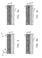
- the layered heater 10 comprises a number of layers disposed on a substrate 12, wherein the substrate 12 may be a separate element disposed proximate the part or device to be heated, or the substrate 12 may be the part or device itself.
- the layers preferably comprise a dielectric layer 14, a resistive layer 16, and a protective layer 18.
- the dielectric layer 14 provides electrical isolation between the substrate 12 and the resistive layer 16 and is formed on the substrate 12 in a thickness commensurate with the power output, applied voltage, intended application temperature, or combinations thereof, of the layered heater 10.
- the resistive layer 16 is formed on the dielectric layer 14 and provides a heater circuit for the layered heater 10, thereby providing the heat to the substrate 12.
- the protective layer 18 is formed on the resistive layer 16 and is preferably an insulator, however other materials such as an electrically or thermally conductive material may also be employed according to the requirements of a specific heating application while remaining within the scope of the present invention.
- the layered heater 10 is shown in a generally cylindrical configuration with a spiral resistive circuit, however, other configurations and circuit patterns may also be employed while remaining within the scope of the present invention.
- terminal pads 20 are preferably disposed on the dielectric layer 14 and are in contact with the resistive layer 16. Accordingly, electrical leads 22 are in contact with the terminal pads 20 and connect the resistive layer 16 to a power source (not shown). (Only one terminal pad 20 and one electrical lead 22 are shown for clarity, and it should be understood that two terminal pads 20 with one electrical lead 22 per terminal pad 20 is the preferred form of the present invention).
- the terminal pads 20 are not required to be in contact with the dielectric layer 14 and thus the illustration of the embodiment in Figure 1 is not intended to limit the scope of the present invention, so long as the terminal pads 20 are electrically connected to the resistive layer 16 in some form.
- the protective layer 18 is disposed over the resistive layer 16 and is preferably a dielectric material for electrical isolation and protection of the resistive layer 16 from the operating environment. Additionally, the protective layer 18 may cover a portion of the terminal pads so long as there remains sufficient area to promote an electrical connection with the power source.
- the individual layers of the layered heater 10 are formed by different layered processes in order to take advantage of the benefits of each process for an overall synergistic result.
- the dielectric layer 14 is formed by a thermal spraying process and the resistive layer 16 is formed by a thick film process.
- a thermal spraying process for the dielectric layer 14 an increased number of materials can be used as the substrate 12 that would otherwise be incompatible with thick film application of the dielectric layer 14.
- a 304 stainless steel for a high temperature application can be used as a substrate 12, which cannot be used with a thick film process due to the excessive coefficient of thermal expansion (CTE) mismatch between this alloy and the possible thick film dielectric glasses.
- CTE coefficient of thermal expansion
- the CTE characteristics and insulation resistance property of thick film glasses is inversely proportional.
- Other compatibility issues may arise with substrates having a low temperature capability, e.g., plastics, and also with a substrate that comprises a heat treated surface or other property that could be adversely affected by the high temperature firing process associated with thick films.
- Additional substrate 12 materials may include, but are not limited to, nickel-plated copper, aluminum, stainless steel, mild steels, tool steels, refractory alloys, aluminum oxide, and aluminum nitride.
- the resistive layer 16 is preferably formed on the dielectric layer 14 using a film printing head in one form of the present invention. Fabrication of the layers using this thick film process is shown and described in U.S. Patent No. 5,973,296 , which is commonly assigned with the present application and the contents of which are incorporated herein by reference in their entirety.
- Additional thick film processes may include, by way of example, screen printing, spraying, rolling, and transfer printing, among others.
- the terminal pads 20 are also preferably formed using a thick film process in one form of the present invention.
- the protective layer 18 is formed using a thermal spraying process. Therefore, the preferred form of the present invention includes a thermal sprayed dielectric layer 14, a thick film resistive layer 16 and terminal pads 20, and a thermal sprayed protective layer 18.
- this form of the present invention has the added advantage of requiring only a single firing sequence to cure the resistive layer 16 and the terminal pads 20 rather than multiple firing sequences that would be required if all of the layers were formed using a thick film layered process. With only a single firing sequence, the selection of resistor materials is greatly expanded.
- a typical thick film resistor layer must be able to withstand the temperatures of the firing sequence of the protective layer, which will often dictate a higher firing temperature resistor.
- the interface stresses between the high expansion substrate and the lower expansion dielectric layer will be reduced, thus promoting a more reliable system.
- the layered heater 10 has broader applicability and is manufactured more efficiently according to the teachings of the present invention.
- a number of combinations of layered processes may be used for each individual layer according to specific heater requirements.
- the processes for each layer as shown in Table I should not be construed as limiting the scope of the present invention, and the teachings of the present invention are that of different layered processes for different functional layers within the layered heater 10.
- a first layered process is employed for a first layer (e.g., thermal spraying for the dielectric layer 14), and a second layered process is employed for a second layer (e.g., thick film for the resistive layer 16) in accordance with the principles of the present invention.
- the thermal spraying processes may include, by way of example, flame spraying, plasma spraying, wire arc spraying, and HVOF (High Velocity Oxygen Fuel), among others.
- the thick film processes may also include, by way of example, screen printing, spraying, rolling, and transfer printing, among others.
- the thin film processes may include ion plating, sputtering, chemical vapor deposition (CVD), and physical vapor deposition (PVD), among others. Thin film processes such as those disclosed in U.S. Patent Nos.
- the layers are formed using sol-gel materials.
- the sol-gel layers are formed using processes such as dipping, spinning, or painting, among others.
- layered heater should be construed to include heaters that comprise functional layers (e.g., dielectric layer 14, resistive layer 16, and protective layer 18, among others as described in greater detail below), wherein each layer is formed through application or accumulation of a material to a substrate or another layer using processes associated with thick film, thin film, thermal spraying, or sol-gel, among others. These processes are also referred to as “layered processes,” “layering processes,” or “layered heater processes.”
- an additional functional layer between the substrate 12 and the dielectric layer 14 may be beneficial or even required when using thermal spraying processes for the dielectric layer 14.
- This layer is referred to as a bond layer 30 and functions to promote adhesion of the thermally sprayed dielectric layer 14 to the substrate 12.
- the bond layer 30 is preferably formed on the substrate 12 using a layered process such as wire arc spraying and is preferably a material such as a nickel-aluminum alloy.
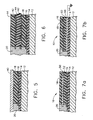
- yet another functional layer may be employed between the substrate 12 and the dielectric layer 14.
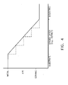
- This layer is referred to as a graded layer 32 and is used to provide a CTE transition between the substrate 12 and the dielectric layer 14 when the difference in CTEs between these layers is relatively large.
- the graded layer 32 provides a transition in CTE as illustrated in Figure 4 , which may be linear/continuous or step-changed as shown by the solid and dashed traces, respectively, or another function as required by specific application requirements.
- the material for the graded layer 32 is preferably a ceramic, a material consisting of a blend of ceramic and metal powders, however, other materials may also be employed.
- both a bond layer 30 and a graded layer 32 as previously described may be employed in another form.
- the bond layer 30 is formed on the substrate 12, and the graded layer 32 is formed on the bond layer 30, wherein the bond layer 30 is used to promote an improved adhesion characteristic between the substrate 12 and the graded layer 32.
- the dielectric layer 14 is formed on the graded layer 32 and thus the graded layer 32 provides a transition in CTE from the substrate 12 to the dielectric layer 14.
- the layered heater 10 may also employ an additional functional layer that is formed on the protective layer 18, namely, an overcoat layer 40.
- the overcoat layer 40 is preferably formed using a layered process and may include by way of example a machinable metal layer, a non-stick coating layer, an emissivity modifier layer, a thermal insulator layer, a visible performance layer, (e.g., temperature sensitive material that indicates temperature via color), or a durability enhancer layer, among others.
- These functional layers may also include additional resistive layers as shown in Figure 6 , wherein a plurality of resistive layers 42 are formed on construed as limiting the scope of the present Additional functional layers, further, in different locations throughout the corresponding plurality of dielectric layers 44.
- the plurality of resistive layers 42 may be required for additional heater output in the form of wattage or may also be used for redundancy of the layered heater 10, for example in the event that the resistive layer 16 fails.
- the plurality of resistive layers 42 may also be employed to satisfy resistance requirements for applications where high or low resistance is required in a small effective heated area, or over a limited footprint. Additionally, multiple circuits, or resistive layer patterns, may be employed within the same resistive layer, or among several layers.
- each of the resistive layers 42 may have different patterns or may be electrically tied to alternate power terminals. Accordingly, the configuration of the plurality of resistive layers 42 as illustrated should not be construed as limiting the scope of the present invention.
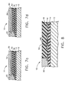
- Additional forms of functional layers are illustrated in Figures 7a-7d , which are intended to be exemplary and not to limit the possible functional layers for the layered heater 10.
- the additional functional layer is a sensor layer 50.
- the sensor layer 50 is preferably a Resistance Temperature Detector (RTD) temperature sensor and is formed on a dielectric layer 52 using a thin film process, although other processes may be employed.
- RTD Resistance Temperature Detector
- FIG. 7b illustrates a layered heater 10 having a functional layer of a ground shield 60, which is employed to isolate and drain any leakage current to and/or from the layered heater 10.
- the ground shield 60 is formed between dielectric layers 14 and 62 and is connected to an independent terminal for appropriate are incorporated herein by reference in their entirety. Such variations are not to be regarded as a departure from the spirit and scope of the invention as defined in the claims.
Landscapes
- Resistance Heating (AREA)
- Surface Heating Bodies (AREA)
Applications Claiming Priority (2)
| Application Number | Priority Date | Filing Date | Title |
|---|---|---|---|
| US10/752,359 US8680443B2 (en) | 2004-01-06 | 2004-01-06 | Combined material layering technologies for electric heaters |
| EP05705126.0A EP1702499B2 (fr) | 2004-01-06 | 2005-01-05 | Techniques d'empilement de materiaux combines pour dispositifs de chauffage electriques |
Related Parent Applications (3)
| Application Number | Title | Priority Date | Filing Date |
|---|---|---|---|
| EP05705126.0A Division EP1702499B2 (fr) | 2004-01-06 | 2005-01-05 | Techniques d'empilement de materiaux combines pour dispositifs de chauffage electriques |
| EP05705126.0A Division-Into EP1702499B2 (fr) | 2004-01-06 | 2005-01-05 | Techniques d'empilement de materiaux combines pour dispositifs de chauffage electriques |
| EP05705126.0 Division | 2005-01-05 |
Publications (3)
| Publication Number | Publication Date |
|---|---|
| EP2134142A2 true EP2134142A2 (fr) | 2009-12-16 |
| EP2134142A3 EP2134142A3 (fr) | 2012-03-14 |
| EP2134142B1 EP2134142B1 (fr) | 2015-03-11 |
Family
ID=34711614
Family Applications (2)
| Application Number | Title | Priority Date | Filing Date |
|---|---|---|---|
| EP09010198.1A Expired - Lifetime EP2134142B1 (fr) | 2004-01-06 | 2005-01-05 | Technologies de mise en couches de matériel combiné pour des chauffages électriques |
| EP05705126.0A Expired - Lifetime EP1702499B2 (fr) | 2004-01-06 | 2005-01-05 | Techniques d'empilement de materiaux combines pour dispositifs de chauffage electriques |
Family Applications After (1)
| Application Number | Title | Priority Date | Filing Date |
|---|---|---|---|
| EP05705126.0A Expired - Lifetime EP1702499B2 (fr) | 2004-01-06 | 2005-01-05 | Techniques d'empilement de materiaux combines pour dispositifs de chauffage electriques |
Country Status (6)
| Country | Link |
|---|---|
| US (2) | US8680443B2 (fr) |
| EP (2) | EP2134142B1 (fr) |
| CN (1) | CN1918945B (fr) |
| CA (1) | CA2552559C (fr) |
| TW (1) | TWI301996B (fr) |
| WO (1) | WO2005069689A2 (fr) |
Families Citing this family (74)
| Publication number | Priority date | Publication date | Assignee | Title |
|---|---|---|---|---|
| US7193180B2 (en) * | 2003-05-21 | 2007-03-20 | Lexmark International, Inc. | Resistive heater comprising first and second resistive traces, a fuser subassembly including such a resistive heater and a universal heating apparatus including first and second resistive traces |
| US7196295B2 (en) * | 2003-11-21 | 2007-03-27 | Watlow Electric Manufacturing Company | Two-wire layered heater system |
| DE102004033251B3 (de) * | 2004-07-08 | 2006-03-09 | Vishay Bccomponents Beyschlag Gmbh | Schmelzsicherung für einem Chip |
| US8536496B2 (en) * | 2004-09-15 | 2013-09-17 | Watlow Electric Manufacturing Company | Adaptable layered heater system |
| EP1803328B1 (fr) * | 2004-09-30 | 2012-04-11 | Watlow Electric Manufacturing Company | Systeme de chauffage modulaire en couches |
| US7280750B2 (en) * | 2005-10-17 | 2007-10-09 | Watlow Electric Manufacturing Company | Hot runner nozzle heater and methods of manufacture thereof |
| US8384504B2 (en) * | 2006-01-06 | 2013-02-26 | Quantum Design International, Inc. | Superconducting quick switch |
| NL2000081C2 (nl) * | 2006-05-23 | 2007-11-26 | Ferro Techniek Holding Bv | Elektrische verwarmingsinrichting met temperatuurdetectie door dielektrische laag. |
| EP2044810B1 (fr) * | 2006-07-20 | 2012-06-13 | Watlow Electric Manufacturing Company | Système chauffant multicouche à revêtements conducteurs |
| US7572480B2 (en) * | 2006-10-19 | 2009-08-11 | Federal-Mogul World Wide, Inc. | Method of fabricating a multilayer ceramic heating element |
| US8134434B2 (en) * | 2007-01-05 | 2012-03-13 | Quantum Design, Inc. | Superconducting quick switch |
| GB2446412A (en) * | 2007-02-09 | 2008-08-13 | Duna Entpr Sa | Heating structure for hair dryers |
| AU2008219092A1 (en) * | 2007-02-20 | 2008-08-28 | Thermoceramix Inc. | Gas heating apparatus and methods |
| NL2000685C2 (nl) * | 2007-06-06 | 2008-12-09 | Ferro Techniek Holding Bv | Verwarmingselement en vloeistofhouder voorzien van een dergelijk verwarmingselement. |
| US8557082B2 (en) | 2007-07-18 | 2013-10-15 | Watlow Electric Manufacturing Company | Reduced cycle time manufacturing processes for thick film resistive devices |
| US8089337B2 (en) * | 2007-07-18 | 2012-01-03 | Watlow Electric Manufacturing Company | Thick film layered resistive device employing a dielectric tape |
| JP5238038B2 (ja) * | 2007-11-16 | 2013-07-17 | ワトロウ エレクトリック マニュファクチュアリング カンパニー | 防湿性積層スリーブ加熱器とその製造方法 |
| US10135021B2 (en) * | 2008-02-29 | 2018-11-20 | Corning Incorporated | Frit sealing using direct resistive heating |
| ATE542393T1 (de) * | 2008-03-18 | 2012-02-15 | Watlow Electric Mfg | Geschichtetes heizsystem mit wabenkernstruktur |
| US8061402B2 (en) * | 2008-04-07 | 2011-11-22 | Watlow Electric Manufacturing Company | Method and apparatus for positioning layers within a layered heater system |
| CN102067719B (zh) * | 2008-04-22 | 2014-07-16 | 达泰克涂料股份公司 | 厚膜高温热塑性绝缘加热元件 |
| US8306408B2 (en) * | 2008-05-30 | 2012-11-06 | Thermoceramix Inc. | Radiant heating using heater coatings |
| US20110188838A1 (en) * | 2008-05-30 | 2011-08-04 | Thermoceramix, Inc. | Radiant heating using heater coatings |
| NL2001690C2 (en) * | 2008-06-16 | 2009-12-17 | Otter Controls Ltd | Device and method for generating steam, and heating element for use in such a device. |
| EP2310681A4 (fr) * | 2008-07-01 | 2017-04-12 | Brooks Automation, Inc. | Procédé et appareil de régulation thermique d'une pompe cryostatique |
| WO2010054128A2 (fr) | 2008-11-05 | 2010-05-14 | Red E Innovations, Llc | Coffre-fort de données, système et procédé |
| TWI477252B (zh) * | 2009-11-03 | 2015-03-21 | Ind Tech Res Inst | 加熱保溫承載器 |
| GB2477338B (en) * | 2010-01-29 | 2011-12-07 | Gkn Aerospace Services Ltd | Electrothermal heater |
| US8978450B2 (en) * | 2010-07-22 | 2015-03-17 | Watlow Electric Manufacturing Company | Combination fluid sensor system |
| US9417572B2 (en) | 2010-12-17 | 2016-08-16 | Lexmark International, Inc. | Fuser heating element for an electrophotographic imaging device |
| US10025244B2 (en) | 2010-12-17 | 2018-07-17 | Lexmark International, Inc. | Circuit and method for a hybrid heater with dual function heating capability |
| US9668302B2 (en) * | 2011-03-31 | 2017-05-30 | Kyocera Corporation | Ceramic heater |
| AU2012301903B2 (en) | 2011-08-30 | 2015-07-09 | Watlow Electric Manufacturing Company | High definition heater system having a fluid medium |
| AU2015203558B2 (en) * | 2011-08-30 | 2017-04-13 | Watlow Electric Manufacturing Company | High definition heater and method of operation |
| US20130071716A1 (en) * | 2011-09-16 | 2013-03-21 | General Electric Company | Thermal management device |
| DE102012103120B4 (de) * | 2012-04-11 | 2025-04-30 | Günther Heisskanaltechnik Gmbh | Werkzeugeinsatz mit Schichtheizung, Formplatte mit einem solchen Werkzeugeinsatz und Verfahren zum Betrieb eines solchen Werkzeugeinsatzes |
| US9224626B2 (en) * | 2012-07-03 | 2015-12-29 | Watlow Electric Manufacturing Company | Composite substrate for layered heaters |
| US20150016083A1 (en) * | 2013-07-05 | 2015-01-15 | Stephen P. Nootens | Thermocompression bonding apparatus and method |
| CN103376507B (zh) * | 2013-07-24 | 2015-01-14 | 大豪信息技术(威海)有限公司 | 光纤熔接机用高效加热槽及光纤熔接机 |
| DE102013216668A1 (de) * | 2013-08-22 | 2015-02-26 | Continental Automotive Gmbh | Verfahren und Vorrichtung zum Herstellen einer Heizwicklung auf einen metallischen Grundkörper |
| US9518946B2 (en) | 2013-12-04 | 2016-12-13 | Watlow Electric Manufacturing Company | Thermographic inspection system |
| JP6219227B2 (ja) | 2014-05-12 | 2017-10-25 | 東京エレクトロン株式会社 | ヒータ給電機構及びステージの温度制御方法 |
| CN111422238B (zh) * | 2014-06-02 | 2022-10-25 | Tk控股公司 | 用于在方向盘的传感器垫上印刷传感器电路的系统和方法 |
| US9818512B2 (en) * | 2014-12-08 | 2017-11-14 | Vishay Dale Electronics, Llc | Thermally sprayed thin film resistor and method of making |
| JP6256454B2 (ja) * | 2015-11-30 | 2018-01-10 | 株式会社デンソー | ヒータプレート、このヒータプレートを用いる熱流束センサの製造装置、このヒータプレートの製造方法、及び、このヒータプレートの製造装置 |
| GB2545396B (en) * | 2015-12-07 | 2021-10-06 | Kenwood Ltd | Heater cassette |
| US10690414B2 (en) | 2015-12-11 | 2020-06-23 | Lam Research Corporation | Multi-plane heater for semiconductor substrate support |
| US10557584B2 (en) | 2015-12-16 | 2020-02-11 | Watlow Electric Manufacturing Company | Modular heater systems |
| JP6657998B2 (ja) * | 2016-01-26 | 2020-03-04 | 富士ゼロックス株式会社 | 定着装置、画像形成装置及び加熱装置 |
| US10340171B2 (en) | 2016-05-18 | 2019-07-02 | Lam Research Corporation | Permanent secondary erosion containment for electrostatic chuck bonds |
| US11069553B2 (en) * | 2016-07-07 | 2021-07-20 | Lam Research Corporation | Electrostatic chuck with features for preventing electrical arcing and light-up and improving process uniformity |
| CN106982480B (zh) * | 2016-08-30 | 2021-02-26 | 广东天物新材料科技有限公司 | 一种多层厚膜发热元件 |
| CN106637043A (zh) * | 2016-11-23 | 2017-05-10 | 东莞珂洛赫慕电子材料科技有限公司 | 一种等离子喷涂不锈钢管电热器件 |
| CN106676457A (zh) * | 2016-11-23 | 2017-05-17 | 东莞珂洛赫慕电子材料科技有限公司 | 一种等离子喷涂电热器件介质层的制备方法 |
| CN106555152A (zh) * | 2016-11-23 | 2017-04-05 | 东莞珂洛赫慕电子材料科技有限公司 | 一种等离子喷涂铝基材电热器件电阻层的制备方法 |
| CN106555151A (zh) * | 2016-11-23 | 2017-04-05 | 东莞珂洛赫慕电子材料科技有限公司 | 一种等离子喷涂铝基材电热器件及其制备方法 |
| CN106793205A (zh) * | 2016-12-05 | 2017-05-31 | 东莞佐佑电子科技有限公司 | 一种厚膜发热管防局部干烧结构及其方法 |
| US10910195B2 (en) | 2017-01-05 | 2021-02-02 | Lam Research Corporation | Substrate support with improved process uniformity |
| GB2562075B (en) | 2017-05-03 | 2022-03-16 | Jemella Ltd | Barrel for hair styling appliance |
| TWI815813B (zh) * | 2017-08-04 | 2023-09-21 | 荷蘭商Asm智慧財產控股公司 | 用於分配反應腔內氣體的噴頭總成 |
| US10761041B2 (en) | 2017-11-21 | 2020-09-01 | Watlow Electric Manufacturing Company | Multi-parallel sensor array system |
| WO2019199506A1 (fr) | 2018-04-11 | 2019-10-17 | Watlow Electric Manufacturing Company | Dispositif de chauffage résistif avec broches d'alimentation à détection de température et jonction de détection auxiliaire |
| MX2021002964A (es) | 2018-09-14 | 2021-05-12 | Watlow Electric Mfg | Sistema y metodo para un control de horneado en circuito cerrado. |
| US11562890B2 (en) * | 2018-12-06 | 2023-01-24 | Applied Materials, Inc. | Corrosion resistant ground shield of processing chamber |
| US11240881B2 (en) | 2019-04-08 | 2022-02-01 | Watlow Electric Manufacturing Company | Method of manufacturing and adjusting a resistive heater |
| TWI809369B (zh) | 2020-04-06 | 2023-07-21 | 美商瓦特洛威電子製造公司 | 具備可互換式輔助感測接合部之模組化加熱器總成 |
| US11730205B2 (en) | 2020-10-20 | 2023-08-22 | Dr. Dabber Inc. | Quick connect adapter and electronic vaporizer having a ceramic heating element having a quick connect adapter |
| US11064738B2 (en) * | 2020-10-20 | 2021-07-20 | Dr. Dabber Inc. | Ceramic heating element with embedded temperature sensor and electronic vaporizer having a ceramic heating element with embedded temperature sensor |
| EP4349132A4 (fr) * | 2021-06-01 | 2025-02-19 | BorgWarner Inc. | Dispositif de chauffage et procédé de production d'un dispositif de chauffage |
| GB2618803A (en) * | 2022-05-17 | 2023-11-22 | Dyson Technology Ltd | Thick film heating elements |
| US11828796B1 (en) | 2023-05-02 | 2023-11-28 | AEM Holdings Ltd. | Integrated heater and temperature measurement |
| US12013432B1 (en) | 2023-08-23 | 2024-06-18 | Aem Singapore Pte. Ltd. | Thermal control wafer with integrated heating-sensing elements |
| US12085609B1 (en) | 2023-08-23 | 2024-09-10 | Aem Singapore Pte. Ltd. | Thermal control wafer with integrated heating-sensing elements |
| US12000885B1 (en) | 2023-12-20 | 2024-06-04 | Aem Singapore Pte. Ltd. | Multiplexed thermal control wafer and coldplate |
Citations (2)
| Publication number | Priority date | Publication date | Assignee | Title |
|---|---|---|---|---|
| US5973296A (en) | 1998-10-20 | 1999-10-26 | Watlow Electric Manufacturing Company | Thick film heater for injection mold runner nozzle |
| US6305923B1 (en) | 1998-06-12 | 2001-10-23 | Husky Injection Molding Systems Ltd. | Molding system using film heaters and/or sensors |
Family Cites Families (26)
| Publication number | Priority date | Publication date | Assignee | Title |
|---|---|---|---|---|
| BE522502A (fr) * | 1952-09-02 | |||
| DE965859C (de) | 1952-09-02 | 1957-06-27 | Wmf Wuerttemberg Metallwaren | Verfahren zur Herstellung von elektrisch beheizten Metallgefaessen zum Kochen, Braten oder Backen |
| US3961155A (en) * | 1974-06-24 | 1976-06-01 | Gulton Industries, Inc. | Thermal printing element arrays |
| DE3728466A1 (de) | 1987-08-26 | 1989-03-09 | Ego Elektro Blanc & Fischer | Kochgeraet |
| US4920254A (en) * | 1988-02-22 | 1990-04-24 | Sierracin Corporation | Electrically conductive window and a method for its manufacture |
| KR960005321B1 (ko) | 1990-04-24 | 1996-04-23 | 가부시끼가이샤 히다찌세이사꾸쇼 | 박막저항체를 갖는 전자회로소자 및 그 제조방법 |
| DE4022844C1 (fr) * | 1990-07-18 | 1992-02-27 | Schott Glaswerke, 6500 Mainz, De | |
| US5120936A (en) * | 1990-08-22 | 1992-06-09 | Industrial Technology Research Institute | Multiplex heating system with temperature control |
| WO1995015670A1 (fr) | 1993-11-30 | 1995-06-08 | Alliedsignal Inc. | Dispositif de chauffage composite electriquement conducteur et procede de fabrication de ce dispositif |
| GB9511618D0 (en) * | 1995-06-08 | 1995-08-02 | Deeman Product Dev Limited | Electrical heating elements |
| US6222168B1 (en) * | 1995-10-27 | 2001-04-24 | Medical Indicators, Inc. | Shielding method for microwave heating of infant formulate to a safe and uniform temperature |
| GB9602873D0 (en) * | 1996-02-13 | 1996-04-10 | Dow Corning Sa | Heating elements and process for manufacture thereof |
| EP0853444B1 (fr) † | 1997-01-10 | 2005-11-23 | E.G.O. ELEKTRO-GERÄTEBAU GmbH | Système à cuire avec une plaque de cuisson électrique, transférant la chaleur par conduction |
| WO1998051127A1 (fr) * | 1997-05-06 | 1998-11-12 | Thermoceramix, L.L.C. | Revetements resistants obtenus par formation d'un depot |
| US6127654A (en) * | 1997-08-01 | 2000-10-03 | Alkron Manufacturing Corporation | Method for manufacturing heating element |
| DE69830984T2 (de) | 1998-06-25 | 2006-07-13 | Electrolux Home Care Products Ltd. (N.D.Ges.D.Staates Texas), Cleveland | Dünnschichtheizanordnung |
| DE19906100C2 (de) | 1999-02-13 | 2003-07-31 | Sls Micro Technology Gmbh | Thermischer Durchflußsensor in Mikrosystemtechnik |
| GB2351894B (en) | 1999-05-04 | 2003-10-15 | Otter Controls Ltd | Improvements relating to heating elements |
| US6222166B1 (en) * | 1999-08-09 | 2001-04-24 | Watlow Electric Manufacturing Co. | Aluminum substrate thick film heater |
| US6225608B1 (en) * | 1999-11-30 | 2001-05-01 | White Consolidated Industries, Inc. | Circular film heater |
| GB2359234A (en) * | 1999-12-10 | 2001-08-15 | Jeffery Boardman | Resistive heating elements composed of binary metal oxides, the metals having different valencies |
| US6433319B1 (en) * | 2000-12-15 | 2002-08-13 | Brian A. Bullock | Electrical, thin film termination |
| US6580061B2 (en) * | 2000-02-01 | 2003-06-17 | Trebor International Inc | Durable, non-reactive, resistive-film heater |
| GB2363307A (en) | 2000-06-05 | 2001-12-12 | Otter Controls Ltd | Thick film heating element stack |
| US6817088B1 (en) * | 2000-06-16 | 2004-11-16 | Watlow Electric Msg.C | Termination method for thick film resistance heater |
| DE10110789C1 (de) | 2001-03-06 | 2002-07-04 | Schott Glas | Kochgerät mit einer nicht planaren, mehrdimensional geformten Kochfläche aus Glas- oder Glaskeramik |
-
2004
- 2004-01-06 US US10/752,359 patent/US8680443B2/en active Active
-
2005
- 2005-01-05 WO PCT/US2005/000341 patent/WO2005069689A2/fr not_active Ceased
- 2005-01-05 EP EP09010198.1A patent/EP2134142B1/fr not_active Expired - Lifetime
- 2005-01-05 CA CA2552559A patent/CA2552559C/fr not_active Expired - Fee Related
- 2005-01-05 CN CN2005800050372A patent/CN1918945B/zh not_active Expired - Lifetime
- 2005-01-05 EP EP05705126.0A patent/EP1702499B2/fr not_active Expired - Lifetime
- 2005-01-06 TW TW094100389A patent/TWI301996B/zh not_active IP Right Cessation
-
2006
- 2006-01-12 US US11/330,606 patent/US20060113297A1/en not_active Abandoned
Patent Citations (4)
| Publication number | Priority date | Publication date | Assignee | Title |
|---|---|---|---|---|
| US6305923B1 (en) | 1998-06-12 | 2001-10-23 | Husky Injection Molding Systems Ltd. | Molding system using film heaters and/or sensors |
| US6341954B1 (en) | 1998-06-12 | 2002-01-29 | Husky Injection Molding Systems Ltd. | Molding system using film heaters and/or sensors |
| US6575729B2 (en) | 1998-06-12 | 2003-06-10 | Husky Injection Molding Systems Ltd. | Molding system with integrated film heaters and sensors |
| US5973296A (en) | 1998-10-20 | 1999-10-26 | Watlow Electric Manufacturing Company | Thick film heater for injection mold runner nozzle |
Also Published As
| Publication number | Publication date |
|---|---|
| EP1702499A2 (fr) | 2006-09-20 |
| TWI301996B (en) | 2008-10-11 |
| EP2134142A3 (fr) | 2012-03-14 |
| CN1918945A (zh) | 2007-02-21 |
| WO2005069689A2 (fr) | 2005-07-28 |
| EP1702499B2 (fr) | 2019-11-27 |
| US20050145617A1 (en) | 2005-07-07 |
| CA2552559A1 (fr) | 2005-07-28 |
| US20070278213A2 (en) | 2007-12-06 |
| WO2005069689A3 (fr) | 2005-12-22 |
| US20060113297A1 (en) | 2006-06-01 |
| US8680443B2 (en) | 2014-03-25 |
| EP1702499B1 (fr) | 2016-06-22 |
| CN1918945B (zh) | 2012-10-03 |
| TW200535929A (en) | 2005-11-01 |
| EP2134142B1 (fr) | 2015-03-11 |
| CA2552559C (fr) | 2013-03-12 |
Similar Documents
| Publication | Publication Date | Title |
|---|---|---|
| EP2134142B1 (fr) | Technologies de mise en couches de matériel combiné pour des chauffages électriques | |
| US8536496B2 (en) | Adaptable layered heater system | |
| US8008607B2 (en) | Methods of forming a variable watt density layered heater | |
| US8175446B2 (en) | Hot runner nozzle heater and methods of manufacture thereof | |
| US10159116B2 (en) | Modular layered heater system | |
| CA2719410C (fr) | Appareil de chauffage a manchon stratifie resistant a l'humidite et procede pour sa fabrication | |
| CA2552561C (fr) | Systeme de chauffage en couches a transfert de chaleur adapte | |
| MXPA06007798A (es) | Tecnologia de estratificacion de materiales combinados para calentadores electricos | |
| US20260052606A1 (en) | Monolithic layered heater for thin-walled substrates |
Legal Events
| Date | Code | Title | Description |
|---|---|---|---|
| PUAI | Public reference made under article 153(3) epc to a published international application that has entered the european phase |
Free format text: ORIGINAL CODE: 0009012 |
|
| AC | Divisional application: reference to earlier application |
Ref document number: 1702499 Country of ref document: EP Kind code of ref document: P |
|
| AK | Designated contracting states |
Kind code of ref document: A2 Designated state(s): AT BE BG CH CY CZ DE DK EE ES FI FR GB GR HU IE IS IT LI LT LU MC NL PL PT RO SE SI SK TR |
|
| PUAL | Search report despatched |
Free format text: ORIGINAL CODE: 0009013 |
|
| AK | Designated contracting states |
Kind code of ref document: A3 Designated state(s): AT BE BG CH CY CZ DE DK EE ES FI FR GB GR HU IE IS IT LI LT LU MC NL PL PT RO SE SI SK TR |
|
| RIC1 | Information provided on ipc code assigned before grant |
Ipc: H05B 3/28 20060101AFI20120207BHEP |
|
| RIN1 | Information on inventor provided before grant (corrected) |
Inventor name: STEINHAUSER, LOUIS Inventor name: MCMILLIN, JAMES Inventor name: PTASIENSKI, KEVIN |
|
| 17P | Request for examination filed |
Effective date: 20120804 |
|
| 17Q | First examination report despatched |
Effective date: 20130916 |
|
| GRAP | Despatch of communication of intention to grant a patent |
Free format text: ORIGINAL CODE: EPIDOSNIGR1 |
|
| INTG | Intention to grant announced |
Effective date: 20140624 |
|
| GRAS | Grant fee paid |
Free format text: ORIGINAL CODE: EPIDOSNIGR3 |
|
| GRAP | Despatch of communication of intention to grant a patent |
Free format text: ORIGINAL CODE: EPIDOSNIGR1 |
|
| INTG | Intention to grant announced |
Effective date: 20150105 |
|
| GRAA | (expected) grant |
Free format text: ORIGINAL CODE: 0009210 |
|
| AC | Divisional application: reference to earlier application |
Ref document number: 1702499 Country of ref document: EP Kind code of ref document: P |
|
| AK | Designated contracting states |
Kind code of ref document: B1 Designated state(s): AT BE BG CH CY CZ DE DK EE ES FI FR GB GR HU IE IS IT LI LT LU MC NL PL PT RO SE SI SK TR |
|
| REG | Reference to a national code |
Ref country code: GB Ref legal event code: FG4D |
|
| REG | Reference to a national code |
Ref country code: CH Ref legal event code: EP |
|
| REG | Reference to a national code |
Ref country code: IE Ref legal event code: FG4D |
|
| REG | Reference to a national code |
Ref country code: AT Ref legal event code: REF Ref document number: 715915 Country of ref document: AT Kind code of ref document: T Effective date: 20150415 |
|
| REG | Reference to a national code |
Ref country code: DE Ref legal event code: R096 Ref document number: 602005046051 Country of ref document: DE Effective date: 20150423 |
|
| REG | Reference to a national code |
Ref country code: NL Ref legal event code: T3 |
|
| PG25 | Lapsed in a contracting state [announced via postgrant information from national office to epo] |
Ref country code: SE Free format text: LAPSE BECAUSE OF FAILURE TO SUBMIT A TRANSLATION OF THE DESCRIPTION OR TO PAY THE FEE WITHIN THE PRESCRIBED TIME-LIMIT Effective date: 20150311 Ref country code: ES Free format text: LAPSE BECAUSE OF FAILURE TO SUBMIT A TRANSLATION OF THE DESCRIPTION OR TO PAY THE FEE WITHIN THE PRESCRIBED TIME-LIMIT Effective date: 20150311 Ref country code: FI Free format text: LAPSE BECAUSE OF FAILURE TO SUBMIT A TRANSLATION OF THE DESCRIPTION OR TO PAY THE FEE WITHIN THE PRESCRIBED TIME-LIMIT Effective date: 20150311 Ref country code: LT Free format text: LAPSE BECAUSE OF FAILURE TO SUBMIT A TRANSLATION OF THE DESCRIPTION OR TO PAY THE FEE WITHIN THE PRESCRIBED TIME-LIMIT Effective date: 20150311 |
|
| REG | Reference to a national code |
Ref country code: LT Ref legal event code: MG4D |
|
| PG25 | Lapsed in a contracting state [announced via postgrant information from national office to epo] |
Ref country code: GR Free format text: LAPSE BECAUSE OF FAILURE TO SUBMIT A TRANSLATION OF THE DESCRIPTION OR TO PAY THE FEE WITHIN THE PRESCRIBED TIME-LIMIT Effective date: 20150612 |
|
| PG25 | Lapsed in a contracting state [announced via postgrant information from national office to epo] |
Ref country code: EE Free format text: LAPSE BECAUSE OF FAILURE TO SUBMIT A TRANSLATION OF THE DESCRIPTION OR TO PAY THE FEE WITHIN THE PRESCRIBED TIME-LIMIT Effective date: 20150311 Ref country code: PT Free format text: LAPSE BECAUSE OF FAILURE TO SUBMIT A TRANSLATION OF THE DESCRIPTION OR TO PAY THE FEE WITHIN THE PRESCRIBED TIME-LIMIT Effective date: 20150713 Ref country code: SK Free format text: LAPSE BECAUSE OF FAILURE TO SUBMIT A TRANSLATION OF THE DESCRIPTION OR TO PAY THE FEE WITHIN THE PRESCRIBED TIME-LIMIT Effective date: 20150311 Ref country code: CZ Free format text: LAPSE BECAUSE OF FAILURE TO SUBMIT A TRANSLATION OF THE DESCRIPTION OR TO PAY THE FEE WITHIN THE PRESCRIBED TIME-LIMIT Effective date: 20150311 Ref country code: RO Free format text: LAPSE BECAUSE OF FAILURE TO SUBMIT A TRANSLATION OF THE DESCRIPTION OR TO PAY THE FEE WITHIN THE PRESCRIBED TIME-LIMIT Effective date: 20150311 |
|
| PG25 | Lapsed in a contracting state [announced via postgrant information from national office to epo] |
Ref country code: PL Free format text: LAPSE BECAUSE OF FAILURE TO SUBMIT A TRANSLATION OF THE DESCRIPTION OR TO PAY THE FEE WITHIN THE PRESCRIBED TIME-LIMIT Effective date: 20150311 Ref country code: IS Free format text: LAPSE BECAUSE OF FAILURE TO SUBMIT A TRANSLATION OF THE DESCRIPTION OR TO PAY THE FEE WITHIN THE PRESCRIBED TIME-LIMIT Effective date: 20150711 |
|
| REG | Reference to a national code |
Ref country code: DE Ref legal event code: R097 Ref document number: 602005046051 Country of ref document: DE |
|
| PG25 | Lapsed in a contracting state [announced via postgrant information from national office to epo] |
Ref country code: IT Free format text: LAPSE BECAUSE OF FAILURE TO SUBMIT A TRANSLATION OF THE DESCRIPTION OR TO PAY THE FEE WITHIN THE PRESCRIBED TIME-LIMIT Effective date: 20150311 |
|
| PLBE | No opposition filed within time limit |
Free format text: ORIGINAL CODE: 0009261 |
|
| STAA | Information on the status of an ep patent application or granted ep patent |
Free format text: STATUS: NO OPPOSITION FILED WITHIN TIME LIMIT |
|
| PG25 | Lapsed in a contracting state [announced via postgrant information from national office to epo] |
Ref country code: DK Free format text: LAPSE BECAUSE OF FAILURE TO SUBMIT A TRANSLATION OF THE DESCRIPTION OR TO PAY THE FEE WITHIN THE PRESCRIBED TIME-LIMIT Effective date: 20150311 |
|
| 26N | No opposition filed |
Effective date: 20151214 |
|
| PG25 | Lapsed in a contracting state [announced via postgrant information from national office to epo] |
Ref country code: SI Free format text: LAPSE BECAUSE OF FAILURE TO SUBMIT A TRANSLATION OF THE DESCRIPTION OR TO PAY THE FEE WITHIN THE PRESCRIBED TIME-LIMIT Effective date: 20150311 |
|
| PG25 | Lapsed in a contracting state [announced via postgrant information from national office to epo] |
Ref country code: BE Free format text: LAPSE BECAUSE OF NON-PAYMENT OF DUE FEES Effective date: 20160131 |
|
| PG25 | Lapsed in a contracting state [announced via postgrant information from national office to epo] |
Ref country code: BE Free format text: LAPSE BECAUSE OF FAILURE TO SUBMIT A TRANSLATION OF THE DESCRIPTION OR TO PAY THE FEE WITHIN THE PRESCRIBED TIME-LIMIT Effective date: 20150311 Ref country code: LU Free format text: LAPSE BECAUSE OF FAILURE TO SUBMIT A TRANSLATION OF THE DESCRIPTION OR TO PAY THE FEE WITHIN THE PRESCRIBED TIME-LIMIT Effective date: 20160105 |
|
| REG | Reference to a national code |
Ref country code: CH Ref legal event code: PL |
|
| PG25 | Lapsed in a contracting state [announced via postgrant information from national office to epo] |
Ref country code: MC Free format text: LAPSE BECAUSE OF FAILURE TO SUBMIT A TRANSLATION OF THE DESCRIPTION OR TO PAY THE FEE WITHIN THE PRESCRIBED TIME-LIMIT Effective date: 20150311 |
|
| REG | Reference to a national code |
Ref country code: AT Ref legal event code: UEP Ref document number: 715915 Country of ref document: AT Kind code of ref document: T Effective date: 20150311 |
|
| REG | Reference to a national code |
Ref country code: FR Ref legal event code: ST Effective date: 20160930 |
|
| PG25 | Lapsed in a contracting state [announced via postgrant information from national office to epo] |
Ref country code: CH Free format text: LAPSE BECAUSE OF NON-PAYMENT OF DUE FEES Effective date: 20160131 Ref country code: LI Free format text: LAPSE BECAUSE OF NON-PAYMENT OF DUE FEES Effective date: 20160131 |
|
| REG | Reference to a national code |
Ref country code: IE Ref legal event code: MM4A |
|
| PG25 | Lapsed in a contracting state [announced via postgrant information from national office to epo] |
Ref country code: FR Free format text: LAPSE BECAUSE OF NON-PAYMENT OF DUE FEES Effective date: 20160201 |
|
| PG25 | Lapsed in a contracting state [announced via postgrant information from national office to epo] |
Ref country code: IE Free format text: LAPSE BECAUSE OF NON-PAYMENT OF DUE FEES Effective date: 20160105 |
|
| PG25 | Lapsed in a contracting state [announced via postgrant information from national office to epo] |
Ref country code: CY Free format text: LAPSE BECAUSE OF FAILURE TO SUBMIT A TRANSLATION OF THE DESCRIPTION OR TO PAY THE FEE WITHIN THE PRESCRIBED TIME-LIMIT Effective date: 20150311 Ref country code: HU Free format text: LAPSE BECAUSE OF FAILURE TO SUBMIT A TRANSLATION OF THE DESCRIPTION OR TO PAY THE FEE WITHIN THE PRESCRIBED TIME-LIMIT; INVALID AB INITIO Effective date: 20050105 |
|
| PG25 | Lapsed in a contracting state [announced via postgrant information from national office to epo] |
Ref country code: TR Free format text: LAPSE BECAUSE OF FAILURE TO SUBMIT A TRANSLATION OF THE DESCRIPTION OR TO PAY THE FEE WITHIN THE PRESCRIBED TIME-LIMIT Effective date: 20150311 |
|
| PG25 | Lapsed in a contracting state [announced via postgrant information from national office to epo] |
Ref country code: BG Free format text: LAPSE BECAUSE OF FAILURE TO SUBMIT A TRANSLATION OF THE DESCRIPTION OR TO PAY THE FEE WITHIN THE PRESCRIBED TIME-LIMIT Effective date: 20150311 |
|
| PGFP | Annual fee paid to national office [announced via postgrant information from national office to epo] |
Ref country code: AT Payment date: 20181219 Year of fee payment: 15 |
|
| REG | Reference to a national code |
Ref country code: AT Ref legal event code: MM01 Ref document number: 715915 Country of ref document: AT Kind code of ref document: T Effective date: 20200105 |
|
| PG25 | Lapsed in a contracting state [announced via postgrant information from national office to epo] |
Ref country code: AT Free format text: LAPSE BECAUSE OF NON-PAYMENT OF DUE FEES Effective date: 20200105 |
|
| PGFP | Annual fee paid to national office [announced via postgrant information from national office to epo] |
Ref country code: NL Payment date: 20240126 Year of fee payment: 20 |
|
| PGFP | Annual fee paid to national office [announced via postgrant information from national office to epo] |
Ref country code: DE Payment date: 20240129 Year of fee payment: 20 Ref country code: GB Payment date: 20240129 Year of fee payment: 20 |
|
| REG | Reference to a national code |
Ref country code: DE Ref legal event code: R071 Ref document number: 602005046051 Country of ref document: DE |
|
| REG | Reference to a national code |
Ref country code: NL Ref legal event code: MK Effective date: 20250104 |
|
| REG | Reference to a national code |
Ref country code: GB Ref legal event code: PE20 Expiry date: 20250104 |
|
| PG25 | Lapsed in a contracting state [announced via postgrant information from national office to epo] |
Ref country code: GB Free format text: LAPSE BECAUSE OF EXPIRATION OF PROTECTION Effective date: 20250104 |