EP2135304B1 - Diodes électroluminescentes verticales - Google Patents
Diodes électroluminescentes verticales Download PDFInfo
- Publication number
- EP2135304B1 EP2135304B1 EP08718588.0A EP08718588A EP2135304B1 EP 2135304 B1 EP2135304 B1 EP 2135304B1 EP 08718588 A EP08718588 A EP 08718588A EP 2135304 B1 EP2135304 B1 EP 2135304B1
- Authority
- EP
- European Patent Office
- Prior art keywords
- light emitting
- layer
- stack
- semiconductor layer
- multilayer reflector
- Prior art date
- Legal status (The legal status is an assumption and is not a legal conclusion. Google has not performed a legal analysis and makes no representation as to the accuracy of the status listed.)
- Active
Links
Images




Classifications
-
- H—ELECTRICITY
- H10—SEMICONDUCTOR DEVICES; ELECTRIC SOLID-STATE DEVICES NOT OTHERWISE PROVIDED FOR
- H10H—INORGANIC LIGHT-EMITTING SEMICONDUCTOR DEVICES HAVING POTENTIAL BARRIERS
- H10H20/00—Individual inorganic light-emitting semiconductor devices having potential barriers, e.g. light-emitting diodes [LED]
- H10H20/80—Constructional details
- H10H20/862—Resonant cavity structures
-
- H—ELECTRICITY
- H10—SEMICONDUCTOR DEVICES; ELECTRIC SOLID-STATE DEVICES NOT OTHERWISE PROVIDED FOR
- H10H—INORGANIC LIGHT-EMITTING SEMICONDUCTOR DEVICES HAVING POTENTIAL BARRIERS
- H10H20/00—Individual inorganic light-emitting semiconductor devices having potential barriers, e.g. light-emitting diodes [LED]
- H10H20/80—Constructional details
- H10H20/83—Electrodes
- H10H20/832—Electrodes characterised by their material
- H10H20/833—Transparent materials
-
- H—ELECTRICITY
- H10—SEMICONDUCTOR DEVICES; ELECTRIC SOLID-STATE DEVICES NOT OTHERWISE PROVIDED FOR
- H10H—INORGANIC LIGHT-EMITTING SEMICONDUCTOR DEVICES HAVING POTENTIAL BARRIERS
- H10H20/00—Individual inorganic light-emitting semiconductor devices having potential barriers, e.g. light-emitting diodes [LED]
- H10H20/80—Constructional details
- H10H20/83—Electrodes
- H10H20/832—Electrodes characterised by their material
- H10H20/835—Reflective materials
-
- H—ELECTRICITY
- H10—SEMICONDUCTOR DEVICES; ELECTRIC SOLID-STATE DEVICES NOT OTHERWISE PROVIDED FOR
- H10H—INORGANIC LIGHT-EMITTING SEMICONDUCTOR DEVICES HAVING POTENTIAL BARRIERS
- H10H20/00—Individual inorganic light-emitting semiconductor devices having potential barriers, e.g. light-emitting diodes [LED]
- H10H20/80—Constructional details
- H10H20/84—Coatings, e.g. passivation layers or antireflective coatings
- H10H20/841—Reflective coatings, e.g. dielectric Bragg reflectors
-
- H—ELECTRICITY
- H10—SEMICONDUCTOR DEVICES; ELECTRIC SOLID-STATE DEVICES NOT OTHERWISE PROVIDED FOR
- H10H—INORGANIC LIGHT-EMITTING SEMICONDUCTOR DEVICES HAVING POTENTIAL BARRIERS
- H10H20/00—Individual inorganic light-emitting semiconductor devices having potential barriers, e.g. light-emitting diodes [LED]
- H10H20/80—Constructional details
- H10H20/85—Packages
- H10H20/851—Wavelength conversion means
- H10H20/8515—Wavelength conversion means not being in contact with the bodies
-
- H—ELECTRICITY
- H05—ELECTRIC TECHNIQUES NOT OTHERWISE PROVIDED FOR
- H05B—ELECTRIC HEATING; ELECTRIC LIGHT SOURCES NOT OTHERWISE PROVIDED FOR; CIRCUIT ARRANGEMENTS FOR ELECTRIC LIGHT SOURCES, IN GENERAL
- H05B45/00—Circuit arrangements for operating light-emitting diodes [LED]
- H05B45/20—Controlling the colour of the light
-
- H—ELECTRICITY
- H10—SEMICONDUCTOR DEVICES; ELECTRIC SOLID-STATE DEVICES NOT OTHERWISE PROVIDED FOR
- H10H—INORGANIC LIGHT-EMITTING SEMICONDUCTOR DEVICES HAVING POTENTIAL BARRIERS
- H10H20/00—Individual inorganic light-emitting semiconductor devices having potential barriers, e.g. light-emitting diodes [LED]
- H10H20/01—Manufacture or treatment
- H10H20/011—Manufacture or treatment of bodies, e.g. forming semiconductor layers
- H10H20/018—Bonding of wafers
-
- H—ELECTRICITY
- H10—SEMICONDUCTOR DEVICES; ELECTRIC SOLID-STATE DEVICES NOT OTHERWISE PROVIDED FOR
- H10H—INORGANIC LIGHT-EMITTING SEMICONDUCTOR DEVICES HAVING POTENTIAL BARRIERS
- H10H20/00—Individual inorganic light-emitting semiconductor devices having potential barriers, e.g. light-emitting diodes [LED]
- H10H20/80—Constructional details
- H10H20/81—Bodies
- H10H20/819—Bodies characterised by their shape, e.g. curved or truncated substrates
- H10H20/82—Roughened surfaces, e.g. at the interface between epitaxial layers
-
- H—ELECTRICITY
- H10—SEMICONDUCTOR DEVICES; ELECTRIC SOLID-STATE DEVICES NOT OTHERWISE PROVIDED FOR
- H10H—INORGANIC LIGHT-EMITTING SEMICONDUCTOR DEVICES HAVING POTENTIAL BARRIERS
- H10H20/00—Individual inorganic light-emitting semiconductor devices having potential barriers, e.g. light-emitting diodes [LED]
- H10H20/80—Constructional details
- H10H20/83—Electrodes
- H10H20/831—Electrodes characterised by their shape
-
- H—ELECTRICITY
- H10—SEMICONDUCTOR DEVICES; ELECTRIC SOLID-STATE DEVICES NOT OTHERWISE PROVIDED FOR
- H10H—INORGANIC LIGHT-EMITTING SEMICONDUCTOR DEVICES HAVING POTENTIAL BARRIERS
- H10H20/00—Individual inorganic light-emitting semiconductor devices having potential barriers, e.g. light-emitting diodes [LED]
- H10H20/80—Constructional details
- H10H20/84—Coatings, e.g. passivation layers or antireflective coatings
Definitions
- the present invention relates to vertical, flip-chip light emitting devices and particularly to the use of conductive multilayer reflector structures in such devices.
- Vertical light emitting diodes typically employ metal substrates and top contact regions. These characteristically introduce optical loss to trapped waveguide modes residing in the light emitting region.
- top surface roughening techniques are employed to extract the maximum amount of light on the first pass of light incident on the top surface. However, if light is multiply scattered by the bottom metal reflector then loss is introduced to the trapped waveguide mode.
- LEDs Light emitting diodes
- LEDs are based on a forward biased p-n junction. Recently, LEDs have reached high brightness levels that have allowed them to enter into new solid state lighting applications as well as replacements for high brightness light sources such as light engines for projectors and automotive car headlights. These markets have also been enabled by the economical gains achieved through the high efficiencies of LEDs, as well as reliability, long lifetime and environmental benefits. These gains have been partly achieved by use of LEDs that are capable of being driven at high currents and hence produce high luminous outputs while still maintaining high wall plug efficiencies.
- Solid state lighting applications require that LEDs exceed efficiencies currently achievable by alternative fluorescent lighting technologies.
- the efficiencies of LEDs can be quantified by three main factors, namely internal quantum efficiency, injection efficiency, and extraction efficiency. The latter being the basis for the present invention.
- LEDs One of the main limiting factors reducing the extraction efficiency in LEDs is the emitted photons being totally internally reflected and trapped in the high refractive index of the epi-material. These trapped waveguide modes propagate in the LED structure until they are scattered, escape or reabsorbed. The thickness of the LED structure determines the number of modes that can be set up.
- Back Light Units (BLU) for LCD panels are key elements in the performance of an LCD panel.
- ccfl compact cathode fluorescent light
- ccfl compact cathode fluorescent light
- these suffer from several problems such as poor colour gamut, environmental recycling and manufacture issues, thickness and profile, high voltage requirements, poor thermal management, weight and high power consumption.
- LED BLU units are implementing LED BLU units. These offer benefits in improved light coupling, colour gamut, lower power consumption, thin profiles, low voltage requirements, good thermal management and low weight.
- HID High Intensity Discharge
- the present invention is directed towards another technique for improving the efficiency of LEDs, thereby enabling their use in various applications, including those described above.
- a light emitting device comprises:
- CMR conductive multilayer reflector
- the novel low loss bottom conductive multilayer reflector (CMR) stack is employed between the metal bottom contact and the p-GaN flip chip layer.
- CMR conductive multilayer reflector
- the top metal contact is deposited on top of the upper CMR stack to provide for reduced light attenuation from light emitted under the contact region.
- the finite top contact region contributes to a minimum of around 1% to 5% of the active top surface light emitting region and hence if the light emerging from under these regions can be allowed to escape with minimum loss then an increase in the total luminous output of the LED can be achieved.
- the bottom CMR stack and metal contact are roughened to allow for increased scattering and reduced specular reflectivity. This provides an increased probability of trapped light to diffusely reflect and reside in the escape cone of the light emitting material (GaN in this case).
- bottom and top CMR stack layers in the present invention allows the light emitting device to be thinned down to have a total thickness less than 3 ⁇ m. This permits the LED to achieve high extraction efficiency while still maintaining high current injection.
- a light emitting module for solid state lighting applications comprises:
- a light emitting module is formed by embedding a phosphor in an encapsulating material that resides on top of the light emitting device of the present invention.
- the encapsulation comprises of two layers of optically transparent environmentally resistant material.
- the first encapsulation material that is disposed proximal to the light emitting device is formed of a high refractive index material and is textured or shaped to extract the maximum number of photons.
- the phosphor is subsequently disposed on the high refractive index encapsulant while another encapsulation material distal to the light emitting device is disposed on the top of the phosphor.
- the distal encapsulant is also shaped to provide the desired far field emission out of the light emitting module.
- a method of manufacturing the light emitting device of the first aspect or the light emitting module of the second aspect comprises the steps of:
- a light emitting device or light emitting module can be fabricated having the desired high performance properties. Further steps may be performed to apply a suitable encapsulant and phosphor to the basic device structure.
- the present invention provides high wall plug efficiency light emitting devices by improving both the light extraction efficiency as well as the injection efficiency.
- the invention can be incorporated in a light emitting device of any semiconductor material system such as, but not restricted to, InGaN, InGaP, InGaAs, InP, or ZnO.
- a GaN based LED having an epitaxial layer formed on a sapphire substrate is used as an example in the present invention.
- GaN light emitting devices comprise a p-n junction heterostructure of refractive index about 2.45.
- the light emitting device When the light emitting device is forward biased, spontaneously-emitted photons are generated. If the wavevector of the photon resides below the light line (in a frequency-wavevector diagram) of the material, the photon is totally internally reflected and trapped in the high refractive index of the epi-material.
- Table 1 below lists the approximate extraction enhancement achieved using the different techniques commonly employed to extract light from the top surface of an unpackaged vertical LED.
- the enhancement factor given represents the multiplicative improvement over the performance of a reference, bare, unroughened light emitting device.
- the numbers are based on an example structure whereby the mirror is assumed to be 100% reflective and the location of the multiple quantum well (MQW) is optimised to direct most of the light within the light line of the structure and to achieve a cavity type effect. Only about 4.35% of the light is extracted out of the top surface of a bare unroughened LED.
- the present invention provides an electrically-efficient, vertical flip-chip, thin-film light emitting device with a conducting substrate or carrier incorporating a low optical loss bottom reflector and low optical loss top contact.
- the incorporation of low loss conductive reflectors on the bottom and top contacts allows trapped modes to propagate in the high index light emitting device until they are efficiently extracted by the top surface texturing or by the edge facets.
- the reflectors comprise a conductive multilayer stack that is designed to efficiently reflect incident light while still maintaining high current injection efficiency.
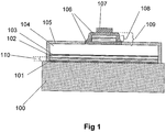
- a novel low loss bottom conductive multilayer reflector (CMR) stack, 110 is employed between the metal bottom contact, 101, and the p-GaN flip chip layer, 102.
- the layer 101 may also comprise a multilayer of electrical and thermal conducting metals optimised for maximal adhesion and highest optical reflectivity.
- the layer 101 resides on top of a conductive substrate 100, which also acts as the bottom p-contact.
- the CMR comprises at least 3 material layers, but may comprise 4 layers, 5 layers or more.
- the bottom CMR stack comprises transparent conductive materials. The materials of the layers in the CMR stack are selected and stacked to maximise the dielectric contrast between neighbouring layers. Hence, materials with alternating low and high refractive indexes are employed in the same stack.
- the reflectivity characteristics of the stack can be analysed by using the transfer matrix method (TMM) or other similar modelling technique.
- TMM transfer matrix method
- the CMR can comprise of any combination of multilayer stack design. It is an object of the invention to implement a high reflectivity multilayer stack that can reflect the largest percentage of trapped modes without introducing optical loss.
- Some examples of possible multilayer stack configurations are Omni-directional reflectors (ODR), periodic, aperiodic, binary, or quasiperiodic.
- the angle ⁇ i defines the propagation angle of the wavevector in the i -th layer.
- the transparent conductive materials in the bottom CMR stack can comprise multilayers of optically transparent metal oxides or nitrides such as, but not limited to, ZnO, Indium Tin Oxide (ITO), Titanium oxide, GaN or Carbon Nanotubes (CNT) or transparent conductive metal oxides with a spinel crystal structure.
- Such materials typically possess high refractive indexes of approximately between 1.8 and 2.45. These materials provide suitable candidates for the high refractive index layers in the CMR stack.
- the index value of the high refractive index material can also exceed that of the light emitting region, for example up to 2.6, or up to 2.8.
- metal oxides or nitrides or oxyntrides with higher porosity such as ITO nanorods, GaN nanocolumns, AIN nanocolumns, ZnO doped with Silicon or MgF can be deposited, providing a low refractive index of around 1.3.
- Transparent conductive polymer materials can also be used. Examples of these include poly(ethylenedioxythiophene):poly(styrenesulfonate) (PEDOT:PSS) or polyaniline:poly(styrenesulfonate) (PANI:PSS), having refractive indexes of about 1.5.
- the refractive index of the low refractive index material can reside between 1.0 and that of the index of the light emitting material, which in the case of GaN is 2.45.
- the vertical type light emitting device structure of the present invention further comprises an n-type GaN layer, 104, as well as the light emitting Multiple Quantum Well region, 103, sandwiched between layer 102 and 104.
- the top multilayer metal n-contact region, 107 is deposited on top of another CMR stack region, 109.
- the multilayer of metal can comprise a thin adhesion layer to reduce contact resistance followed by a reflective metallic layer followed by a metallic electrode.
- the top CMR stack is incorporated to reduce the photon absorption and total light output attenuation from the light emitted under the top contact region.
- the top electrode layer extends across a proportion of the area of the light extracting surface of the second semiconductor layer that is more than 1%, preferably more than 3%, more preferably more than 5%, even more preferably more than 10%, still more preferably more than 25%, and most preferably more than 50%. Hence, if the light emerging from under these regions can be allowed to escape with minimum loss, then an increase in the total luminous output of the LED can be achieved.
- the top CMR stack, 109 can comprise of similar transparent conductive materials used in the bottom CMR stack 110.
- another object of the present invention is to provide a CMR stack of mainly dielectric materials, 108, surrounded by a transparent conductive material, 106.
- the layer 108 comprises of at least 3 material layers, but may comprise of 4 layers, 5 layers or more.
- the multilayer 108 is optimised for maximum omnidirectional reflectivity, while the layer 106 is selected for optical transparency and maximal electrical conductivity.
- Layer 106 can comprise of similar materials selected for use in CMR 110, while for layer 108 a much wider selection of optically transparent dielectrics commonly employed for optical coatings can be selected.
- the conductive layer 106 resides on top of the n-GaN surface to provide a good electrical contact, as well as overcoating the multilayer 106 to provide a path for electrical current to propagate from contact 107 to the n-GaN material 104.
- the final light emitting device is surrounded by a passivation layer, 105, to protect the GaN material from the environment and from oxidation.
- the passivation material may comprise Silicon Dioxide, Silicon Nitride or a polymer layer, although other materials are possible.
- the top CMR stack, 206 can comprise of transparent conductive materials similar to those in bottom stack 110.
- the CMR stack 206 is designed, and constituent materials are selected in a similar way, to the bottom CMR stack 110.
- a 3-layer multilayer stack is implemented.
- the first layer 200 can comprise, for example, of a low refractive index material such as doped ZnO, followed by a layer 201 of higher refractive index ITO, followed by a layer 202 of a lower refractive index material, e.g. doped ZnO.
- the thickness of each layer is optimised to provide maximal reflection of incident photons back into the GaN material.
- the transparent conductive surrounding overcoat is not required, since in this example the top n-type contact 204 may be deposited on top of a thin metal layer 203, which will perform similar functions to layer 101 in terms of improved adhesion and electrical conductivity.
- the top electrode density is increased to 5%, preferably 10%, more preferably 15%, and even more preferably 20% of the total top active surface of the LED device.
- the increased density allows improved current spreading along the n-GaN layer maintaining high injection efficiency even at high drive current of, for example, 1A, 1.5A, 2A, 2.5A, or 3A. Due to the novel low loss top electrodes the increased coverage will not to detrimental to the light extraction efficiency of the LED.
- An example plan view of the top electrode is sketched in the insert in Figure 2 . Two square pads at the bottom edge of the LED device exist for wire bonding. Cross connected electrodes across the top surface allows for improved even current spreading across the surface of the n-doped material 104. The spacing as well as width of electrodes directly relates to the efficiency of injecting the carriers at high current into the LED device.
- the top n-doped GaN material 104 is roughened to allow for increased probability of light escaping out of the top surface of the LED.
- Figure 3a shows an example of such roughening, using the device shown in Figure 1 , whereby the upper surface 300 of layer 104 is roughened.
- the roughening process introduces many scattering centres at the surface of the LED to allow light an increased chance of escape out of the top surface.
- the scattering centres increase the probability of photons incident on the roughened surface 300 lying inside the GaN-air escape cone angle.
- the roughening can take many different forms, including wet-etched pyramidal or inverted pyramidal structures on the surface of the GaN material, as-deposited clusters of high refractive index optically transparent dielectrics, or additionally as perturbed re-growth of a high refractive index materials. If small scale roughness, of the order of the emitted wavelength ( ⁇ / n GaN ) is introduced, trapped modes incident on the surface experience diffuse reflectivity as opposed to specular reflectivity, thereby increasing their chance of residing within the escape cone at the next multiple internal reflection.
- the top emission surface is randomly arranged with protruding pyramids ranging in size between approximately 0.5 ⁇ m and 2.5 ⁇ m, thereby providing high extraction efficiency for trapped waveguide modes.
- Top surface extraction enhancement factors of up to 2.5, 3.0, 3.5, 4.0, 5.0, or 6.0 may be realised, as compared to a bare, unroughened, unencapsulated LED with approximately 4.35% of the light emitted from the top surface.
- FIG. 3b another embodiment of a roughened top n-doped GaN surface is demonstrated.
- the n-GaN top surface region 301 under the top CMR contact is also roughened. This allows light that was specularly reflected by the top contact region to diffusely reflect back down, thereby increasing the probability of the light residing in the escape cone at the next incidence on the top roughened surface.
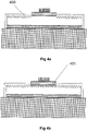
- Figures 4a and 4b show other exemplary illustrations of surface roughening employed in the embodiment of the present invention shown in Figure 1 .
- surface roughness 400 is applied to a LED with a top and bottom transparent CMR stack.
- the surface roughness is also applied to the top surface of the n-GaN region under the top CMR stack, as indicated by 401.
- FIGs 5a and 5b the benefits of the present invention are compared with prior art designs for top metal contacts.
- FIG 5a a prior art device with a top metal contact is illustrated.
- the metal contact, 502 adheres to the top of the n-GaN material of the LED structure, 500, by use of an adhesion layer 501.
- Electrical injection, 503, and carrier diffusion into the n-type material is achieved by the direct metal contact.
- trapped photons 504 incident on the metal contact 502 experience a large amount of optical loss, 507, and specular reflection 505 is greatly attenuated.
- Figure 5b an example of the operation of the present invention is demonstrated.
- the top transparent CMR stack 514 resides between the metal contact 512 and the LED n-type GaN material 500.
- a metal adhesion layer 511 between the 514 and 512 allows for improved adhesion between the metal contact and the 514 CMR stack.
- trapped photons 515 incident on the transparent CMR stack reside in the electromagnetic bandgap of the reflector and are forbidden to propagate through the stack 517 and onto the metal contact 512.
- the evanescent field set up inside the CMR stack, 514, due to the optically transparent reflector, allows a very low loss optical reflection 516 back into the GaN material.
- the transfer matrix method is used to determine the normal incidence reflectance of photons in the blue wavelength range.
- the typical examples illustrated in Figure 5a and Figure 5b are considered in particular.
- the reflectivity of different metal electrodes is compared in Table 2 in terms of the power reflectance in the blue wavelength range. From the selection of metals shown, the highest reflecting metals are Ag and Al, whereby approximately 11.3% and 16.7% respectively of loss is introduced at every reflectance, as indicated by 505 in Figure 5a . It is typical for light to undergo several reflections in the LED device prior to extraction and hence the overall loss experienced by the photons is typically many orders larger than the base figure quoted.
- the composition of the multilayer stack is highlighted in Table 3, including material, refractive index and thickness. The layers are listed in order of proximity to the underlying semiconductor layer 500. Layer numbers 1 to 4 listed in Table 3 lie in the CMR stack 514, while layer number 5 is the metal electrode layer 512 shown in Figure 5b . The total CMR thickness amounts to approximately 270nm with a reflectance of 98.5%. Table 3 Layer number Material Refractive index Thickness (nm) 1 Doped ZnO 1.3 85 2 ITO 2.1 55 3 Doped ZnO 1.3 85 4 ITO 2.1 85 5 electrode - Ag 0.15+ j 2.5 >50nm
- a light emitting module is formed by embedding a phosphor, 606, in an encapsulating material residing on top of a light emitting device of the present invention.
- the encapsulation comprises two layers of optically-transparent and environmentally-resistant material.
- the first encapsulation material, 605, that is disposed proximal to the light emitting device, is formed of a high refractive index material.
- the material is preferably textured or shaped to extract the maximum number of photons, but need not be.
- the encapsulant 605 can comprise a silicone material having a refractive index of approximately 2.1, 2.0, 1.8, or 1.6, but may have other refractive index or comprise other material.
- a high refractive index encapsulant allows a larger amount of light to escape from the roughened surface of the LED due to the larger escape cone angle.
- Texturing of the encapsulant can also be used to alter the far-field radiation profile of the LED. This may be in the form of a Fresnel lens or microlens texturing.
- the phosphor is subsequently disposed on the high refractive index encapsulant 605, while another encapsulation material 607, distal to the light emitting device, is disposed on the top of the phosphor.
- the phosphor 606 is located proximal, but not in contact with, the top n-GaN 604 LED material to avoid thermal heating of the phosphor and improve its lifetime.
- the phosphors may comprise of, but are not limited to, YAG:Ce, phosphors based on II-VI materials such as selenides, tellurides and sulphides and ZnS and InP, and also Europium doped Silicate phosphors, and Cerium and Terbium doped oxides and nitrides. In these examples, the combined emission from the phosphor and the LED are designed to emit the desired colour.
- the distal encapsulant 607 can also be shaped to provide the desired far field emission from the light emitting module.
- the shaping can vary from horizontally flat to hemispherical, for Lambertian emission, to parabolic for directional emission, and to other more complex shapes for many different desired far-field emission profiles.
- the encapsulant 607 also acts as a passivation layer to protect and seal the LED from environmental factors. Additionally, the encapsulant 605 and 607 may comprise the same material. Another passivation layer may also reside between the first encapsulation layer 605 and the LED device, as described in the method of manufacture below.
- the encapsulants can comprise, but are not limited to, silicone gels and resins and elastomers, ABS resins, epoxy, acrylates, spin on glass, PMMA, and thermoplastics and thermosetting resins.
- An adhesion layer and reflector layer, 608, such as Ni/Au, or Ag is deposited on top of layer 609.
- a metal contact, 610 is placed subsequently on layer 608. This acts as an electrode to spread current across the surface on the LED, as well as a region with an adhesion surface for wire bonding. Electrical contact is made by wire 611 contacting the top electrode, while the circuit is closed by making another contact with the conductive carrier 600.
- the light emitting module may be used for applications where white illumination is required, such as in solid state lighting. Other uses include architectural, medical or signage applications.
- the bottom and top CMR stack layers allows the light emitting device to be thinned down to a total thickness of less than 5 ⁇ m, preferably less than 3.5 ⁇ m, more preferably less than 3.0 ⁇ m, still more preferably less than 2.5 ⁇ m, even more preferably less than 2.0 ⁇ m, and most preferably less than 1.0 ⁇ m.
- This allows the LED to achieve high extraction efficiency while still maintaining high current injection.
- layers 104, 103 and 102 of the LED waveguide structure are reduced in thickness, thereby allowing fewer confined modes to reside in the waveguide and hence more efficient light extraction.
- a 3 micron structure will possess approximately 44 trapped modes while a thinner 1 micron LED structure can sustain approximately 15 trapped modes. Fewer modes allow surface extraction techniques such as roughening to perturb a large percentage of the trapped mode residing in the waveguide and hence will enable efficient coupling of the trapped mode into leaky modes and subsequent extraction over a short propagation distance.
- One drawback of reducing the thickness of the LED device is the reduction in the ability for the n-doped material 104, such as n-GaN, to spread carriers horizontally, which ultimately causes current crowding in the layer 104 and thus affects the injection efficiency of the LED. It is an object of the present invention that, by using the low loss conductive CMR stacks, an increased percentage coverage of the top electrodes is introduced to minimise current crowding and allow improved current injection and high drive current in thin LED devices. Top electrodes can be introduced at intervals of a minimum of 100 ⁇ m, 80 ⁇ m, 60 ⁇ m, 40 ⁇ m, or 20 ⁇ m.
- a method of manufacture of a vertical LED structure with a metallic substrate and reduced loss metal contact regions is proposed.
- the metal substrate provides both good thermal and electrical conduction during LED operation.
- Other benefits of vertical LED structures arise from the existence of one top metal contact rather than two, which effectively increases the active top emission area.
- the large area bottom metal contact also improves the electro-static discharge capabilities of the device.
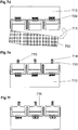
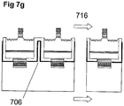
- An example of the complete process is shown in Figures 7a to 7g .
- Figure 7a shows an example of a GaN based LED epitaxially grown on a suitable growth wafer 700.
- the growth wafer can comprise, but is not limited to, Sapphire, Silicon Carbide, free-standing GaN or any other lattice matched material.
- the growth wafer can also comprise Si, as this is particularly beneficial when moving to larger six inch (152.4mm) wafer diameters.
- the LED device comprises at least n-type semiconductor layer 701, followed by an active light emitting region 702, subsequently followed by a top p-doped semiconductor material 703.
- the active region 702 can comprise a single quantum well (QW) region or multiple quantum wells (MQW). These layers are grown by conventional semiconductor growth techniques, such as metal organic vapour phase epitaxy (MOCVD), molecular beam epitaxy (MBE), or alternatively atomic layer deposition (ALD).
- MOCVD metal organic vapour phase epitaxy
- MBE molecular beam epitaxy
- ALD alternatively atomic layer deposition
- the layer can have a thickness of about 0.5 ⁇ m, about 1.5 ⁇ m, about 2.0 ⁇ m, about 2.5 ⁇ m, about 3 ⁇ m or about 4 ⁇ m.
- the MQW region 702 may comprise InGaN/GaN or AlGaN/GaN multilayer stacks. When these layers are forward biased they can emit light in the wavelength range between 240nm and 680nm.
- the thickness can vary between 5nm and 400nm, for example about 50nm, about 100nm, about 150nm, or about 180nm. It is important to note that the structure will be inverted and hence the current top surface will reside at the bottom of the device once the processing steps are complete.
- the bottom transparent CMR stack is then deposited.
- This can be carried out by any conventional deposition technique such as, but not limited to, any chemical vapour deposition technique (CVD), including low-pressure chemical vapour deposition (LPCVD), plasma-enhanced chemical vapour deposition (PECVD), atomic layer deposition (ALD), or other techniques such as sputtering or evaporation.
- CVD chemical vapour deposition technique
- LPCVD low-pressure chemical vapour deposition
- PECVD plasma-enhanced chemical vapour deposition
- ALD atomic layer deposition
- a first metallic low resistivity contact layer 705 is subsequently deposited on the structure. This layer also acts as a good adhesion layer between the metal permanent substrate and the underlying p-doped GaN or semiconductor region.
- This contact region preferably comprises one or more of Ni/Au, Ti/Au, Cr/Au, Au, Pd, Pt, Ru, Ni, Cr, ZnO, CNT, Ag, ITO, Al, and W, although other suitable materials may be used.
- a larger selection of conductive adhesion metal layers can be employed, since the reflector 704 resides between layer 705 and the p-GaN region 703 and therefore optically lossy metallic layers can also be utilised.
- the bottom contact region is defined lithographically and transferred into the transparent CMR stack and the metal layer as shown by 704 and 705 in figure 7b .
- the bottom contact region pattern may be etched by any etching technique suitable for materials residing in the transparent CMR stack and the metal 705, including wet etching or plasma etching, reactive ion etching (RIE) and inductively coupled plasma (ICP).
- the LED die regions are defined lithographically and etched to form trenches, 706, isolating the individual LED die, as shown in Figure 7b .
- the formation of the individual LED die prior to flip chip and growth wafer removal allows improved stress relief.
- a passivation layer 708 is then allowed to fill and overcoat the trenches 706.
- the passivation layer can comprise, but is not limited to, SiO 2 , Si 3 N 4 , polymer or spin-on-glass.
- a metal seed layer 707 is grown on top of the adhesion layer 705.
- the passivation layer acts to protect the GaN from environmental factors, as well as avoid the conductive seed layer shorting the LED structure.
- Layer 707 provides the seeding for any subsequent chemical plating process.
- This layer can comprise metals such as Cr, Cu, Pt, Au, Ag, Ti, Ni, and Pd.
- an additional metal adhesion layer 709 may optionally be deposited on the top surface of the passivation layer 708.
- the material can be selected from the same metals as for layer 705.
- the carrier metal substrate layer 710 is overgrown.
- This layer may comprise, but is not limited to, one of or a mixture of Au, Cu, Ni, Cr, Pt, Pd, In, and Al.
- the metal is grown by evaporation, sputtering, electroplating or electro-less plating.
- a thick layer of metal is formed with a thickness of approximately 20 ⁇ m, approximately 50 ⁇ m, approximately 100 ⁇ m, or approximately 150 ⁇ m.
- This thick layer 710 provides a rigid support to hold the underlying LED die during removal of the growth substrate 700.
- the removal process can be achieved by a selective etching process, a lift-off process such as laser lift-off, or a polishing method. A combination of such devices can also be implemented.
- the LED dies are flipped, as shown in Figure 7e .
- the new permanent carrier is now the thick metal layer 710 and the n-doped GaN or semiconductor material is the top exposed surface.
- the top conductive CMR stack is then deposited.
- the different layers in the multilayer stack are successively deposited using processes similar to those utilised for the bottom transparent CMR reflector.
- an adhesion layer is also deposited to assist with the bonding of the final top metal contact.
- An additional lithography and etch step is required at this stage to define the shape of the top transparent CMT stack. This will comprise similar processing steps to those used for CMR stack 704.
- an overcoating, conductive, optically-transparent layer is deposited to allow electrical conduction between the top metal contact 714 and the N-doped GaN layer 701, as shown in Figure 1 .
- the selection criteria for suitable materials and deposition techniques for the overcoating layer are identical to those of the top and bottom CMR layers.
- another lithography mask pattern transfer and an etch step is included to redefine the location of the overcoated top contact region and to remove any conductive layer that extends further than one of 1 ⁇ m, 2 ⁇ m, 3 ⁇ m, 5 ⁇ m, or 10 ⁇ m around the perimeter of the transparent CMR reflector 712.
- an n-type metal electrode contact pad 714 is patterned on top of the CMR stack 712 using a lift-off process.
- a lithography step and negative resist are employed to deposit the metal conformally on the top surface of the CMR stack.
- a wet or dry plasma etch are used to transfer the pattern into the resist.
- the n-GaN material is roughened. This can be accomplished by many techniques, such as wet anisotropic etching or photo-assisted wet etching.
- pyramids, inverted pyramids or whisker type roughness following the crystal plane of the GaN are formed by use of suitable chemicals, such as KOH.
- suitable chemicals such as KOH.
- the concentration, temperature, UV irradiation and biasing of the samples can all be controlled to assist in roughening the surface.
- the pyramid diameter is preferably between 0.5 ⁇ m and 2.5 ⁇ m.
- Nanoclusters of materials such as Si 3 N 4 or GaN crystals can be deposited on the surface of the n-GaN to improve light extraction.
- the individual LED die are separated along the trenches 706.
- the devices can subsequently be packaged with encapsulant and phosphors to produce complete solid state lighting modules, of the type shown in Figure 6 .
Landscapes
- Led Devices (AREA)
Claims (12)
- Dispositif électroluminescent comprenant :une première couche semi-conductrice (102) ayant un dopage d'un premier type ;une seconde couche semi-conductrice (104) ayant un dopage d'un second type ;une région électroluminescente (103) intercalée entre les première et seconde couches semi-conductrices (102, 104) ;une première couche d'électrode (101) disposée de manière proximale par rapport à la première couche semi-conductrice (102) et distale par rapport à la seconde couche semi-conductrice (104) ;une seconde couche d'électrode (107) disposée de manière proximale par rapport à la seconde couche semi-conductrice (104) et distale par rapport à la première couche semi-conductrice (102) ;une première pile formant réflecteur multicouche (110) intercalée entre la première couche d'électrode (101) et la première couche semi-conductrice (102), la première pile formant réflecteur multicouche (110) s'étendant au moins partiellement à travers une surface de la première couche semi-conductrice (102) et comprenant au moins une première couche disposée de manière proximale par rapport à la première couche d'électrode (102) et une dernière couche disposée de manière distale par rapport à la première couche d'électrode (102) ; etune seconde pile formant réflecteur multicouche (109) intercalée entre la seconde couche d'électrode (107) et la seconde couche semi-conductrice (104), la seconde pile formant réflecteur multicouche (109) s'étendant uniquement partiellement à travers une surface de la seconde couche semi-conductrice (104) et comprenant au moins une première couche disposée de manière distale par rapport à la seconde couche d'électrode (107) et une dernière couche disposée de manière proximale par rapport à la seconde couche d'électrode (107),dans lequel :au moins la première et la dernière couche de la première pile formant réflecteur multicouche (110) sont électroconductrices et optiquement transparentes et au moins la première couche et la dernière couche de la seconde pile formant réflecteur multicouche (109) sont électroconductrices et optiquement transparentes ;la seconde pile formant réflecteur multicouche (109, 206) s'étend à travers au moins la même partie de la surface de la seconde couche semi-conductrice (104) à travers laquelle s'étend également la seconde couche d'électrode (107) ; etl'étendue transversale de la seconde pile formant réflecteur multicouche (109) est inférieure à celle de la première pile formant réflecteur multicouche (110), et la lumière générée dans la région électroluminescente (103) est extraite du dispositif à travers ces parties de la surface de la seconde couche semi-conductrice (104) opposée à la première pile formant réflecteur multicouche (110) mais à travers laquelle ne s'étend pas la seconde pile formant réflecteur multicouche (109),caractérisé en ce que :au moins 60 % de la lumière incidente sur la première pile formant réflecteur multicouche (110) qui est générée dans la région électroluminescente (103) est réfléchie par la première pile (110) et au moins 60 % de la lumière incidente sur la seconde pile formant réflecteur multicouche (109) qui est générée dans la région électroluminescente (103) est réfléchie par la seconde pile (109) ;la seconde pile formant réflecteur multicouche (109) comprend une pile multicouche (108) d'au moins trois couches et qui est optimisée pour une réflectivité omnidirectionnelle maximale ; etla seconde pile formant réflecteur multicouche (109) comprend en outre une couche (106) de matériau optiquement transparent et électroconducteur qui entoure la pile multicouche (108).
- Dispositif électroluminescent selon la revendication 1, dans lequel :la première et/ou la seconde pile formant réflecteur multicouche (110, 109) comprend au moins 3 couches, de préférence, au moins 4 couches, et de manière préférée entre toutes, au moins 5 couches ; etla première et/ou la seconde pile formant réflecteur multicouche (110, 109) comprend au moins deux indices de réfraction optiques différents.
- Dispositif électroluminescent selon l'une quelconque des revendications précédentes, dans lequel au moins la première couche et la dernière couche et la première et/ou la seconde pile formant réflecteur multicouche (110, 109) sont en contact électrique afin d'obtenir une conduction électrique entre la première et la dernière couche de la pile respective.
- Dispositif électroluminescent selon l'une quelconque des revendications précédentes, dans lequel la seconde couche d'électrode (107) s'étend à travers une proportion de la zone de la surface d'extraction de lumière de la seconde couche semi-conductrice (104) qui est supérieure à 1 %, de préférence, supérieure à 3 %, de préférence encore, supérieure à 5 %, encore plus préférablement, supérieure à 10 %, de manière encore davantage préférée, supérieure à 25 %, et de manière préférée entre toutes, supérieure à 50 %.
- Dispositif électroluminescent selon l'une quelconque des revendications précédentes, dans lequel la première et/ou la seconde pile formant réflecteur multicouche (110, 109) comprend un matériau diélectrique choisi dans un groupe qui inclut le fluorure de magnésium, le nitrure de silicium, le dioxyde de silicium et les oxydes, nitrures et/ou oxynitrures métalliques dérivés d'un groupe de métaux constitué de l'aluminium, du hafnium, du tantale, du titane, du chrome et du zirconium.
- Dispositif électroluminescent selon l'une quelconque des revendications précédentes, dans lequel les couches électroconductrices et optiquement transparentes dans la première et/ou la seconde pile formant réflecteur multicouche (110, 109) comprennent un matériau choisi dans le groupe constitué de ZnO, oxyde étain-indium (ITO), GaN, nanotubes de carbone (CNT), oxyde de métal conducteur transparent, nitrure conducteur transparent, oxyde conducteur transparent avec structure de cristaux de spinelle, nanotiges d'ITO, nanocolonnes de GaN, nanocolonnes d'AIN, ZnO dopé avec du silicium, polymère conducteur transparent, poly(éthylènedioxythiophène) : poly(styrènesulfonate) (PEDOT:PSS), et polyaniline : poly(styrènesulfonate) (PANI:PSS).
- Dispositif électroluminescent selon l'une quelconque des revendications précédentes, dans lequel la surface (300, 400) de la seconde couche semi-conductrice (104) à travers laquelle est extraite la lumière est au moins partiellement rugosifiée (301, 401) pour augmenter l'extraction de lumière.
- Dispositif électroluminescent selon l'une quelconque des revendications précédentes, dans lequel l'épaisseur combinée totale de la première couche semi-conductrice (102), de la seconde couche semi-conductrice (104) et de la région électroluminescente (103) est inférieure à 3,5 micron, de préférence, inférieure à 3,0 micron, plus préférablement, inférieure à 2,5 micron, encore plus préférablement, inférieure à 2,0 micron, et de manière préférée entre toutes, inférieure à 1,5 micron.
- Dispositif électroluminescent selon l'une quelconque des revendications précédentes, dans lequel les surfaces exposées de la première couche semi-conductrice (102), de la seconde couche semi-conductrice (104) et de la région électroluminescente (103) sont au moins partiellement recouvertes d'une couche de passivation (105) pour protéger le dispositif électroluminescent.
- Module électroluminescent pour applications d'éclairage à semi-conducteurs, ledit module comprenant :un dispositif électroluminescent selon l'une quelconque des revendications précédentes;un premier matériau d'encapsulation (605) couvrant au moins la surface d'extraction de lumière de la seconde couche semi-conductrice (604) ;un second matériau d'encapsulation (607) recouvrant au moins le premier matériau d'encapsulation (605) ; etun matériau de phosphore (606) intercalé entre les premier et second matériaux d'encapsulation (605, 607).
- Module électroluminescent selon la revendication 10, dans lequel au moins une partie de surface du premier matériau d'encapsulation (605) distale par rapport à la surface d'extraction de lumière de la seconde couche semi-conductrice (604) est texturée pour une extraction de lumière maximale.
- Procédé de fabrication d'un dispositif électroluminescent selon l'une quelconque des revendications 1 à 9, ou d'un module électroluminescent selon la revendication 10 ou la revendication 11, le procédé comprenant les étapes suivantes :la croissance de chacun d'un second matériau semi-conducteur (703), de la région électroluminescente (702) et d'un premier matériau semi-conducteur (701) ;le dépôt d'une première pile formant réflecteur multicouche (704) ;la formation de tranchées d'isolation mésa (706) dans le dispositif électroluminescent ;le dépôt d'une couche de passivation (708) ;le dépôt d'une première électrode (705) ;la fixation d'une embase conductrice (710) ;le retrait du substrat de croissance (700) ;le dépôt d'une seconde pile formant réflecteur multicouche (712) ;le dépôt d'une couche de matériau optiquement transparent et électroconducteur pour recouvrir la seconde pile multicouche ;le dépôt d'une seconde électrode (714) ;la rugosification d'une surface supérieure de la seconde couche semi-conductrice (715) ;
etla séparation d'une puce électroluminescente isolée (716).
Applications Claiming Priority (2)
| Application Number | Priority Date | Filing Date | Title |
|---|---|---|---|
| GB0704120A GB2447091B8 (en) | 2007-03-02 | 2007-03-02 | Vertical light emitting diodes |
| PCT/GB2008/000710 WO2008107654A1 (fr) | 2007-03-02 | 2008-03-03 | Diodes électroluminescentes verticales |
Publications (2)
| Publication Number | Publication Date |
|---|---|
| EP2135304A1 EP2135304A1 (fr) | 2009-12-23 |
| EP2135304B1 true EP2135304B1 (fr) | 2018-02-28 |
Family
ID=37965849
Family Applications (1)
| Application Number | Title | Priority Date | Filing Date |
|---|---|---|---|
| EP08718588.0A Active EP2135304B1 (fr) | 2007-03-02 | 2008-03-03 | Diodes électroluminescentes verticales |
Country Status (5)
| Country | Link |
|---|---|
| US (2) | US8592842B2 (fr) |
| EP (1) | EP2135304B1 (fr) |
| CN (1) | CN101636852B (fr) |
| GB (1) | GB2447091B8 (fr) |
| WO (1) | WO2008107654A1 (fr) |
Cited By (1)
| Publication number | Priority date | Publication date | Assignee | Title |
|---|---|---|---|---|
| WO2023072408A1 (fr) * | 2021-10-29 | 2023-05-04 | Ams-Osram International Gmbh | Dispositif optoélectronique et son procédé de traitement |
Families Citing this family (48)
| Publication number | Priority date | Publication date | Assignee | Title |
|---|---|---|---|---|
| GB2447091B8 (en) * | 2007-03-02 | 2010-01-13 | Photonstar Led Ltd | Vertical light emitting diodes |
| US7915629B2 (en) * | 2008-12-08 | 2011-03-29 | Cree, Inc. | Composite high reflectivity layer |
| US9461201B2 (en) | 2007-11-14 | 2016-10-04 | Cree, Inc. | Light emitting diode dielectric mirror |
| KR101449030B1 (ko) * | 2008-04-05 | 2014-10-08 | 엘지이노텍 주식회사 | 그룹 3족 질화물계 반도체 발광다이오드 소자 및 이의 제조방법 |
| DE102008051048A1 (de) * | 2008-10-09 | 2010-04-15 | Osram Opto Semiconductors Gmbh | Optoelektronischer Halbleiterkörper |
| US7868347B2 (en) * | 2009-03-15 | 2011-01-11 | Sky Advanced LED Technologies Inc | Metal core multi-LED SMD package and method of producing the same |
| FI122622B (fi) * | 2009-06-05 | 2012-04-30 | Optogan Oy | Valoa emittoiva puolijohdelaite ja valmistusmenetelmä |
| US9362459B2 (en) | 2009-09-02 | 2016-06-07 | United States Department Of Energy | High reflectivity mirrors and method for making same |
| KR100986407B1 (ko) * | 2009-10-22 | 2010-10-08 | 엘지이노텍 주식회사 | 발광소자 및 그 제조방법 |
| US9435493B2 (en) | 2009-10-27 | 2016-09-06 | Cree, Inc. | Hybrid reflector system for lighting device |
| DE102009058796A1 (de) | 2009-12-18 | 2011-06-22 | OSRAM Opto Semiconductors GmbH, 93055 | Optoelektronisches Bauelement und Verfahren zur Herstellung eines optoelektronischen Bauelements |
| KR101047721B1 (ko) | 2010-03-09 | 2011-07-08 | 엘지이노텍 주식회사 | 발광 소자, 발광 소자 제조방법 및 발광 소자 패키지 |
| US9012938B2 (en) | 2010-04-09 | 2015-04-21 | Cree, Inc. | High reflective substrate of light emitting devices with improved light output |
| US9105824B2 (en) | 2010-04-09 | 2015-08-11 | Cree, Inc. | High reflective board or substrate for LEDs |
| IT1399507B1 (it) | 2010-04-21 | 2013-04-19 | Getters Spa | Lampada a scarica migliorata |
| KR101039939B1 (ko) * | 2010-04-28 | 2011-06-09 | 엘지이노텍 주식회사 | 발광소자, 발광소자의 제조방법, 발광소자 패키지 및 이를 포함하는 조명시스템 |
| US8598614B2 (en) * | 2010-08-30 | 2013-12-03 | Epistar Corporation | Light-emitting devices |
| EP2668034A4 (fr) * | 2011-01-27 | 2016-07-06 | Vitriflex Inc | Empilement multicouche inorganique, procédés et compositions associés |
| US8536594B2 (en) | 2011-01-28 | 2013-09-17 | Micron Technology, Inc. | Solid state lighting devices with reduced dimensions and methods of manufacturing |
| DE102011013821B4 (de) * | 2011-03-14 | 2024-05-23 | OSRAM Opto Semiconductors Gesellschaft mit beschränkter Haftung | Verfahren zur Herstellung zumindest eines optoelektronischen Halbleiterchips |
| JPWO2012123997A1 (ja) * | 2011-03-17 | 2014-07-17 | パナソニック株式会社 | 半導体発光素子及びそれを用いた発光装置 |
| DE102011016302B4 (de) | 2011-04-07 | 2026-01-15 | OSRAM Opto Semiconductors Gesellschaft mit beschränkter Haftung | Optoelektronischer Halbleiterchip |
| US9728676B2 (en) | 2011-06-24 | 2017-08-08 | Cree, Inc. | High voltage monolithic LED chip |
| US10243121B2 (en) | 2011-06-24 | 2019-03-26 | Cree, Inc. | High voltage monolithic LED chip with improved reliability |
| US9178114B2 (en) | 2011-09-29 | 2015-11-03 | Manutius Ip, Inc. | P-type doping layers for use with light emitting devices |
| US8698163B2 (en) | 2011-09-29 | 2014-04-15 | Toshiba Techno Center Inc. | P-type doping layers for use with light emitting devices |
| US20130082274A1 (en) | 2011-09-29 | 2013-04-04 | Bridgelux, Inc. | Light emitting devices having dislocation density maintaining buffer layers |
| US8853668B2 (en) | 2011-09-29 | 2014-10-07 | Kabushiki Kaisha Toshiba | Light emitting regions for use with light emitting devices |
| US8664679B2 (en) | 2011-09-29 | 2014-03-04 | Toshiba Techno Center Inc. | Light emitting devices having light coupling layers with recessed electrodes |
| US9012921B2 (en) | 2011-09-29 | 2015-04-21 | Kabushiki Kaisha Toshiba | Light emitting devices having light coupling layers |
| JP2013125816A (ja) * | 2011-12-14 | 2013-06-24 | Toshiba Corp | 半導体発光素子 |
| WO2013112435A1 (fr) | 2012-01-24 | 2013-08-01 | Cooledge Lighting Inc. | Dispositifs électroluminescents présentant des puces distinctes à luminophore et procédés de fabrication associés |
| US8896010B2 (en) | 2012-01-24 | 2014-11-25 | Cooledge Lighting Inc. | Wafer-level flip chip device packages and related methods |
| US8907362B2 (en) | 2012-01-24 | 2014-12-09 | Cooledge Lighting Inc. | Light-emitting dies incorporating wavelength-conversion materials and related methods |
| KR101784849B1 (ko) * | 2013-01-04 | 2017-10-13 | 삼성전자주식회사 | 다층 투명 전극을 갖는 발광 소자 및 그 제조 방법 |
| US10666017B2 (en) * | 2013-02-20 | 2020-05-26 | Vertically Integrated (Vi) Systems Gmbh | Optoelectronic device based on a surface-trapped optical mode |
| CN104051664A (zh) * | 2013-03-12 | 2014-09-17 | 海洋王照明科技股份有限公司 | 一种有机电致发光器件及其制备方法 |
| WO2015119858A1 (fr) | 2014-02-05 | 2015-08-13 | Cooledge Lighting Inc. | Puces électroluminescentes contenant des matériaux de conversion de longueurs d'ondes et procédés y relatifs |
| US10658546B2 (en) | 2015-01-21 | 2020-05-19 | Cree, Inc. | High efficiency LEDs and methods of manufacturing |
| US10217914B2 (en) * | 2015-05-27 | 2019-02-26 | Samsung Electronics Co., Ltd. | Semiconductor light emitting device |
| CN108369977B (zh) * | 2015-10-01 | 2021-06-15 | 克利公司 | 低光学损失倒装芯片固态照明设备 |
| CN106252469A (zh) * | 2016-08-29 | 2016-12-21 | 广东德力光电有限公司 | 一种应用复合掩膜的led晶胞制造方法 |
| DE102017101729A1 (de) * | 2017-01-30 | 2018-08-02 | Osram Opto Semiconductors Gmbh | Strahlungsemittierende Vorrichtung |
| CN108735868B (zh) * | 2017-04-25 | 2019-10-25 | 山东浪潮华光光电子股份有限公司 | 一种GaN基LED包覆式电极结构的制作方法 |
| US11031527B2 (en) | 2018-01-29 | 2021-06-08 | Creeled, Inc. | Reflective layers for light-emitting diodes |
| GB2595684A (en) * | 2020-06-03 | 2021-12-08 | Plessey Semiconductors Ltd | Spacer LED architecture for high efficiency micro LED displays |
| US11569414B2 (en) | 2021-02-17 | 2023-01-31 | Meta Platforms Technologies, Llc | Self-aligned ITO DBR based p-contact for small pitch micro-LED |
| CN119230681B (zh) * | 2023-06-29 | 2025-11-28 | 厦门三安光电有限公司 | 发光二极管及发光装置 |
Citations (2)
| Publication number | Priority date | Publication date | Assignee | Title |
|---|---|---|---|---|
| US5414281A (en) * | 1992-08-25 | 1995-05-09 | Mitsubishi Cable Industries, Ltd. | Semiconductor light emitting element with reflecting layers |
| EP0951076A2 (fr) * | 1998-04-17 | 1999-10-20 | Hewlett-Packard Company | Réflecteurs enterrés dans un matériau épitaxial pour des dispositifs émetteurs de lumière et méthode de fabrication |
Family Cites Families (28)
| Publication number | Priority date | Publication date | Assignee | Title |
|---|---|---|---|---|
| US5568499A (en) * | 1995-04-07 | 1996-10-22 | Sandia Corporation | Optical device with low electrical and thermal resistance bragg reflectors |
| US5874747A (en) * | 1996-02-05 | 1999-02-23 | Advanced Technology Materials, Inc. | High brightness electroluminescent device emitting in the green to ultraviolet spectrum and method of making the same |
| US5779924A (en) * | 1996-03-22 | 1998-07-14 | Hewlett-Packard Company | Ordered interface texturing for a light emitting device |
| US6229160B1 (en) * | 1997-06-03 | 2001-05-08 | Lumileds Lighting, U.S., Llc | Light extraction from a semiconductor light-emitting device via chip shaping |
| US5962971A (en) * | 1997-08-29 | 1999-10-05 | Chen; Hsing | LED structure with ultraviolet-light emission chip and multilayered resins to generate various colored lights |
| US6015719A (en) * | 1997-10-24 | 2000-01-18 | Hewlett-Packard Company | Transparent substrate light emitting diodes with directed light output |
| US6992334B1 (en) | 1999-12-22 | 2006-01-31 | Lumileds Lighting U.S., Llc | Multi-layer highly reflective ohmic contacts for semiconductor devices |
| EP2270875B1 (fr) * | 2000-04-26 | 2018-01-10 | OSRAM Opto Semiconductors GmbH | Dispositf à semiconducteur émetteur de lumière et son procédé de fabrication |
| JP2002111054A (ja) * | 2000-09-29 | 2002-04-12 | Toshiba Corp | 垂直共振器型半導体発光素子及び垂直共振器型半導体発光装置 |
| US6998281B2 (en) * | 2000-10-12 | 2006-02-14 | General Electric Company | Solid state lighting device with reduced form factor including LED with directional emission and package with microoptics |
| US6784462B2 (en) * | 2001-12-13 | 2004-08-31 | Rensselaer Polytechnic Institute | Light-emitting diode with planar omni-directional reflector |
| US6455340B1 (en) * | 2001-12-21 | 2002-09-24 | Xerox Corporation | Method of fabricating GaN semiconductor structures using laser-assisted epitaxial liftoff |
| DE10208171A1 (de) * | 2002-02-26 | 2003-09-18 | Osram Opto Semiconductors Gmbh | Strahlungsemittierendes Halbleiterbauelement mit vertikaler Emissionsrichtung und Herstellungsverfahren dafür |
| TW569479B (en) * | 2002-12-20 | 2004-01-01 | Ind Tech Res Inst | White-light LED applying omnidirectional reflector |
| US6884646B1 (en) * | 2004-03-10 | 2005-04-26 | Uni Light Technology Inc. | Method for forming an LED device with a metallic substrate |
| US7432119B2 (en) * | 2005-01-11 | 2008-10-07 | Semileds Corporation | Light emitting diode with conducting metal substrate |
| US20070170596A1 (en) * | 2006-01-26 | 2007-07-26 | Way-Jze Wen | Flip-chip light emitting diode with high light-emitting efficiency |
| US7829905B2 (en) * | 2006-09-07 | 2010-11-09 | Hong Kong Applied Science And Technology Research Institute Co., Ltd. | Semiconductor light emitting device |
| GB2447091B8 (en) * | 2007-03-02 | 2010-01-13 | Photonstar Led Ltd | Vertical light emitting diodes |
| US20080217634A1 (en) * | 2007-03-06 | 2008-09-11 | Wen-Huang Liu | Vertical light-emitting diode structure with omni-directional reflector |
| GB0717802D0 (en) * | 2007-09-12 | 2007-10-24 | Photonstar Led Ltd | Electrically isolated vertical light emitting diode structure |
| GB2462411B (en) * | 2008-07-30 | 2013-05-22 | Photonstar Led Ltd | Tunable colour led module |
| US8143636B2 (en) * | 2008-11-18 | 2012-03-27 | Epistar Corporation | Light-emitting device |
| US8017963B2 (en) * | 2008-12-08 | 2011-09-13 | Cree, Inc. | Light emitting diode with a dielectric mirror having a lateral configuration |
| TW201041190A (en) * | 2009-05-01 | 2010-11-16 | Univ Nat Taiwan Science Tech | Polarized white light emitting diode (LED) |
| KR101028327B1 (ko) * | 2010-04-15 | 2011-04-12 | 엘지이노텍 주식회사 | 발광소자, 발광소자 제조방법 및 발광소자 패키지 |
| CN102386200B (zh) * | 2010-08-27 | 2014-12-31 | 财团法人工业技术研究院 | 发光单元阵列与投影系统 |
| US20150008465A1 (en) * | 2013-07-08 | 2015-01-08 | Invenlux Corporation | Reflective electrode structure, light emitting device and package |
-
2007
- 2007-03-02 GB GB0704120A patent/GB2447091B8/en active Active
-
2008
- 2008-03-03 US US12/529,098 patent/US8592842B2/en active Active
- 2008-03-03 WO PCT/GB2008/000710 patent/WO2008107654A1/fr not_active Ceased
- 2008-03-03 EP EP08718588.0A patent/EP2135304B1/fr active Active
- 2008-03-03 CN CN2008800069828A patent/CN101636852B/zh active Active
-
2013
- 2013-10-31 US US14/068,673 patent/US9178119B2/en active Active
Patent Citations (2)
| Publication number | Priority date | Publication date | Assignee | Title |
|---|---|---|---|---|
| US5414281A (en) * | 1992-08-25 | 1995-05-09 | Mitsubishi Cable Industries, Ltd. | Semiconductor light emitting element with reflecting layers |
| EP0951076A2 (fr) * | 1998-04-17 | 1999-10-20 | Hewlett-Packard Company | Réflecteurs enterrés dans un matériau épitaxial pour des dispositifs émetteurs de lumière et méthode de fabrication |
Non-Patent Citations (1)
| Title |
|---|
| C.H. LIN ET AL: "Enhancement of InGaN-GaN Indium-Tin-Oxide Flip-Chip Light-Emitting Diodes With TiO2-SiO2 Multilayer Stack Omnidirectional Reflector", IEEE PHOTONICS TECHNOLOGY LETTERS., vol. 18, no. 19, 1 October 2006 (2006-10-01), US, pages 2050 - 2052, XP055318572, ISSN: 1041-1135, DOI: 10.1109/LPT.2006.883330 * |
Cited By (1)
| Publication number | Priority date | Publication date | Assignee | Title |
|---|---|---|---|---|
| WO2023072408A1 (fr) * | 2021-10-29 | 2023-05-04 | Ams-Osram International Gmbh | Dispositif optoélectronique et son procédé de traitement |
Also Published As
| Publication number | Publication date |
|---|---|
| EP2135304A1 (fr) | 2009-12-23 |
| US20100038669A1 (en) | 2010-02-18 |
| WO2008107654A1 (fr) | 2008-09-12 |
| US9178119B2 (en) | 2015-11-03 |
| US8592842B2 (en) | 2013-11-26 |
| GB2447091B8 (en) | 2010-01-13 |
| GB2447091A (en) | 2008-09-03 |
| CN101636852A (zh) | 2010-01-27 |
| GB2447091B (en) | 2009-12-23 |
| GB0704120D0 (en) | 2007-04-11 |
| CN101636852B (zh) | 2012-06-20 |
| US20140054625A1 (en) | 2014-02-27 |
Similar Documents
| Publication | Publication Date | Title |
|---|---|---|
| US8592842B2 (en) | Vertical light emitting diodes | |
| EP2176891B1 (fr) | Del verticale à trous d'interconnexion conducteurs | |
| EP2220696B1 (fr) | Diode électroluminescente a extraction de lumière améliorée | |
| EP1526583B1 (fr) | Elément luminescent à crystal photonique | |
| US9263652B2 (en) | Semiconductor light-emitting device | |
| US20070018184A1 (en) | Light emitting diodes with high light extraction and high reflectivity | |
| TW437104B (en) | Semiconductor light-emitting device and method for manufacturing the same | |
| US20030222263A1 (en) | High-efficiency light-emitting diodes | |
| US20160336482A1 (en) | Light-emitting device | |
| WO2008021988A2 (fr) | DEL À BASE DE GAN AVEC UNE EFFICACITÉ D'EXTRACTION DE LUMIÈRE amÉliorÉe ET PROCÉDÉ PERMETTANT DE LE PRODUIRE | |
| TW202029529A (zh) | 發光元件及其製造方法 | |
| US12132152B2 (en) | Light-emitting diode | |
| US20150311400A1 (en) | Light-emitting device | |
| CN102082216B (zh) | 一种发光二极管芯片及其制造方法 | |
| CN216624313U (zh) | 一种具有波导应变的外延结构、led芯片 | |
| CN114078990A (zh) | 一种具有波导应变的外延结构、led芯片及制作方法 | |
| US20250386619A1 (en) | Light-directing structures in light-emitting diode devices and related methods | |
| US20230411562A1 (en) | Light extraction structures for light-emitting diode chips and related methods | |
| US20250133876A1 (en) | Light-emitting diode chips with light extraction films and related methods | |
| US20250031487A1 (en) | Light-emitting diode | |
| CN118943266B (zh) | 发光二极管及发光装置 | |
| JP2024544882A (ja) | オプトエレクトロニクス半導体部品 | |
| CN114220894A (zh) | 一种不可见光发光二极管及其制备方法 |
Legal Events
| Date | Code | Title | Description |
|---|---|---|---|
| PUAI | Public reference made under article 153(3) epc to a published international application that has entered the european phase |
Free format text: ORIGINAL CODE: 0009012 |
|
| 17P | Request for examination filed |
Effective date: 20091002 |
|
| AK | Designated contracting states |
Kind code of ref document: A1 Designated state(s): AT BE BG CH CY CZ DE DK EE ES FI FR GB GR HR HU IE IS IT LI LT LU LV MC MT NL NO PL PT RO SE SI SK TR |
|
| RAP1 | Party data changed (applicant data changed or rights of an application transferred) |
Owner name: PHOTONSTAR LED LIMITED |
|
| DAX | Request for extension of the european patent (deleted) | ||
| STAA | Information on the status of an ep patent application or granted ep patent |
Free format text: STATUS: EXAMINATION IS IN PROGRESS |
|
| 17Q | First examination report despatched |
Effective date: 20161118 |
|
| REG | Reference to a national code |
Ref country code: DE Ref legal event code: R079 Ref document number: 602008054200 Country of ref document: DE Free format text: PREVIOUS MAIN CLASS: H01L0033000000 Ipc: H01L0033100000 |
|
| RIC1 | Information provided on ipc code assigned before grant |
Ipc: H01L 33/38 20100101ALN20170731BHEP Ipc: H01L 33/44 20100101ALN20170731BHEP Ipc: H01L 33/46 20100101ALI20170731BHEP Ipc: H01L 33/22 20100101ALN20170731BHEP Ipc: H01L 33/10 20100101AFI20170731BHEP Ipc: H01L 33/50 20100101ALN20170731BHEP Ipc: H01L 33/00 20100101ALI20170731BHEP Ipc: H01L 33/42 20100101ALI20170731BHEP Ipc: H01L 33/40 20100101ALN20170731BHEP |
|
| GRAP | Despatch of communication of intention to grant a patent |
Free format text: ORIGINAL CODE: EPIDOSNIGR1 |
|
| STAA | Information on the status of an ep patent application or granted ep patent |
Free format text: STATUS: GRANT OF PATENT IS INTENDED |
|
| RAP1 | Party data changed (applicant data changed or rights of an application transferred) |
Owner name: LUMILEDS HOLDING B.V. |
|
| INTG | Intention to grant announced |
Effective date: 20171116 |
|
| GRAS | Grant fee paid |
Free format text: ORIGINAL CODE: EPIDOSNIGR3 |
|
| GRAA | (expected) grant |
Free format text: ORIGINAL CODE: 0009210 |
|
| STAA | Information on the status of an ep patent application or granted ep patent |
Free format text: STATUS: THE PATENT HAS BEEN GRANTED |
|
| AK | Designated contracting states |
Kind code of ref document: B1 Designated state(s): AT BE BG CH CY CZ DE DK EE ES FI FR GB GR HR HU IE IS IT LI LT LU LV MC MT NL NO PL PT RO SE SI SK TR |
|
| REG | Reference to a national code |
Ref country code: GB Ref legal event code: FG4D Ref country code: CH Ref legal event code: EP |
|
| REG | Reference to a national code |
Ref country code: AT Ref legal event code: REF Ref document number: 975039 Country of ref document: AT Kind code of ref document: T Effective date: 20180315 |
|
| REG | Reference to a national code |
Ref country code: IE Ref legal event code: FG4D |
|
| REG | Reference to a national code |
Ref country code: DE Ref legal event code: R096 Ref document number: 602008054200 Country of ref document: DE Ref country code: FR Ref legal event code: PLFP Year of fee payment: 11 |
|
| REG | Reference to a national code |
Ref country code: NL Ref legal event code: MP Effective date: 20180228 |
|
| REG | Reference to a national code |
Ref country code: LT Ref legal event code: MG4D |
|
| REG | Reference to a national code |
Ref country code: AT Ref legal event code: MK05 Ref document number: 975039 Country of ref document: AT Kind code of ref document: T Effective date: 20180228 |
|
| PG25 | Lapsed in a contracting state [announced via postgrant information from national office to epo] |
Ref country code: ES Free format text: LAPSE BECAUSE OF FAILURE TO SUBMIT A TRANSLATION OF THE DESCRIPTION OR TO PAY THE FEE WITHIN THE PRESCRIBED TIME-LIMIT Effective date: 20180228 Ref country code: NL Free format text: LAPSE BECAUSE OF FAILURE TO SUBMIT A TRANSLATION OF THE DESCRIPTION OR TO PAY THE FEE WITHIN THE PRESCRIBED TIME-LIMIT Effective date: 20180228 Ref country code: CY Free format text: LAPSE BECAUSE OF FAILURE TO SUBMIT A TRANSLATION OF THE DESCRIPTION OR TO PAY THE FEE WITHIN THE PRESCRIBED TIME-LIMIT Effective date: 20180228 Ref country code: NO Free format text: LAPSE BECAUSE OF FAILURE TO SUBMIT A TRANSLATION OF THE DESCRIPTION OR TO PAY THE FEE WITHIN THE PRESCRIBED TIME-LIMIT Effective date: 20180528 Ref country code: FI Free format text: LAPSE BECAUSE OF FAILURE TO SUBMIT A TRANSLATION OF THE DESCRIPTION OR TO PAY THE FEE WITHIN THE PRESCRIBED TIME-LIMIT Effective date: 20180228 Ref country code: LT Free format text: LAPSE BECAUSE OF FAILURE TO SUBMIT A TRANSLATION OF THE DESCRIPTION OR TO PAY THE FEE WITHIN THE PRESCRIBED TIME-LIMIT Effective date: 20180228 Ref country code: HR Free format text: LAPSE BECAUSE OF FAILURE TO SUBMIT A TRANSLATION OF THE DESCRIPTION OR TO PAY THE FEE WITHIN THE PRESCRIBED TIME-LIMIT Effective date: 20180228 |
|
| PG25 | Lapsed in a contracting state [announced via postgrant information from national office to epo] |
Ref country code: LV Free format text: LAPSE BECAUSE OF FAILURE TO SUBMIT A TRANSLATION OF THE DESCRIPTION OR TO PAY THE FEE WITHIN THE PRESCRIBED TIME-LIMIT Effective date: 20180228 Ref country code: SE Free format text: LAPSE BECAUSE OF FAILURE TO SUBMIT A TRANSLATION OF THE DESCRIPTION OR TO PAY THE FEE WITHIN THE PRESCRIBED TIME-LIMIT Effective date: 20180228 Ref country code: AT Free format text: LAPSE BECAUSE OF FAILURE TO SUBMIT A TRANSLATION OF THE DESCRIPTION OR TO PAY THE FEE WITHIN THE PRESCRIBED TIME-LIMIT Effective date: 20180228 Ref country code: GR Free format text: LAPSE BECAUSE OF FAILURE TO SUBMIT A TRANSLATION OF THE DESCRIPTION OR TO PAY THE FEE WITHIN THE PRESCRIBED TIME-LIMIT Effective date: 20180529 Ref country code: BG Free format text: LAPSE BECAUSE OF FAILURE TO SUBMIT A TRANSLATION OF THE DESCRIPTION OR TO PAY THE FEE WITHIN THE PRESCRIBED TIME-LIMIT Effective date: 20180528 |
|
| PG25 | Lapsed in a contracting state [announced via postgrant information from national office to epo] |
Ref country code: IT Free format text: LAPSE BECAUSE OF FAILURE TO SUBMIT A TRANSLATION OF THE DESCRIPTION OR TO PAY THE FEE WITHIN THE PRESCRIBED TIME-LIMIT Effective date: 20180228 Ref country code: RO Free format text: LAPSE BECAUSE OF FAILURE TO SUBMIT A TRANSLATION OF THE DESCRIPTION OR TO PAY THE FEE WITHIN THE PRESCRIBED TIME-LIMIT Effective date: 20180228 Ref country code: EE Free format text: LAPSE BECAUSE OF FAILURE TO SUBMIT A TRANSLATION OF THE DESCRIPTION OR TO PAY THE FEE WITHIN THE PRESCRIBED TIME-LIMIT Effective date: 20180228 Ref country code: PL Free format text: LAPSE BECAUSE OF FAILURE TO SUBMIT A TRANSLATION OF THE DESCRIPTION OR TO PAY THE FEE WITHIN THE PRESCRIBED TIME-LIMIT Effective date: 20180228 |
|
| REG | Reference to a national code |
Ref country code: CH Ref legal event code: PL |
|
| REG | Reference to a national code |
Ref country code: DE Ref legal event code: R097 Ref document number: 602008054200 Country of ref document: DE |
|
| PG25 | Lapsed in a contracting state [announced via postgrant information from national office to epo] |
Ref country code: SK Free format text: LAPSE BECAUSE OF FAILURE TO SUBMIT A TRANSLATION OF THE DESCRIPTION OR TO PAY THE FEE WITHIN THE PRESCRIBED TIME-LIMIT Effective date: 20180228 Ref country code: DK Free format text: LAPSE BECAUSE OF FAILURE TO SUBMIT A TRANSLATION OF THE DESCRIPTION OR TO PAY THE FEE WITHIN THE PRESCRIBED TIME-LIMIT Effective date: 20180228 Ref country code: MC Free format text: LAPSE BECAUSE OF FAILURE TO SUBMIT A TRANSLATION OF THE DESCRIPTION OR TO PAY THE FEE WITHIN THE PRESCRIBED TIME-LIMIT Effective date: 20180228 Ref country code: CZ Free format text: LAPSE BECAUSE OF FAILURE TO SUBMIT A TRANSLATION OF THE DESCRIPTION OR TO PAY THE FEE WITHIN THE PRESCRIBED TIME-LIMIT Effective date: 20180228 |
|
| REG | Reference to a national code |
Ref country code: BE Ref legal event code: MM Effective date: 20180331 |
|
| REG | Reference to a national code |
Ref country code: IE Ref legal event code: MM4A |
|
| PG25 | Lapsed in a contracting state [announced via postgrant information from national office to epo] |
Ref country code: LU Free format text: LAPSE BECAUSE OF NON-PAYMENT OF DUE FEES Effective date: 20180303 |
|
| PLBE | No opposition filed within time limit |
Free format text: ORIGINAL CODE: 0009261 |
|
| STAA | Information on the status of an ep patent application or granted ep patent |
Free format text: STATUS: NO OPPOSITION FILED WITHIN TIME LIMIT |
|
| PG25 | Lapsed in a contracting state [announced via postgrant information from national office to epo] |
Ref country code: IE Free format text: LAPSE BECAUSE OF NON-PAYMENT OF DUE FEES Effective date: 20180303 |
|
| 26N | No opposition filed |
Effective date: 20181129 |
|
| PG25 | Lapsed in a contracting state [announced via postgrant information from national office to epo] |
Ref country code: SI Free format text: LAPSE BECAUSE OF FAILURE TO SUBMIT A TRANSLATION OF THE DESCRIPTION OR TO PAY THE FEE WITHIN THE PRESCRIBED TIME-LIMIT Effective date: 20180228 Ref country code: CH Free format text: LAPSE BECAUSE OF NON-PAYMENT OF DUE FEES Effective date: 20180331 Ref country code: LI Free format text: LAPSE BECAUSE OF NON-PAYMENT OF DUE FEES Effective date: 20180331 Ref country code: BE Free format text: LAPSE BECAUSE OF NON-PAYMENT OF DUE FEES Effective date: 20180331 |
|
| PG25 | Lapsed in a contracting state [announced via postgrant information from national office to epo] |
Ref country code: MT Free format text: LAPSE BECAUSE OF NON-PAYMENT OF DUE FEES Effective date: 20180303 |
|
| PG25 | Lapsed in a contracting state [announced via postgrant information from national office to epo] |
Ref country code: TR Free format text: LAPSE BECAUSE OF FAILURE TO SUBMIT A TRANSLATION OF THE DESCRIPTION OR TO PAY THE FEE WITHIN THE PRESCRIBED TIME-LIMIT Effective date: 20180228 |
|
| PG25 | Lapsed in a contracting state [announced via postgrant information from national office to epo] |
Ref country code: HU Free format text: LAPSE BECAUSE OF FAILURE TO SUBMIT A TRANSLATION OF THE DESCRIPTION OR TO PAY THE FEE WITHIN THE PRESCRIBED TIME-LIMIT; INVALID AB INITIO Effective date: 20080303 Ref country code: PT Free format text: LAPSE BECAUSE OF FAILURE TO SUBMIT A TRANSLATION OF THE DESCRIPTION OR TO PAY THE FEE WITHIN THE PRESCRIBED TIME-LIMIT Effective date: 20180228 |
|
| PG25 | Lapsed in a contracting state [announced via postgrant information from national office to epo] |
Ref country code: IS Free format text: LAPSE BECAUSE OF FAILURE TO SUBMIT A TRANSLATION OF THE DESCRIPTION OR TO PAY THE FEE WITHIN THE PRESCRIBED TIME-LIMIT Effective date: 20180628 |
|
| P01 | Opt-out of the competence of the unified patent court (upc) registered |
Effective date: 20230530 |
|
| REG | Reference to a national code |
Ref country code: DE Ref legal event code: R079 Ref document number: 602008054200 Country of ref document: DE Free format text: PREVIOUS MAIN CLASS: H01L0033100000 Ipc: H10H0020814000 |
|
| PGFP | Annual fee paid to national office [announced via postgrant information from national office to epo] |
Ref country code: GB Payment date: 20260319 Year of fee payment: 19 |
|
| PGFP | Annual fee paid to national office [announced via postgrant information from national office to epo] |
Ref country code: DE Payment date: 20260320 Year of fee payment: 19 |
|
| PGFP | Annual fee paid to national office [announced via postgrant information from national office to epo] |
Ref country code: FR Payment date: 20260323 Year of fee payment: 19 |