EP2136461A2 - Circuit de commande et circuit intégré à utiliser avec celui-ci - Google Patents
Circuit de commande et circuit intégré à utiliser avec celui-ci Download PDFInfo
- Publication number
- EP2136461A2 EP2136461A2 EP09160904A EP09160904A EP2136461A2 EP 2136461 A2 EP2136461 A2 EP 2136461A2 EP 09160904 A EP09160904 A EP 09160904A EP 09160904 A EP09160904 A EP 09160904A EP 2136461 A2 EP2136461 A2 EP 2136461A2
- Authority
- EP
- European Patent Office
- Prior art keywords
- voltage
- circuit
- integrated circuit
- driving
- power source
- Prior art date
- Legal status (The legal status is an assumption and is not a legal conclusion. Google has not performed a legal analysis and makes no representation as to the accuracy of the status listed.)
- Granted
Links
Images


Classifications
-
- H—ELECTRICITY
- H02—GENERATION; CONVERSION OR DISTRIBUTION OF ELECTRIC POWER
- H02M—APPARATUS FOR CONVERSION BETWEEN AC AND AC, BETWEEN AC AND DC, OR BETWEEN DC AND DC, AND FOR USE WITH MAINS OR SIMILAR POWER SUPPLY SYSTEMS; CONVERSION OF DC OR AC INPUT POWER INTO SURGE OUTPUT POWER; CONTROL OR REGULATION THEREOF
- H02M7/00—Conversion of AC power input into DC power output; Conversion of DC power input into AC power output
- H02M7/42—Conversion of DC power input into AC power output without possibility of reversal
- H02M7/44—Conversion of DC power input into AC power output without possibility of reversal by static converters
- H02M7/48—Conversion of DC power input into AC power output without possibility of reversal by static converters using discharge tubes with control electrode or semiconductor devices with control electrode
-
- H—ELECTRICITY
- H02—GENERATION; CONVERSION OR DISTRIBUTION OF ELECTRIC POWER
- H02M—APPARATUS FOR CONVERSION BETWEEN AC AND AC, BETWEEN AC AND DC, OR BETWEEN DC AND DC, AND FOR USE WITH MAINS OR SIMILAR POWER SUPPLY SYSTEMS; CONVERSION OF DC OR AC INPUT POWER INTO SURGE OUTPUT POWER; CONTROL OR REGULATION THEREOF
- H02M3/00—Conversion of DC power input into DC power output
- H02M3/02—Conversion of DC power input into DC power output without intermediate conversion into AC
- H02M3/04—Conversion of DC power input into DC power output without intermediate conversion into AC by static converters
- H02M3/10—Conversion of DC power input into DC power output without intermediate conversion into AC by static converters using discharge tubes with control electrode or semiconductor devices with control electrode
- H02M3/145—Conversion of DC power input into DC power output without intermediate conversion into AC by static converters using discharge tubes with control electrode or semiconductor devices with control electrode using devices of a triode or transistor type requiring continuous application of a control signal
- H02M3/155—Conversion of DC power input into DC power output without intermediate conversion into AC by static converters using discharge tubes with control electrode or semiconductor devices with control electrode using devices of a triode or transistor type requiring continuous application of a control signal using semiconductor devices only
-
- H—ELECTRICITY
- H02—GENERATION; CONVERSION OR DISTRIBUTION OF ELECTRIC POWER
- H02P—CONTROL OR REGULATION OF ELECTRIC MOTORS, ELECTRIC GENERATORS OR DYNAMO-ELECTRIC CONVERTERS; CONTROLLING TRANSFORMERS, REACTORS OR CHOKE COILS
- H02P5/00—Arrangements specially adapted for regulating or controlling the speed or torque of two or more electric motors
- H02P5/46—Arrangements specially adapted for regulating or controlling the speed or torque of two or more electric motors for speed regulation of two or more dynamo-electric motors in relation to one another
-
- H—ELECTRICITY
- H02—GENERATION; CONVERSION OR DISTRIBUTION OF ELECTRIC POWER
- H02M—APPARATUS FOR CONVERSION BETWEEN AC AND AC, BETWEEN AC AND DC, OR BETWEEN DC AND DC, AND FOR USE WITH MAINS OR SIMILAR POWER SUPPLY SYSTEMS; CONVERSION OF DC OR AC INPUT POWER INTO SURGE OUTPUT POWER; CONTROL OR REGULATION THEREOF
- H02M1/00—Details of apparatus for conversion
- H02M1/0003—Details of control, feedback or regulation circuits
- H02M1/0006—Arrangements for supplying an adequate voltage to the control circuit of converters
-
- H—ELECTRICITY
- H02—GENERATION; CONVERSION OR DISTRIBUTION OF ELECTRIC POWER
- H02M—APPARATUS FOR CONVERSION BETWEEN AC AND AC, BETWEEN AC AND DC, OR BETWEEN DC AND DC, AND FOR USE WITH MAINS OR SIMILAR POWER SUPPLY SYSTEMS; CONVERSION OF DC OR AC INPUT POWER INTO SURGE OUTPUT POWER; CONTROL OR REGULATION THEREOF
- H02M1/00—Details of apparatus for conversion
- H02M1/0045—Converters combining the concepts of switch-mode regulation and linear regulation, e.g. linear pre-regulator to switching converter, linear and switching converter in parallel, same converter or same transistor operating either in linear or switching mode
-
- H—ELECTRICITY
- H02—GENERATION; CONVERSION OR DISTRIBUTION OF ELECTRIC POWER
- H02M—APPARATUS FOR CONVERSION BETWEEN AC AND AC, BETWEEN AC AND DC, OR BETWEEN DC AND DC, AND FOR USE WITH MAINS OR SIMILAR POWER SUPPLY SYSTEMS; CONVERSION OF DC OR AC INPUT POWER INTO SURGE OUTPUT POWER; CONTROL OR REGULATION THEREOF
- H02M1/00—Details of apparatus for conversion
- H02M1/0067—Converter structures employing plural converter units, other than for parallel operation of the units on a single load
- H02M1/007—Plural converter units in cascade
-
- H—ELECTRICITY
- H02—GENERATION; CONVERSION OR DISTRIBUTION OF ELECTRIC POWER
- H02M—APPARATUS FOR CONVERSION BETWEEN AC AND AC, BETWEEN AC AND DC, OR BETWEEN DC AND DC, AND FOR USE WITH MAINS OR SIMILAR POWER SUPPLY SYSTEMS; CONVERSION OF DC OR AC INPUT POWER INTO SURGE OUTPUT POWER; CONTROL OR REGULATION THEREOF
- H02M1/00—Details of apparatus for conversion
- H02M1/36—Means for starting or stopping converters
Definitions
- the present invention relates to driving circuitry and to an integrated circuit usable in such driving circuitry and its control.
- An electronic apparatus such as an inkjet recording apparatus includes a plurality of motors, for example, a scanning motor for a recording head and a conveying motor for a recording paper.
- Some motor driving circuits for driving a plurality of motors are formed as one integrated circuit (IC).
- IC integrated circuit
- DC/DC direct current / direct current
- Japanese Patent Application Laid-Open No. 2006-20459 discusses one integrated circuit in which a DC/DC converter circuit and a motor driving circuit are integrated.
- a DC/DC converter circuit provided on an integrated circuit converts an input voltage to a lower output voltage.
- CPUs central processing units
- ASICs application-specific integrated circuits
- a driving voltage is reduced.
- a voltage to be output to a low voltage circuit is also reduced.
- a difference between an input voltage and an output voltage is increased.
- the amount of heat generated due to conversion loss of a voltage is increased.
- the heating amount in an integrated circuit including a motor driving circuit causes malfunction of a driving circuit.
- a control unit of an electronic apparatus uses electric power generated in an integrated circuit.
- heat generated in an integrated circuit causes operation of a DC/DC converter circuit to stop and as a result, operation of an electronic apparatus is discontinued.
- the present invention in its first aspect provides driving circuitry as specified in claims 1 to 8.
- the present invention in its first aspect provides an integrated circuit as specified in claims 9 to 14.
- the present invention in its third aspect provides electronic apparatus as specified in claim 15.
- Fig. 1 is a block diagram illustrating an electronic apparatus according to a first exemplary embodiment of the present invention.
- Fig. 2 is a flowchart illustrating operation of an electronic apparatus according to the first exemplary embodiment.
- Fig. 3 is a block diagram illustrating an electronic apparatus according to a second exemplary embodiment.
- Fig. 4 is a control flowchart illustrating operation of an electronic apparatus according to the second exemplary embodiment.
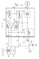
- Fig. 1 is a block diagram illustrating an electronic apparatus according to a first exemplary embodiment of the present invention.
- the electronic apparatus is a recording apparatus which applies signals (scan signals) to a recording head to execute recording on a recoding medium.
- An integrated circuit 104 includes a driving circuit for driving a load (for example, motor).
- a power source 101 is an alternating current/ direct current (AC/DC) power source.
- the power source 101 receives input from an AC power source 102, thereby outputting a DC voltage 103.
- a voltage (for example, 32 volts (V)) 103 for use in motor driving or the like is output from the power source 101 and input via an input unit (first input unit) 10 of the integrated circuit 104.
- the integrated circuit 104 includes an input unit (second input unit) 11 configured to input a voltage (5 volts) from a smoothing circuit 121 which will be described later.
- the integrated circuit 104 communicates with a CPU 113 using a signal line 122.
- the CPU 113 controls operation of a recording apparatus.
- the integrated circuit 104 includes a regulator 106, a controller 107, a motor driver 108, and a switching circuit 109.
- the integrated circuit 104 further includes a switch 105.
- the regulator (voltage conversion circuit) 106 decreases an input voltage to a predetermined voltage.
- the switch 105 selects an electric power source supplied to the regulator 106. With the switch 105, it is determined whether electric power is supplied from the input unit 10 or the input unit 11. For example, when the integrated circuit 104 is started, electric power input from the input unit 10 is supplied to the regulator 106. Then, once a predetermined condition is met, electric power input from the input unit 11 is supplied to the regulator 106.
- the controller 107 operates at a voltage of 3.3 volts generated by the regulator 106.
- the controller 107 controls the motor driver 108 and the switching circuit 109.
- the controller 107 controls the motor driver 108 and the switching circuit 109 based on commands and data input from an input and output unit 17. Further, the controller 107 outputs information concerning a state of an integrated circuit or the like from the input and output unit 17 to a CPU.
- a capacitor 110 is connected to an output of the regulator 106 via an external terminal for the purpose of stabilizing a voltage.
- the switching circuit 109 has two outputs 13 and 14. A switching element (for example, field effect transistor (FET)) within the switching circuit 109 is associated with each of these outputs.
- the IC controller 107 includes two control circuits, each of which controls one of the switching elements in the switching circuit 109.
- the switching circuit 109 cooperates with the smoothing circuit 121 to generate two different power supply voltages (voltage pulse signals) Va and Vb. One of these power supply voltages Va is used to power the CPU 113 and other components (not shown) connected to a power supply line 114.
- the CPU 113 and other components connected to the power supply line 114 can be considered to be a first system.
- the other of the power supply voltages Vb is used to power logic circuits 116 connected to another power supply line 115 and also as the reduced power source voltage for the regulator 106 when the switch 105 is switched over by the CPU.
- the logic circuits 116 and other elements connected to the power supply line 115 can be considered to be a second system.
- the smoothing circuit 121 including inductors (111-a, 111-b) and capacitors (112-a, 112-b), smoothes an output voltage of each output 13 and 14 to convert the voltage into a DC voltage of a desired voltage value.
- a voltage (Va) of the power source line 114 is 1.6 volts and is supplied to the CPU 113.
- a voltage (Vb) of the power source line 115 is 5 volts and is supplied to a logic circuit 116.
- a voltage from the logic circuit 116 is supplied to an operational amplifier provided on a recording head.
- a voltage of the power source line 115 is supplied to the switch 105 provided in the integrated circuit 104 via the input unit 11.
- a voltage divided by resistances 117 and 118 is input as a monitoring signal to a port of the CPU 113 via a power source line 119.
- the CPU 113 determines whether output 115 is normal (suitable for use as a power source for the regulator 106) based on a voltage level input to the port. In this embodiment the CPU 113 determines that the output 115 is normal or suitable when the input voltage level at the port connected to line 119 reaches a predetermined level but in other embodiments the determination could be based on stability of the output 115 or some other relevant criteria.
- the suitability of the output 115 is judged by the CPU 113 indirectly, based on the monitoring signal on line 119, which is possible because the output 119 is dependent on the output 115 as a result of the voltage divider formed by the resistances 117 and 118.
- the suitability could be judged based on the output 115 directly.
- the CPU 113 determines that the output 115 is normal, the CPU 113 outputs a control signal 120 for switching to the switch 105.
- the integrated circuit 104 includes an input unit 12 configured to input the control signal 120.
- the switch 105 switches an electric power supply line to the regulator 106 from the DC voltage 103 to the power source line 115.
- the switch 105 can change an input voltage into the regulator 106 from 32 volts to 5 volts. Subsequently, the regulator 106 decreases a voltage of 5 volts. Control of a motor 122 is executed according to a command from the CPU 113.
- the CPU 113 may confirm a state of a voltage of the power source line 115 by confirming normal activation of the switching element 109.
- the resistances 117 and 118 become unnecessary, and a port do not need to be allocated to the CPU 113.
- a reduction in resistance element and allocation of a port to other applications can be achieved.
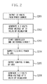
- Fig. 2 is a flowchart illustrating operation of an electronic apparatus according to the first exemplary embodiment.
- the power source 101 outputs a direct current voltage of 32 volts.
- the regulator 106 generates a voltage of 3.3 volts.
- the controller 107 and the switching circuit 109 start operating. When the switching circuit 109 starts operation, a voltage is generated in the smoothing circuit 121.
- the CPU 113 receives the power supply voltage Va from the smoothing circuit 121 and is activated. After the CPU 113 is activated, the CPU 113 compares output 119 of the smoothing circuit 121 and a threshold voltage, thereby confirming that the switching circuit 109 and the smoothing circuit 121 are operating normally.
- step S205 the CPU 113 outputs the control signal 120 to the integrated circuit 104.
- step S206 when the control signal 120 is input, the switch 105 is operated and the regulator 106 generates a voltage of 3.3 volts from a voltage of 5 volts. Subsequently, the regulator 106 continues to generate a voltage of 3.3 volts from a voltage of 5 volts.
- a relation between electric power and heat generation is as follows. Output of the power source 103 is 32 V (volts), a voltage generated in the smoothing circuit 121 and input to the integrated circuit 104 is 5 V (volts), and a voltage generated by the regulator is 3.3 V (volts). A heat resistance is 25° C /W with an integrated circuit mounted on a substrate and a logic current consumed when an integrated circuit is operated is 20 mA.
- Fig. 3 is a block diagram illustrating an electronic apparatus according to a second exemplary embodiment of the present invention. Only points different from the first exemplary embodiment will be described. In the second exemplary embodiment, with respect to points similar to the first exemplary embodiments, descriptions will be omitted.
- the operation of a switch 305 has been executed based on a signal from the CPU 113 outside an integrated circuit. However, in the second exemplary embodiment, the operation of the switch 305 is executed by a switch controller 315.
- the switch controller 315 receives the power supply it needs for its operation from a regulator 306.
- a DC voltage 303 is subjected to pulse control by a switching element and is output.
- This pulse is smoothed by a smoothing circuit including an inductor 311 and a capacitor 312, and is converted into a DC voltage.
- This DC voltage is supplied to a CPU 313 via a power source line 314. Further, this DC voltage is input from an input unit 31 to the switch 305 and the switch controller 315 in the integrated circuit 104.
- Fig. 4 is a flowchart illustrating operation of an electronic apparatus according to the second exemplary embodiment. Since processing from step S401 to step S403 is similar to that in Fig. 2 described in the first exemplary embodiment, their descriptions will be omitted.
- step S404 the switch controller 315 is activated by receiving power supply from the smoothing circuit 321.
- step S405 the switch controller 315 outputs a control signal 320.
- step S406 the switch is operated by the control signal 320 and the regulator 306 generates a voltage of 3.3 volts from a voltage of 5 volts.
- a driving circuit provided in an integrated circuit is not limited to that used for a motor.
- a driving circuit for driving a recording head, a charge coupled device (CCD), a light emitting diode (LED) or the like as a load may be employed.
- the switch controller 315 may be configured to check a voltage input from the input unit 31 using an upper limit voltage value, a lower limit voltage value, or both. When an input voltage is in an abnormal condition, the switch controller 315 may inform the CPU 313 of the abnormal condition.
- the switch controller 315 may execute processing whether an electrical potential of the input unit 31 is 0 V.
- an integrated circuit includes one motor driver circuit.
- an integrated circuit may include a plurality of motor driver circuits.
- An embodiment of the present invention can provide an integrated circuit 104 including a driving circuit for driving a load with a DC voltage generated by a power source circuit and a voltage conversion circuit 106 for decreasing the DC voltage, the integrated circuit 104 comprising: a switching circuit 109 for generating a voltage pulse using the DC voltage; an output unit configured to output the voltage pulse generated by the switching circuit 109 to a smoothing circuit provided outside the integrated circuit 104; a first input unit configured to receive a first DC voltage generated by the power source circuit; a second input unit configured to receive a second DC voltage which is generated by the smoothing circuit and is lower than the first DC voltage; and a control circuit 107 configured to operate based on a voltage decreased by the voltage conversion circuit 106, and control the switching circuit 109 and the driving circuit.
- the integrated circuit 104 may further comprise: a switch circuit configured to perform switching to supply a voltage input from the first input unit to the voltage conversion circuit 106 and supply a voltage input from the second input unit to the voltage conversion circuit 106 after the second DC voltage reaches a predetermined voltage value.
- the switch circuit executes the switching based on a signal output from a second control circuit 107 that is operated based on electric power supplied from the smoothing circuit.
- the load is a motor
- the integrated circuit 104 is a semiconductor circuit of one chip.
- Another embodiment of the present invention can provide an electronic apparatus comprising: an integrated circuit 104 as described above.
- the electronic apparatus may be a recording apparatus.
Landscapes
- Engineering & Computer Science (AREA)
- Power Engineering (AREA)
- Dc-Dc Converters (AREA)
- Control Of Voltage And Current In General (AREA)
Applications Claiming Priority (1)
| Application Number | Priority Date | Filing Date | Title |
|---|---|---|---|
| JP2008134320A JP5247240B2 (ja) | 2008-05-22 | 2008-05-22 | 集積回路、集積回路を備える電子機器 |
Publications (3)
| Publication Number | Publication Date |
|---|---|
| EP2136461A2 true EP2136461A2 (fr) | 2009-12-23 |
| EP2136461A3 EP2136461A3 (fr) | 2017-12-27 |
| EP2136461B1 EP2136461B1 (fr) | 2019-04-24 |
Family
ID=41278119
Family Applications (1)
| Application Number | Title | Priority Date | Filing Date |
|---|---|---|---|
| EP09160904.0A Not-in-force EP2136461B1 (fr) | 2008-05-22 | 2009-05-22 | Circuit de commande et circuit intégré à utiliser avec celui-ci |
Country Status (5)
| Country | Link |
|---|---|
| US (1) | US8487596B2 (fr) |
| EP (1) | EP2136461B1 (fr) |
| JP (1) | JP5247240B2 (fr) |
| KR (1) | KR101154794B1 (fr) |
| CN (2) | CN102664518B (fr) |
Cited By (1)
| Publication number | Priority date | Publication date | Assignee | Title |
|---|---|---|---|---|
| WO2014198309A1 (fr) * | 2013-06-12 | 2014-12-18 | Telefonaktiebolaget L M Ericsson (Publ) | Convertisseur de tension programmable |
Families Citing this family (5)
| Publication number | Priority date | Publication date | Assignee | Title |
|---|---|---|---|---|
| CN102545873B (zh) * | 2010-12-24 | 2013-10-02 | 北京旋极信息技术股份有限公司 | 电平转换系统 |
| CN102857097B (zh) * | 2011-06-30 | 2019-05-17 | 意法半导体研发(深圳)有限公司 | 高效率升压转换器 |
| US9917588B2 (en) * | 2015-07-08 | 2018-03-13 | Nxp B.V. | Level shifter and approach therefor |
| JP6724480B2 (ja) * | 2016-03-30 | 2020-07-15 | ブラザー工業株式会社 | 印刷装置 |
| JP7283239B2 (ja) * | 2019-06-07 | 2023-05-30 | セイコーエプソン株式会社 | 印刷装置 |
Citations (1)
| Publication number | Priority date | Publication date | Assignee | Title |
|---|---|---|---|---|
| JP2006020459A (ja) | 2004-07-02 | 2006-01-19 | Asmo Co Ltd | ステータコア及びこれを備えた回転電機 |
Family Cites Families (18)
| Publication number | Priority date | Publication date | Assignee | Title |
|---|---|---|---|---|
| US4730122A (en) * | 1986-09-18 | 1988-03-08 | International Business Machines Corporation | Power supply adapter systems |
| DE3830016A1 (de) * | 1988-01-29 | 1989-08-10 | Philips Patentverwaltung | Schaltungsanordnung zu speisung einer last |
| JPH0730391A (ja) | 1993-07-08 | 1995-01-31 | Fuji Electric Co Ltd | ドライブ回路 |
| US5528132A (en) * | 1994-02-25 | 1996-06-18 | Maxim Integrated Products | Method and apparatus for increasing switching regulator light load efficiency |
| JP3100914B2 (ja) * | 1996-12-25 | 2000-10-23 | 松下電器産業株式会社 | スイッチング電源 |
| US5945820A (en) * | 1997-02-06 | 1999-08-31 | The Board Of Trustees Of The Leland Stanford Junior University | DC-DC switching regulator with switching rate control |
| JP3469131B2 (ja) * | 1999-07-09 | 2003-11-25 | シャープ株式会社 | 直流安定化電源装置 |
| KR20050090824A (ko) | 2004-03-10 | 2005-09-14 | 삼성전자주식회사 | 동작상태에 따라 상이한 구동전압을 사용하는 전자기기 및그 방법 |
| JP2005323413A (ja) * | 2004-05-06 | 2005-11-17 | Rohm Co Ltd | 過電流検出回路及びこれを有する電源装置 |
| US7429836B2 (en) * | 2004-06-03 | 2008-09-30 | Canon Kabushiki Kaisha | Motor driver circuit, control method thereof, and electronic apparatus |
| JP4612867B2 (ja) * | 2004-06-03 | 2011-01-12 | キヤノン株式会社 | 電力供給回路、モータドライバ回路、電子機器、及び記録装置 |
| JP4502378B2 (ja) * | 2004-07-02 | 2010-07-14 | ローム株式会社 | Dc/dcコンバータ |
| JP4498851B2 (ja) * | 2004-08-11 | 2010-07-07 | ローム株式会社 | 電源装置 |
| JP4439443B2 (ja) * | 2005-07-08 | 2010-03-24 | 富士通株式会社 | 直流電圧変換機能を含む電子機器、および直流電圧変換回路 |
| CN100461594C (zh) * | 2005-07-12 | 2009-02-11 | 中国船舶重工集团公司第七〇九研究所 | 直流电源稳压变换器 |
| JP2008035688A (ja) * | 2006-06-26 | 2008-02-14 | Sanyo Electric Co Ltd | 電動機の駆動装置 |
| CN100556730C (zh) * | 2006-06-30 | 2009-11-04 | 比亚迪股份有限公司 | 混合动力汽车的直流电压控制系统及其工作方法 |
| US7795848B2 (en) * | 2007-05-09 | 2010-09-14 | Freescale Semiconductor, Inc. | Method and circuit for generating output voltages from input voltage |
-
2008
- 2008-05-22 JP JP2008134320A patent/JP5247240B2/ja not_active Expired - Fee Related
-
2009
- 2009-05-21 US US12/470,395 patent/US8487596B2/en active Active
- 2009-05-22 CN CN201210132113.8A patent/CN102664518B/zh not_active Expired - Fee Related
- 2009-05-22 EP EP09160904.0A patent/EP2136461B1/fr not_active Not-in-force
- 2009-05-22 KR KR1020090045044A patent/KR101154794B1/ko not_active Expired - Fee Related
- 2009-05-22 CN CN2009102029554A patent/CN101588174B/zh not_active Expired - Fee Related
Patent Citations (1)
| Publication number | Priority date | Publication date | Assignee | Title |
|---|---|---|---|---|
| JP2006020459A (ja) | 2004-07-02 | 2006-01-19 | Asmo Co Ltd | ステータコア及びこれを備えた回転電機 |
Cited By (1)
| Publication number | Priority date | Publication date | Assignee | Title |
|---|---|---|---|---|
| WO2014198309A1 (fr) * | 2013-06-12 | 2014-12-18 | Telefonaktiebolaget L M Ericsson (Publ) | Convertisseur de tension programmable |
Also Published As
| Publication number | Publication date |
|---|---|
| JP5247240B2 (ja) | 2013-07-24 |
| JP2009282764A (ja) | 2009-12-03 |
| CN102664518B (zh) | 2014-10-15 |
| EP2136461B1 (fr) | 2019-04-24 |
| US8487596B2 (en) | 2013-07-16 |
| KR101154794B1 (ko) | 2012-06-18 |
| CN101588174A (zh) | 2009-11-25 |
| CN101588174B (zh) | 2012-06-20 |
| EP2136461A3 (fr) | 2017-12-27 |
| KR20090122150A (ko) | 2009-11-26 |
| CN102664518A (zh) | 2012-09-12 |
| US20090289613A1 (en) | 2009-11-26 |
Similar Documents
| Publication | Publication Date | Title |
|---|---|---|
| JP4431405B2 (ja) | 低コストdc−dc電圧スイッチングコンバータレギュレータ装置 | |
| JP3722810B2 (ja) | モータ駆動装置 | |
| CN100550588C (zh) | 电源电路、电源控制电路和电源控制方法 | |
| JP5157603B2 (ja) | 昇圧型dc−dcコンバータおよび電源駆動用半導体集積回路 | |
| CN107820664B (zh) | 驱动装置 | |
| EP2136461B1 (fr) | Circuit de commande et circuit intégré à utiliser avec celui-ci | |
| EP1411406B1 (fr) | Alimentations électriques multiples | |
| CN100463343C (zh) | 电源装置 | |
| CN1996732A (zh) | 开关电源装置和用于该开关电源装置的半导体装置 | |
| JP6162445B2 (ja) | 電力変換装置 | |
| JP7063297B2 (ja) | 車載電源装置 | |
| CN104350671B (zh) | 开关转换电源装置 | |
| JP2012205408A (ja) | 電源回路 | |
| JP2010074891A (ja) | 半導体回路 | |
| CN107885154B (zh) | 可编程逻辑控制器 | |
| JP5181959B2 (ja) | 直流電源装置および電源制御用半導体集積回路 | |
| JP2009240112A (ja) | 電源装置および半導体集積回路装置 | |
| JP4282673B2 (ja) | スイッチング電源装置 | |
| JP4983275B2 (ja) | Dc/dcコンバータ | |
| CN105940598A (zh) | 电源装置 | |
| JP3661472B2 (ja) | 電源装置 | |
| JP2016158071A (ja) | 電流制御装置及び電源システム | |
| KR100715773B1 (ko) | 제어용 전원을 공급하기 위한 전원 공급 장치 | |
| JP4778870B2 (ja) | 負電源回路を有する電源装置 | |
| JP4690213B2 (ja) | Dc/dcコンバータ |
Legal Events
| Date | Code | Title | Description |
|---|---|---|---|
| PUAI | Public reference made under article 153(3) epc to a published international application that has entered the european phase |
Free format text: ORIGINAL CODE: 0009012 |
|
| AK | Designated contracting states |
Kind code of ref document: A2 Designated state(s): AT BE BG CH CY CZ DE DK EE ES FI FR GB GR HR HU IE IS IT LI LT LU LV MC MK MT NL NO PL PT RO SE SI SK TR |
|
| PUAL | Search report despatched |
Free format text: ORIGINAL CODE: 0009013 |
|
| AK | Designated contracting states |
Kind code of ref document: A3 Designated state(s): AT BE BG CH CY CZ DE DK EE ES FI FR GB GR HR HU IE IS IT LI LT LU LV MC MK MT NL NO PL PT RO SE SI SK TR |
|
| AX | Request for extension of the european patent |
Extension state: AL BA RS |
|
| RIC1 | Information provided on ipc code assigned before grant |
Ipc: H02M 7/48 20070101ALI20171121BHEP Ipc: H02M 1/36 20070101ALI20171121BHEP Ipc: H02M 3/155 20060101AFI20171121BHEP |
|
| STAA | Information on the status of an ep patent application or granted ep patent |
Free format text: STATUS: REQUEST FOR EXAMINATION WAS MADE |
|
| 17P | Request for examination filed |
Effective date: 20180627 |
|
| RBV | Designated contracting states (corrected) |
Designated state(s): AT BE BG CH CY CZ DE DK EE ES FI FR GB GR HR HU IE IS IT LI LT LU LV MC MK MT NL NO PL PT RO SE SI SK TR |
|
| GRAP | Despatch of communication of intention to grant a patent |
Free format text: ORIGINAL CODE: EPIDOSNIGR1 |
|
| STAA | Information on the status of an ep patent application or granted ep patent |
Free format text: STATUS: GRANT OF PATENT IS INTENDED |
|
| RIC1 | Information provided on ipc code assigned before grant |
Ipc: H02M 3/155 20060101AFI20181004BHEP Ipc: H02M 1/36 20070101ALI20181004BHEP Ipc: H02M 7/48 20070101ALI20181004BHEP |
|
| INTG | Intention to grant announced |
Effective date: 20181102 |
|
| GRAS | Grant fee paid |
Free format text: ORIGINAL CODE: EPIDOSNIGR3 |
|
| GRAA | (expected) grant |
Free format text: ORIGINAL CODE: 0009210 |
|
| STAA | Information on the status of an ep patent application or granted ep patent |
Free format text: STATUS: THE PATENT HAS BEEN GRANTED |
|
| AK | Designated contracting states |
Kind code of ref document: B1 Designated state(s): AT BE BG CH CY CZ DE DK EE ES FI FR GB GR HR HU IE IS IT LI LT LU LV MC MK MT NL NO PL PT RO SE SI SK TR |
|
| REG | Reference to a national code |
Ref country code: GB Ref legal event code: FG4D |
|
| REG | Reference to a national code |
Ref country code: CH Ref legal event code: EP |
|
| REG | Reference to a national code |
Ref country code: AT Ref legal event code: REF Ref document number: 1125307 Country of ref document: AT Kind code of ref document: T Effective date: 20190515 Ref country code: IE Ref legal event code: FG4D |
|
| REG | Reference to a national code |
Ref country code: DE Ref legal event code: R096 Ref document number: 602009057993 Country of ref document: DE |
|
| REG | Reference to a national code |
Ref country code: NL Ref legal event code: MP Effective date: 20190424 |
|
| REG | Reference to a national code |
Ref country code: LT Ref legal event code: MG4D |
|
| PG25 | Lapsed in a contracting state [announced via postgrant information from national office to epo] |
Ref country code: NL Free format text: LAPSE BECAUSE OF FAILURE TO SUBMIT A TRANSLATION OF THE DESCRIPTION OR TO PAY THE FEE WITHIN THE PRESCRIBED TIME-LIMIT Effective date: 20190424 |
|
| PG25 | Lapsed in a contracting state [announced via postgrant information from national office to epo] |
Ref country code: FI Free format text: LAPSE BECAUSE OF FAILURE TO SUBMIT A TRANSLATION OF THE DESCRIPTION OR TO PAY THE FEE WITHIN THE PRESCRIBED TIME-LIMIT Effective date: 20190424 Ref country code: NO Free format text: LAPSE BECAUSE OF FAILURE TO SUBMIT A TRANSLATION OF THE DESCRIPTION OR TO PAY THE FEE WITHIN THE PRESCRIBED TIME-LIMIT Effective date: 20190724 Ref country code: PT Free format text: LAPSE BECAUSE OF FAILURE TO SUBMIT A TRANSLATION OF THE DESCRIPTION OR TO PAY THE FEE WITHIN THE PRESCRIBED TIME-LIMIT Effective date: 20190824 Ref country code: HR Free format text: LAPSE BECAUSE OF FAILURE TO SUBMIT A TRANSLATION OF THE DESCRIPTION OR TO PAY THE FEE WITHIN THE PRESCRIBED TIME-LIMIT Effective date: 20190424 Ref country code: SE Free format text: LAPSE BECAUSE OF FAILURE TO SUBMIT A TRANSLATION OF THE DESCRIPTION OR TO PAY THE FEE WITHIN THE PRESCRIBED TIME-LIMIT Effective date: 20190424 Ref country code: LT Free format text: LAPSE BECAUSE OF FAILURE TO SUBMIT A TRANSLATION OF THE DESCRIPTION OR TO PAY THE FEE WITHIN THE PRESCRIBED TIME-LIMIT Effective date: 20190424 Ref country code: ES Free format text: LAPSE BECAUSE OF FAILURE TO SUBMIT A TRANSLATION OF THE DESCRIPTION OR TO PAY THE FEE WITHIN THE PRESCRIBED TIME-LIMIT Effective date: 20190424 |
|
| PG25 | Lapsed in a contracting state [announced via postgrant information from national office to epo] |
Ref country code: LV Free format text: LAPSE BECAUSE OF FAILURE TO SUBMIT A TRANSLATION OF THE DESCRIPTION OR TO PAY THE FEE WITHIN THE PRESCRIBED TIME-LIMIT Effective date: 20190424 Ref country code: BG Free format text: LAPSE BECAUSE OF FAILURE TO SUBMIT A TRANSLATION OF THE DESCRIPTION OR TO PAY THE FEE WITHIN THE PRESCRIBED TIME-LIMIT Effective date: 20190724 Ref country code: GR Free format text: LAPSE BECAUSE OF FAILURE TO SUBMIT A TRANSLATION OF THE DESCRIPTION OR TO PAY THE FEE WITHIN THE PRESCRIBED TIME-LIMIT Effective date: 20190725 Ref country code: PL Free format text: LAPSE BECAUSE OF FAILURE TO SUBMIT A TRANSLATION OF THE DESCRIPTION OR TO PAY THE FEE WITHIN THE PRESCRIBED TIME-LIMIT Effective date: 20190424 |
|
| REG | Reference to a national code |
Ref country code: AT Ref legal event code: MK05 Ref document number: 1125307 Country of ref document: AT Kind code of ref document: T Effective date: 20190424 |
|
| REG | Reference to a national code |
Ref country code: CH Ref legal event code: PL |
|
| PG25 | Lapsed in a contracting state [announced via postgrant information from national office to epo] |
Ref country code: IS Free format text: LAPSE BECAUSE OF FAILURE TO SUBMIT A TRANSLATION OF THE DESCRIPTION OR TO PAY THE FEE WITHIN THE PRESCRIBED TIME-LIMIT Effective date: 20190824 |
|
| REG | Reference to a national code |
Ref country code: DE Ref legal event code: R097 Ref document number: 602009057993 Country of ref document: DE |
|
| PG25 | Lapsed in a contracting state [announced via postgrant information from national office to epo] |
Ref country code: CZ Free format text: LAPSE BECAUSE OF FAILURE TO SUBMIT A TRANSLATION OF THE DESCRIPTION OR TO PAY THE FEE WITHIN THE PRESCRIBED TIME-LIMIT Effective date: 20190424 Ref country code: LI Free format text: LAPSE BECAUSE OF NON-PAYMENT OF DUE FEES Effective date: 20190531 Ref country code: CH Free format text: LAPSE BECAUSE OF NON-PAYMENT OF DUE FEES Effective date: 20190531 Ref country code: MC Free format text: LAPSE BECAUSE OF FAILURE TO SUBMIT A TRANSLATION OF THE DESCRIPTION OR TO PAY THE FEE WITHIN THE PRESCRIBED TIME-LIMIT Effective date: 20190424 Ref country code: SK Free format text: LAPSE BECAUSE OF FAILURE TO SUBMIT A TRANSLATION OF THE DESCRIPTION OR TO PAY THE FEE WITHIN THE PRESCRIBED TIME-LIMIT Effective date: 20190424 Ref country code: DK Free format text: LAPSE BECAUSE OF FAILURE TO SUBMIT A TRANSLATION OF THE DESCRIPTION OR TO PAY THE FEE WITHIN THE PRESCRIBED TIME-LIMIT Effective date: 20190424 Ref country code: EE Free format text: LAPSE BECAUSE OF FAILURE TO SUBMIT A TRANSLATION OF THE DESCRIPTION OR TO PAY THE FEE WITHIN THE PRESCRIBED TIME-LIMIT Effective date: 20190424 Ref country code: AT Free format text: LAPSE BECAUSE OF FAILURE TO SUBMIT A TRANSLATION OF THE DESCRIPTION OR TO PAY THE FEE WITHIN THE PRESCRIBED TIME-LIMIT Effective date: 20190424 Ref country code: RO Free format text: LAPSE BECAUSE OF FAILURE TO SUBMIT A TRANSLATION OF THE DESCRIPTION OR TO PAY THE FEE WITHIN THE PRESCRIBED TIME-LIMIT Effective date: 20190424 |
|
| REG | Reference to a national code |
Ref country code: BE Ref legal event code: MM Effective date: 20190531 |
|
| PG25 | Lapsed in a contracting state [announced via postgrant information from national office to epo] |
Ref country code: LU Free format text: LAPSE BECAUSE OF NON-PAYMENT OF DUE FEES Effective date: 20190522 Ref country code: IT Free format text: LAPSE BECAUSE OF FAILURE TO SUBMIT A TRANSLATION OF THE DESCRIPTION OR TO PAY THE FEE WITHIN THE PRESCRIBED TIME-LIMIT Effective date: 20190424 |
|
| PLBE | No opposition filed within time limit |
Free format text: ORIGINAL CODE: 0009261 |
|
| STAA | Information on the status of an ep patent application or granted ep patent |
Free format text: STATUS: NO OPPOSITION FILED WITHIN TIME LIMIT |
|
| GBPC | Gb: european patent ceased through non-payment of renewal fee |
Effective date: 20190724 |
|
| PG25 | Lapsed in a contracting state [announced via postgrant information from national office to epo] |
Ref country code: TR Free format text: LAPSE BECAUSE OF FAILURE TO SUBMIT A TRANSLATION OF THE DESCRIPTION OR TO PAY THE FEE WITHIN THE PRESCRIBED TIME-LIMIT Effective date: 20190424 |
|
| 26N | No opposition filed |
Effective date: 20200127 |
|
| PG25 | Lapsed in a contracting state [announced via postgrant information from national office to epo] |
Ref country code: GB Free format text: LAPSE BECAUSE OF NON-PAYMENT OF DUE FEES Effective date: 20190724 Ref country code: IE Free format text: LAPSE BECAUSE OF NON-PAYMENT OF DUE FEES Effective date: 20190522 |
|
| PG25 | Lapsed in a contracting state [announced via postgrant information from national office to epo] |
Ref country code: SI Free format text: LAPSE BECAUSE OF FAILURE TO SUBMIT A TRANSLATION OF THE DESCRIPTION OR TO PAY THE FEE WITHIN THE PRESCRIBED TIME-LIMIT Effective date: 20190424 Ref country code: BE Free format text: LAPSE BECAUSE OF NON-PAYMENT OF DUE FEES Effective date: 20190531 |
|
| PG25 | Lapsed in a contracting state [announced via postgrant information from national office to epo] |
Ref country code: FR Free format text: LAPSE BECAUSE OF NON-PAYMENT OF DUE FEES Effective date: 20190624 |
|
| PG25 | Lapsed in a contracting state [announced via postgrant information from national office to epo] |
Ref country code: CY Free format text: LAPSE BECAUSE OF FAILURE TO SUBMIT A TRANSLATION OF THE DESCRIPTION OR TO PAY THE FEE WITHIN THE PRESCRIBED TIME-LIMIT Effective date: 20190424 |
|
| PG25 | Lapsed in a contracting state [announced via postgrant information from national office to epo] |
Ref country code: HU Free format text: LAPSE BECAUSE OF FAILURE TO SUBMIT A TRANSLATION OF THE DESCRIPTION OR TO PAY THE FEE WITHIN THE PRESCRIBED TIME-LIMIT; INVALID AB INITIO Effective date: 20090522 Ref country code: MT Free format text: LAPSE BECAUSE OF FAILURE TO SUBMIT A TRANSLATION OF THE DESCRIPTION OR TO PAY THE FEE WITHIN THE PRESCRIBED TIME-LIMIT Effective date: 20190424 |
|
| PG25 | Lapsed in a contracting state [announced via postgrant information from national office to epo] |
Ref country code: MK Free format text: LAPSE BECAUSE OF FAILURE TO SUBMIT A TRANSLATION OF THE DESCRIPTION OR TO PAY THE FEE WITHIN THE PRESCRIBED TIME-LIMIT Effective date: 20190424 |
|
| PGFP | Annual fee paid to national office [announced via postgrant information from national office to epo] |
Ref country code: DE Payment date: 20230419 Year of fee payment: 15 |
|
| REG | Reference to a national code |
Ref country code: DE Ref legal event code: R119 Ref document number: 602009057993 Country of ref document: DE |
|
| PG25 | Lapsed in a contracting state [announced via postgrant information from national office to epo] |
Ref country code: DE Free format text: LAPSE BECAUSE OF NON-PAYMENT OF DUE FEES Effective date: 20241203 |