EP2137734B1 - Magnetoresistiver stt-ram und entwurfsverfahren - Google Patents
Magnetoresistiver stt-ram und entwurfsverfahren Download PDFInfo
- Publication number
- EP2137734B1 EP2137734B1 EP08745261A EP08745261A EP2137734B1 EP 2137734 B1 EP2137734 B1 EP 2137734B1 EP 08745261 A EP08745261 A EP 08745261A EP 08745261 A EP08745261 A EP 08745261A EP 2137734 B1 EP2137734 B1 EP 2137734B1
- Authority
- EP
- European Patent Office
- Prior art keywords
- voltage
- read
- write
- mtj
- resistance
- Prior art date
- Legal status (The legal status is an assumption and is not a legal conclusion. Google has not performed a legal analysis and makes no representation as to the accuracy of the status listed.)
- Active
Links
Images




Classifications
-
- G—PHYSICS
- G11—INFORMATION STORAGE
- G11C—STATIC STORES
- G11C11/00—Digital stores characterised by the use of particular electric or magnetic storage elements; Storage elements therefor
- G11C11/02—Digital stores characterised by the use of particular electric or magnetic storage elements; Storage elements therefor using magnetic elements
- G11C11/16—Digital stores characterised by the use of particular electric or magnetic storage elements; Storage elements therefor using magnetic elements using elements in which the storage effect is based on magnetic spin effect
-
- G—PHYSICS
- G11—INFORMATION STORAGE
- G11C—STATIC STORES
- G11C11/00—Digital stores characterised by the use of particular electric or magnetic storage elements; Storage elements therefor
- G11C11/02—Digital stores characterised by the use of particular electric or magnetic storage elements; Storage elements therefor using magnetic elements
- G11C11/14—Digital stores characterised by the use of particular electric or magnetic storage elements; Storage elements therefor using magnetic elements using thin-film elements
- G11C11/15—Digital stores characterised by the use of particular electric or magnetic storage elements; Storage elements therefor using magnetic elements using thin-film elements using multiple magnetic layers
-
- G—PHYSICS
- G11—INFORMATION STORAGE
- G11C—STATIC STORES
- G11C11/00—Digital stores characterised by the use of particular electric or magnetic storage elements; Storage elements therefor
- G11C11/02—Digital stores characterised by the use of particular electric or magnetic storage elements; Storage elements therefor using magnetic elements
- G11C11/16—Digital stores characterised by the use of particular electric or magnetic storage elements; Storage elements therefor using magnetic elements using elements in which the storage effect is based on magnetic spin effect
- G11C11/165—Auxiliary circuits
- G11C11/1659—Cell access
-
- G—PHYSICS
- G11—INFORMATION STORAGE
- G11C—STATIC STORES
- G11C11/00—Digital stores characterised by the use of particular electric or magnetic storage elements; Storage elements therefor
- G11C11/02—Digital stores characterised by the use of particular electric or magnetic storage elements; Storage elements therefor using magnetic elements
- G11C11/16—Digital stores characterised by the use of particular electric or magnetic storage elements; Storage elements therefor using magnetic elements using elements in which the storage effect is based on magnetic spin effect
- G11C11/165—Auxiliary circuits
- G11C11/1673—Reading or sensing circuits or methods
-
- G—PHYSICS
- G11—INFORMATION STORAGE
- G11C—STATIC STORES
- G11C11/00—Digital stores characterised by the use of particular electric or magnetic storage elements; Storage elements therefor
- G11C11/02—Digital stores characterised by the use of particular electric or magnetic storage elements; Storage elements therefor using magnetic elements
- G11C11/16—Digital stores characterised by the use of particular electric or magnetic storage elements; Storage elements therefor using magnetic elements using elements in which the storage effect is based on magnetic spin effect
- G11C11/165—Auxiliary circuits
- G11C11/1675—Writing or programming circuits or methods
-
- H—ELECTRICITY
- H10—SEMICONDUCTOR DEVICES; ELECTRIC SOLID-STATE DEVICES NOT OTHERWISE PROVIDED FOR
- H10B—ELECTRONIC MEMORY DEVICES
- H10B61/00—Magnetic memory devices, e.g. magnetoresistive RAM [MRAM] devices
- H10B61/20—Magnetic memory devices, e.g. magnetoresistive RAM [MRAM] devices comprising components having three or more electrodes, e.g. transistors
- H10B61/22—Magnetic memory devices, e.g. magnetoresistive RAM [MRAM] devices comprising components having three or more electrodes, e.g. transistors of the field-effect transistor [FET] type
-
- H—ELECTRICITY
- H10—SEMICONDUCTOR DEVICES; ELECTRIC SOLID-STATE DEVICES NOT OTHERWISE PROVIDED FOR
- H10N—ELECTRIC SOLID-STATE DEVICES NOT OTHERWISE PROVIDED FOR
- H10N50/00—Galvanomagnetic devices
- H10N50/10—Magnetoresistive devices
Definitions
- Embodiments of the invention are related to random access memory (RAM). More particularly, embodiments of the invention are related to memory design in Spin Transfer Torque Magnetoresistive Random Access Memory (STT-MRAM).
- STT-MRAM Spin Transfer Torque Magnetoresistive Random Access Memory
- RAM Random access memory
- RAM can be stand alone devices or can be integrated or embedded within devices that use the RAM, such as microprocessors, microcontrollers, application specific integrated circuits (ASICs), system-on-chip (SoC), and other like devices as will be appreciated by those skilled in the art.
- RAM can be volatile or non-volatile. Volatile RAM loses its stored information whenever power is removed. Non-volatile RAM can maintain its memory contents even when power is removed from the memory. Although non-volatile RAM has advantages in the ability to maintain its contents without having power applied, conventional non-volatile RAM has slower read / write times than volatile RAM.
- Magnetoresistive Random Access Memory is a non-volatile memory technology that has response (read / write) times comparable to volatile memory. In contrast to conventional RAM technologies which store data as electric charges or current flows. MRAM uses magnetic elements. As illustrated in Figs 1A and 1B , a magnetic tunnel junction (MTJ) storage element 100 can be formed from two magnetic layers 110 and 130, each of which can hold a magnetic field, separated by an insulating (tunnel barrier) layer 120. One of the two layers (e.g., fixed layer 110), is set to a particular polarity. The other layer's (e.g., free layer 130) polarity 132 is free to change to match that of an external field that can be applied.
- MTJ magnetic tunnel junction
- a change in the polarity 132 of the free layer 130 will change the resistance of the MTJ storage element 100.
- Fig. 1A a low resistance state exists.
- Fig. 1B a high resistance state exists.
- the illustration of MTJ 100 has been simplified and those skilled in the art will appreciate that each layer illustrated may comprise one or more layers of materials, as is known in the art.
- a memory cell 200 of a conventional MRAM is illustrated for a read operation.
- the cell 200 includes a transistor 210, bit line 220, digit line 230 and word line 240.
- the cell 200 can be read by measuring the electrical resistance of the MTJ 100.
- a particular MTJ 100 can be selected by activating an associated transistor 210, which can switch current from a bit line 220 through the MTJ 100.
- the electrical resistance of the MTJ 100 changes based on the orientation of the polarities in the two magnetic layers (e.g., 110, 130), as discussed above.
- the resistance inside any particular MTJ 100 can be determined from the current, resulting from the polarity of the free layer. Conventionally, if the fixed layer 110 and free layer 130 have the same polarity, the resistance is low and a "0" is read. If the fixed layer 110 and free layer 130 have opposite polarity, the resistance is higher and a "1" is read.
- the memory cell 200 of a conventional MRAM is illustrated for a write operation.
- the write operation of the MRAM is a magnetic operation. Accordingly, transistor 210 is off during the write operation.
- Current is propagated through the bit line 220 and digit line 230 to establish magnetic fields 250 and 260 that can affect the polarity of the free layer of the MTJ 100 and consequently the logic state of the cell 200. Accordingly, data can be written to and stored in the MTJ 100.
- MRAM has several desirable characteristics that make it a candidate for a universal memory, such as high speed, high density (i.e., small bitcell size), low power consumption, and no degradation over time.
- MRAM has scalability issues. Specifically, as the bit cells become smaller, the magnetic fields used for switching the memory state increase. Accordingly, current density and power consumption increase to provide the higher magnetic fields, thus limiting the scalability of the MRAM.
- STT-MRAM Spin Transfer Torque Magnetoresistive Random Access Memory
- STT-MRAM uses electrons that become spin-polarized as the electrons pass through a thin film (spin filter).
- STT-MRAM is also known as Spin Transfer Torque RAM (STT-RAM), Spin Torque Transfer Magnetization Switching RAM (Spin-RAM), and Spin Momentum Transfer (SMT-RAM).
- STT-RAM Spin Transfer Torque RAM
- Spin-RAM Spin Torque Transfer Magnetization Switching RAM
- SMT-RAM Spin Momentum Transfer
- the read operation is similar to conventional MRAM in that a current is used to detect the resistance / logic state of the MTJ storage element, as discussed in the foregoing. As illustrated in Fig.
- a STT-MRAM bit cell 300 includes MTJ 305, transistor 310, bit line 320 and word line 330.
- the transistor 310 is switched on for both read and write operations to allow current to flow through the MTJ 305, so that the logic state can be read or written.
- FIG. 3B a more detailed diagram of a STT-MRAM cell 301 is illustrated, for further discussion of the read / write operations.
- the write operation in an STT-MRAM is electrical.
- Read / write circuitry 360 generates a write voltage between the bit line 320 and the source line 340.
- the polarity of the free layer of the MTJ 305 can be changed and correspondingly the logic state can be written to the cell 301.
- a read current is generated, which flows between the bit line 320 and source line 340 through MTJ 305.
- the resistance (logic state) of the MTJ 305 can be determined based on the voltage differential between the bit line 320 and source line 340, which is compared to a reference 370 and then amplified by sense amplifier 350.
- STT-MRAM eliminates the scaling problem due to the magnetic write operation in MRAM. Further, the circuit design is less complicated for STT-MRAM. However, because both read and write operations are performed by passing current through the MTJ 305, there is a potential for read operations to disturb the data stored in the MTJ 305. For example, if the read current is similar to or greater in magnitude than the write current threshold, then there is a substantial chance the read operation may disturb the logic state of MTJ 305 and thus degrade the integrity of the memory. [0010a] US 2007/003074 describes a magnetic memory device utilizing spin transfer, wherein the memory cells comprise an access transistor and a MTJ junction. FR2829868 describes a magnetic memory with spin-polarized current writing.
- US6269018 describes a Magnetic random access memory having a first free ferromagnetic layer, a second free ferromagnetic layer extending in a direction parallel to the first ferromagnetic layer, and a highly conductive layer formed between the first ferromagnetic layer and the second ferromagnetic layer.
- Exemplary embodiments of the invention are directed to systems, circuits and methods for a reduced read voltage in a Spin Transfer Torque Magnetoresistive Random Access Memory (STT-MRAM).
- STT-MRAM Spin Transfer Torque Magnetoresistive Random Access Memory
- an embodiment of the invention can include a method for designing Spin Transfer Torque Magnetoresistive Random Access Memory (STT-MRAM) comprising: obtaining a characteristic curve for an access transistor; determining a state0 resistance and a state 1 resistance of a magnetic tunnel junction (MTJ) storage element, corresponding to a first and second state of the memory; determining a write voltage such that the operating points of both the first state and second state write operations intercept the characteristic curve in a saturated region; and determining a read voltage such that the operating points of both the first state and second state read operations intercept the characteristic curve in a linear region.
- STT-MRAM Spin Transfer Torque Magnetoresistive Random Access Memory
- STT-MRAM having a plurality of bit cells, each bit cell comprising: a magnetic tunnel junction (MTJ) storage element having a state0 resistance and a state 1 resistance, corresponding to a first and second state of the memory; an access transistor coupled in series with the MTJ between a bit line and a source line, wherein a gate of the access transistor is coupled to a word line; a supply voltage (VDD) coupled to the bit line or source line during write operations; and a read voltage (VR) coupled to the bit line during a read operation, and wherein the read voltage is selected such that the access transistor operates in a linear region during read operations and wherein the access transistor operates in a saturation region during write operations.
- VDD supply voltage
- VR read voltage
- Another embodiment of the invention includes a computer-readable medium including code stored thereon for designing Spin Transfer Torque Magnetoresistive Random Access Memory (STT-MRAM) comprising: code for causing a computer to load a characteristic curve for an access transistor; code for causing a computer to determine a state0 resistance and a state 1 resistance of a magnetic tunnel junction (MTJ) storage element, corresponding to a first and second state of the memory; code for causing a computer to determine a write voltage such that the operating points of both the first state and second state write operations intercept the characteristic curve in a saturated region; and code for causing a computer to determine a read voltage such that the operating points of both the first state and second state read operations intercept the characteristic curve in a linear region.
- STT-MRAM Spin Transfer Torque Magnetoresistive Random Access Memory
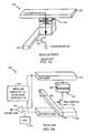
- Figs. 1A and 1B are illustrations of a magnetic tunnel junction (MTJ) storage element.
- MTJ magnetic tunnel junction
- Figs. 2A and 2B are illustrations of a Magnetoresistive Random Access Memory (MRAM) cell during read and write operations, respectively.
- MRAM Magnetoresistive Random Access Memory
- Figs. 3A and 3B are illustrations of Spin Transfer Torque Magnetoresistive Random Access Memory (STT-MRAM) cells.
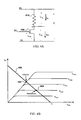
- Fig. 4A is a simplified schematic representation of a STT-MRAM cell.
- Fig. 4B is a graph illustrating characteristic curves for a word line transistor and load line indicating various operating points.
- Fig. 5A is a graph illustrating a characteristic curve for a word line transistor and load lines indicating various read operating points in the saturated region.
- Fig. 5B is a graph illustrating a characteristic curve for a word line transistor and load lines indicating various read operating points in the linear region.
- Fig. 6A is a graph illustrating a characteristic curve for a word line transistor and load lines indicating various write operating points in the saturated region.
- Fig. 6B is a graph illustrating a characteristic curve for a word line transistor and load lines indicating various write operating points in the linear region.
- Fig. 7 is a graph illustrating a characteristic curve for a word line transistor and load lines indicating various read and write operating points.
- Fig. 8 is a graph illustrating a characteristic curve for a word line transistor and load lines indicating various read and write operating points.
- Fig. 9 is a flowchart illustrating a design method to determine various operating points of a STT-MRAM bit cell.
- STT-MRAM uses a low write current for each cell, which is an advantage of this memory type over MRAM.
- cell read current can approach or be higher than the write current threshold and thus cause an invalid write operation / destructive read to occur.
- FIG. 4A a simplified schematic of an STT-MRAM cell is illustrated.
- the MTJ is represented by resistance (R) 410 and is in series with the access transistor 420 between the bit line (BL) and source line (SL).
- the cell operation can be considered to have three modes; Breakdown; Read; and Write.
- a large cell current difference between state0 and state1 is desired for proper sensing operation.
- the Write mode the write operation is a bidirectional operation to write state0 and state1, as previously discussed.
- a low write current is used for low power operation.
- the Breakdown mode can occur if the voltage across the MTJ (e.g., V M ) during a write operation is higher than V breakdown .
- the voltage (V) is the sum of the voltage across the MTJ (V M ) and the drain-source voltage (V DS ).
- I DS drain-source current
- V GS gate-source voltage
- V DS drain-source voltage
- V t transistor threshold voltage
- W/L channel width to channel length ratio
- V GS V WL - V SL ,
- V WL the voltage on the word line
- V SL the voltage on the source line.
- V D is the voltage at node D between the MTJ 410 and the access transistor 420.
- V BL is the voltage on the bit line.
- the conditions for the linear region and saturation region of the access transistor can be defined as: Linear region : V GS - V T > V DS Saturation region : V GS - V T ⁇ V DS
- characteristic curves for the access (or word line) transistor 420 are provided in Fig. 4B .
- the characteristic curves are a family of curves, each of which is a plot of drain-source current (I DS ) versus drain-source voltage (V DS ) for a particular gate-source voltage (V GS) .
- a load line 450 is plotted. Load line 450 intersects the linear region of the characteristic curves at point 452 and a saturation region at point 454, as can be seen from Fig. 4B .
- Fig. 5A illustrates a load line for the read operation of a state0, 520, and a load line for the read operation of a state 1, 510, for a given read voltage V R .
- Load line 520 has a slope of 1/R 0 , where R 0 is the state0 resistance of the MTJ.
- load line 510 has a slope of t/R 1 where R 1 is the state1 resistance of the MTJ.
- Both lines intersect the drain-source voltage (V DS ) line at point V R and intersect the saturated portion of the access transistor curve at points 512 and 522, respectively.
- V DS drain-source voltage
- Fig. 5B illustrates a load line for the read operation of a state0 540 and a load line for the read operation of a state1 530 for a given read voltage V R and a given gate-source voltage (V GS ).
- Load line 540 has a slope of 1/R 0 , where R 0 is the state0 resistance of the MTJ.
- load line 530 also has a slope of 1/R 1 , where R 1 is the state1 resistance of the MTJ. Both lines intersect the drain-source voltage line at point V R .
- the load lines intersect the linear portion of the access transistor curve at points 532 and 542 for R 1 and R 0 , respectively.
- the read current for state0 can be greater than the read current for state1 (i.e.. I 0 > I 1 ), as can be seen from Fig. 5B .
- the design target of having a significant current difference between state0 and state1 can be achieved. Accordingly, the state of the MTJ will be casier to detect based on the different currents and read errors can be reduced. Other factors can also increase the current difference, such as a smaller on-state resistance R on of the word line (or access) transistor. Additionally, the difference between Round R 1 will also tend to increase the current difference during the read operation.
- the write operation can have a similar current magnitude for each state and preferably has as low a write current, as possible reduce power consumption.
- Load lines for the write operation are illustrated in Fig. 6A and 6B .
- a load line for the write operation of a state0 620 and a load line for the write operation of a state1 1 610 for a given write voltage V w is illustrated.
- Load line 620 has a slope of 1/R 0 , where R 0 is the state0 resistance of the MTJ.
- load line 610 has a slope of 1/R 1 , where R 1 is the state1 resistance of the MTJ.
- Fig. 6B illustrates a load line that intersects in the linear region for the write operation of a state0 640 and a load line for the write operation of a state1 630 for a given write voltage V W .
- Load line 640 also has a slope of 1/R 0 , where R 0 is the state0 resistance of the MTJ.
- load line 630 also has a slope of 1/R 1 , where R 1 is the state1 resistance of the MTJ.
- Both lines intersect the drain-source voltage line (V DS ) at point Vw.
- V DS drain-source voltage line
- the load lines intersect the linear portion of the word line transistor curve at points 632 and 642 for R 1 and R 0 , respectively.
- the magnitude of the write current for state0 is greater than the magnitude of the write current for state1 (i.e., I W0 > I W1 ), as can be seen from Fig. 6B .
- the large current difference is not needed in the write operation, so a design target is to have the write operation occur in the saturation region of the access transistor.
- Fig. 7 illustrates an example of combined read and write operating points and related load lines in an exemplary design.
- the gate-source voltage (V GS ) on the access transistor is considered to be constant so only one curve 700 is plotted for V GS .
- a load line for the write operation of a state0 720 and a load line for the write operation of a state1 710 for a given write voltage V W are illustrated.
- the load line 720 has a slope of 1/R 0 , where R 0 is the state0 resistance of the MTJ.
- load line 710 has a slope of 1/R 1 , where R 1 is the state1 resistance of the MTJ.
- Both lines intersect the drain-source voltage line (V DS) at point Vw and can be designed to intersect the saturated region at points 712 and 722 for R 1 and R 0 , respectively. Accordingly, a consistent write current magnitude I W can be obtained.
- a load line for the read operation of a state0 740 and a load line for the read operation of a state1 730 is plotted for a given read voltage V R .
- Load line 740 also has a slope of 1/R 0 , where R 0 is the state0 resistance of the MTJ.
- load line 730 also has a slope of 1/R 1 , where R 1 is the state1 resistance of the MTJ. It will be appreciated that these slopes generally correspond to the same slopes for the write operation. Both lines intersect the drain voltage line at a read voltage V R .
- the load lines can intersect the linear portion of the access transistor curve 700 at points 732 and 742 for R 1 and R 0 , respectively.
- a detectable difference can be established between the read current for state0 and the read current for state1 (i.e., I R0 > I R1 ), as can be seen from Fig. 7 .
- Fig. 7 achieves at least the following design targets.
- the read operation occurs in the linear region so the read current for state0 is going to be greater than the read current for state1 (i.e., I 0 >I 1 ). Accordingly, a significant current difference between state0 and state1 makes it easier to detect the state of the MTJ and read errors can be reduced.
- the greater the current difference between the read states the more resilient the design will be to process, voltage and temperature (PVT) variations experienced by all circuits.
- designing the write operations to occur in the saturation region at a higher current than either read currents i.e., I W >> I 0 > I 1 ) can improve the tolerance PVT variations, with respect to the destructive read problem discussed in the foregoing.
- the difference 750 between the write voltage and read voltage is a design parameter that can be determined based on the expected PVT variations and access transistor characteristic curves for a given design.
- Fig. 8 is a generalized graph illustrating various read and write operating points according to embodiments of the invention.
- the elements of the graph can be obtained from various parameters of the STT-MRAM cell design. These parameters include the state0 (R 0 ) and state1 (R 1 ) resistances of the MTJ and a characteristic curve for the access transistor for a given voltage (V GS ), for example.
- the write voltage (V W ) then can be selected to intercept the saturation region and the read voltage (V R ) can be set to intercept the linear region, base on the write and read load lines.
- the read and write voltages can be set to ensure that the maximum read current (e.g., I R0 ) is less than the write current (I W ) and a minimum write current to meet the design targets discussed above.
- the minimum write current (I Wmin ) can be determined by considering cell current, MTJ resistance variations, cell size and V t .
- the minimum write current can be established to be greater than the calculated minimum write current.
- a simple circuit design can be achieved using only one power supply (e.g., supply voltage (V DD ) and ground) and generating an intermediate voltage for the read voltage (V R ).
- V DD supply voltage
- V R intermediate voltage for the read voltage
- V DD is a supply voltage
- V R is the read voltage
- V WL is the word line voltage
- V BL is the bit line voltage
- V SL is the source line voltage.
- the foregoing parameters uses only one DC voltage generator for V R .
- both the bit line and the source line voltage is coupled to ground (0) or V DD during the write operations, depending on the state being written.
- the source line voltage is set to ground (0) during the read and the bit line is set to V R .
- the word line voltage is coupled to V DD for both read and write, when enabled. Accordingly, all operating states can be achieved with only V DD , V R and ground (0) as voltage levels.
- V DD and V R in combination of the characteristic curves of the access transistor can allow for the design targets discussed above to be achieved (i.e., read operating point in the linear region of the access transistor; write operating point in the saturation region of the access transistor; and read current being smaller than the write current) with a minimum number of DC voltages.
- an embodiment of the invention can include a Spin Transfer Torque Magnetoresistive Random Access Memory (STT-MRAM) having a plurality of bit cells.
- STT-MRAM Spin Transfer Torque Magnetoresistive Random Access Memory
- Each cell can include a magnetic tunnel junction (MTJ) storage element having a state0 resistance and state1 resistances and an access transistor, such as illustrated in Fig. 4A ..
- the access transistor can be coupled in series with the MTJ between a bit line and a source line.
- a gate of the access transistor can be coupled to a word line (WL).
- a supply voltage (V DD ) can be applied to the bit line or source line during write operations.
- the other line (bit line or source line) not coupled to V DD can be coupled to ground to permit the write operations for both states, as discussed above.
- a read voltage (V R ) can be applied to the bit line during a read operation and the source line can be set to ground or 0 volts. Additionally, the WL can be coupled to V DD during both the read and write operations. As discussed above, the read voltage can be selected such that the access transistor operates in a linear region during read operations and the write voltage (V DD ) can be selected so the access transistor operates in a saturation region during read operations.
- an embodiment of the invention can include a method for designing Spin Transfer Torque Magnetoresistive Random Access Memory (STT-MRAM) comprising: obtaining a characteristic curve for an access transistor, 910.
- the state0 resistance and a state1 resistance of a magnetic tunnel junction (MTJ) storage element can be determined, 920, corresponding to a first and second state of the memory.
- a write voltage can be determined, 930, such that the operating points of both the first state and second state write operations intercept the characteristic curve in a saturated region.
- a read voltage can be determined, 940, such that the operating points of both the first state and second state read operations intercept the characteristic curve in a linear region.
- a maximum read current is established to be less than a minimum write current.
- PVT process, voltage and temperature
- At least one of the state0 resistance, the state 1 resistance, the write voltage or read voltage can be adjusted based on the determined impact of the PVT variations and the process of Fig 9 , for example, can be repeated. Additionally, a different access transistor design with different characteristic curves can be considered. Accordingly, a memory design can be determined such that each of the plurality of bit cells have write operations that intercept the characteristic curve in the saturated region and each of the read operations intercept the characteristic curve in a linear region.
- a software module may reside in RAM memory, flash memory, ROM memory, EPROM memory, EEPROM memory, registers, hard disk, a removable disk, a CD-ROM, or any other form of storage medium known in the art.
- An exemplary storage medium is coupled to the processor such that the processor can read information from, and write information to, the storage medium.
- the storage medium may be integral to the processor.
- the processor and the storage medium may reside in an ASIC.
- the ASIC may reside in a user terminal.
- the processor and the storage medium may reside as discrete components in a user terminal. Accordingly, an embodiment of the invention can include a user terminal configured to perform the design processes described in the foregoing.
- the functions described may be implemented in hardware, software, firmware, or any combination thereof. If implemented in software, the functions may be stored on or transmitted over as one or more instructions or code on a computer-readable medium.
- Computer-readable media includes both computer storage media and communication media including any medium that facilitates transfer of a computer program from one place to another.
- a storage media may be any available media that can be accessed by a computer.
- such computer-readable media can comprise RAM, ROM, EEPROM, CD-ROM or other optical disk storage, magnetic disk storage or other magnetic storage devices, or any other medium that can be used to carry or store desired program code in the form of instructions or data structures and that can be accessed by a computer.
- any connection is properly termed a computer-readable medium.
- the software is transmitted from a website, server, or other remote source using a coaxial cable, fiber optic cable, twisted pair, digital subscriber line (DSL), or wireless technologies such as infrared, radio, and microwave
- the coaxial cable, fiber optic cable, twisted pair, DSL, or wireless technologies such as infrared, radio, and microwave are included in the definition of medium.
- Disk and disc includes compact disc (CD), laser disc, optical disc, digital versatile disc (DVD), floppy disk and blu-ray disc where disks usually reproduce data magnetically, while discs reproduce data optically with lasers. Combinations of the above should also be included within the scope of computer-readable media.
- an embodiment of the invention can include a computer-readable medium including code stored thereon for designing Spin Transfer Torque Magnetoresistive Random Access Memory (STT-MRAM) comprising: code for causing a computer to load a characteristic curve for an access transistor, code for causing a computer to determine a state0 resistance and a state1 resistance of a magnetic tunnel junction (MTJ) storage element, corresponding to a first and second state of the memory, code for causing a computer to determine a write voltage such that the operating points of both the first state and second state write operations intercept the characteristic curve in a saturated region, and code for causing a computer to determine a read voltage such that the operating points of both the first state and second state read operations intercept the characteristic curve in a linear region.
- STT-MRAM Spin Transfer Torque Magnetoresistive Random Access Memory
Landscapes
- Engineering & Computer Science (AREA)
- Computer Hardware Design (AREA)
- Mram Or Spin Memory Techniques (AREA)
- Hall/Mr Elements (AREA)
- Position Input By Displaying (AREA)
- User Interface Of Digital Computer (AREA)
Claims (15)
- Ein Verfahren zum Auslegen von spinntransfermomentmagnetoresistivern Speicher mit wahlfreiem Zugriff, STT-MRAM (= Spin Transfer Torque Magnetoresistive Random Access Memory), wobei das Verfahren aufweist:Erlangen (910) einer charakteristischen Kurve für einen Zugriffstransistor (420);Bestimmen (920) eines State0- bzw. Zustand-0-Widerstands und eines State1- bzw. Zustand-1-Widerstands von einem Speicherelement mit magnetischem Tunnelübergang, MTJ (= magnetic tunnel junction), entsprechend einem ersten und zweiten Zustand von dem Speicher;Bestimmen (930) einer Schreibspannung derart, dass die Betriebspunkte (612, 622) sowohl von den Schreiboperationen des ersten Zustands als auch des zweiten Zustands, die charakteristische Kurve in einer gesättigten Region schneiden; undBestimmen (940) einer Lesespannung derart, dass die Betriebspunkte (532, 542) von sowohl den Leseoperationen des ersten Zustands als auch des zweiten Zustands die charakteristische Kurve in einer linearen Region schneiden.
- Verfahren nach Anspruch 1, das ferner aufweist:Herstellen eines maximalen Lesestroms derart, dass er weniger als ein minimaler Schreibstrom ist.
- Verfahren nach Anspruch 2, wobei der maximale Lesestrom bestimmt wird basierend auf Variationsparametern von Prozess, Spannung und Temperatur (PVT = process, voltage, temperature) von wenigstens einem gewählt aus dem Zustand-0-Widerstand von dem MTJ, dem Zustand-1-Widerstand von dem MTJ, der charakteristischen Kurve von dem Zugriffstransistor (420) oder der Lesespannung.
- Verfahren nach Anspruch 3, wobei die PVT-Variation modelliert wird über eine Vielzahl von Bit-Zellen in einem Speicher-Array.
- Verfahren nach Anspruch 2, wobei der minimale Schreibstrom bestimmt wird, basierend auf Variationsparametern von Prozess, Spannung und Temperatur, PVT (= process, voltage, temperature) von wenigstens einem gewählt aus dem Zustand-0-Widerstand von dem MTJ, dem Zustand-1-Widerstand von dem MTJ, der charakteristischen Kurve von dem Zugriffstransistor (420) oder der Schreibspannung.
- Verfahren nach Anspruch 5, wobei die PVT-Variation modelliert wird über eine Vielzahl von Bit-Zellen in einem Speicher-Array.
- Verfahren nach Anspruch 5, wobei die Lesespannung wesentlich kleiner als die Schreibspannung ist.
- Verfahren nach Anspruch 1, wobei die Schreibspannung als eine Versorgungsspannung bestimmt wird.
- Verfahren nach Anspruch 1, wobei das Verfahren ferner aufweist:Bestimmen des Effekts von Variationen von Prozess, Spannung und Temperatur, PVT (= process, voltage, temperature) über eine Vielzahl von Bit-Zellen in einem Speicherarray, wobei jede Bit-Zelle einen MTJ mit Zustand-0- und Zustand-1-Widerständen, einen Zugriffstransistor (420), eine Schreibspannung und eine Lesespannung besitzt.
- Verfahren nach Anspruch 9, das ferner aufweist:Anpassen von wenigstens einem gewählt aus dem Zustand-0-Widerstand, dem Zustand-1-Widerstand, der Schreibspannung oder Lesespannung, und zwar basierend auf dem bestimmten Effekt von den PVT-Variationen derart, dass jede von der Vielzahl von Bit-Zellen Schreiboperationen aufweist, die die charakteristische Kurve in der gesättigten Region schneiden und Leseoperationen aufweist, die die charakteristische Kurve in einer linearen Region schneiden.
- Ein spinntransfermoment-magnetoresistiver Speicher mit wahlfreiem Zugriff, STT-MRAM (= Spin Transfer Torque Magnetoresistive Random Access Memory), der eine Vielzahl von Bit-Zellen besitzt, wobei jede Bit-Zelle aufweist:ein Speicherelement mit magnetischem Tunnelübergang, MTJ (= magnetic tunnel junction), das einen State0- bzw. Zustand-0-Widerstand und einen State1- bzw. Zustand-1-Widerstand aufweist, undzwar entsprechend einem ersten und zweiten Zustand von dem Speicher;einen Zugriffstransistor (420), in Reihe gekoppelt mit dem MTJ zwischen einer Bit-Leitung, bzw. bit line (BL) und einer Quellenleitung, bzw. source line (SL), wobei ein Gatter von dem Zugriffstransistor (420) mit einer Wortleitung, bzw. word line (WL) gekoppelt ist;eine Versorgungsspannung (VDD) gekoppelt mit der Bit-Leitung (BL) oder Quellenleitung (SL), und zwar während Schreiboperationen;eine Lesespannung (VR) gekoppelt mit der Bit-Leitung (BL), und zwar während einer Leseoperation; wobei das STT-MRAM aufweist:Mittel zum Wählen einer Schreibspannung derart, dass der Zugriffstransistor (420) in einer Sättigungsregion während Schreiboperationen betrieben wird;Mittel zum Anlegen einer Spannung an das Gatter; und gekennzeichnet dadurch ist, dass es ferner aufweist:Mittel zum Wählen der Lesespannung derart, dass der Zugriffstransistor (420) in einer linearen Region während Leseoperationen betrieben wird.
- STT-MRAM nach Anspruch 11, wobei die Quellenleitung (SL) mit einem Erd- bzw. Massepotential während der Leseoperation gekoppelt ist.
- STT-MRAM nach Anspruch 11, wobei die Gatter-Quellen-Spannung (VGS) von dem Zugriffstransistor (420) im Wesentlichen den gleichen Wert während den Lese- und Schreiboperationen aufweist.
- STT-MRAM nach Anspruch 13, wobei die Versorgungsspannung (VDD) mit der Wortleitung (WL) sowohl während den Lese- als auch Schreiboperationen gekoppelt ist.
- Ein computerlesbares Medium, das darauf gespeicherten Code beinhaltet, der, wenn er durch einen Computer ausgeführt wird dazu führt, dass die Schritte von dem Verfahren nach irgendeinem der Ansprüche 1 bis 10 ausgeführt werden.
Applications Claiming Priority (3)
| Application Number | Priority Date | Filing Date | Title |
|---|---|---|---|
| US91025507P | 2007-04-05 | 2007-04-05 | |
| US11/972,674 US7764537B2 (en) | 2007-04-05 | 2008-01-11 | Spin transfer torque magnetoresistive random access memory and design methods |
| PCT/US2008/059600 WO2008124704A1 (en) | 2007-04-05 | 2008-04-07 | Spin transfer torque magnetoresistive random access memory and design methods |
Publications (2)
| Publication Number | Publication Date |
|---|---|
| EP2137734A1 EP2137734A1 (de) | 2009-12-30 |
| EP2137734B1 true EP2137734B1 (de) | 2011-11-23 |
Family
ID=39826754
Family Applications (1)
| Application Number | Title | Priority Date | Filing Date |
|---|---|---|---|
| EP08745261A Active EP2137734B1 (de) | 2007-04-05 | 2008-04-07 | Magnetoresistiver stt-ram und entwurfsverfahren |
Country Status (12)
| Country | Link |
|---|---|
| US (1) | US7764537B2 (de) |
| EP (1) | EP2137734B1 (de) |
| JP (1) | JP5231528B2 (de) |
| KR (1) | KR101093825B1 (de) |
| CN (1) | CN101657859B (de) |
| AT (1) | ATE534997T1 (de) |
| BR (1) | BRPI0809982A2 (de) |
| CA (1) | CA2680752C (de) |
| ES (1) | ES2375424T3 (de) |
| MX (1) | MX2009010756A (de) |
| RU (1) | RU2427045C2 (de) |
| WO (1) | WO2008124704A1 (de) |
Families Citing this family (50)
| Publication number | Priority date | Publication date | Assignee | Title |
|---|---|---|---|---|
| US7973349B2 (en) | 2005-09-20 | 2011-07-05 | Grandis Inc. | Magnetic device having multilayered free ferromagnetic layer |
| US7777261B2 (en) * | 2005-09-20 | 2010-08-17 | Grandis Inc. | Magnetic device having stabilized free ferromagnetic layer |
| US8018011B2 (en) | 2007-02-12 | 2011-09-13 | Avalanche Technology, Inc. | Low cost multi-state magnetic memory |
| US8063459B2 (en) | 2007-02-12 | 2011-11-22 | Avalanche Technologies, Inc. | Non-volatile magnetic memory element with graded layer |
| US20090218645A1 (en) * | 2007-02-12 | 2009-09-03 | Yadav Technology Inc. | multi-state spin-torque transfer magnetic random access memory |
| KR101493868B1 (ko) * | 2008-07-10 | 2015-02-17 | 삼성전자주식회사 | 자기 메모리 소자의 구동 방법 |
| US8295082B2 (en) * | 2008-08-15 | 2012-10-23 | Qualcomm Incorporated | Gate level reconfigurable magnetic logic |
| US7881098B2 (en) | 2008-08-26 | 2011-02-01 | Seagate Technology Llc | Memory with separate read and write paths |
| US7894248B2 (en) | 2008-09-12 | 2011-02-22 | Grandis Inc. | Programmable and redundant circuitry based on magnetic tunnel junction (MTJ) |
| US7826255B2 (en) * | 2008-09-15 | 2010-11-02 | Seagate Technology Llc | Variable write and read methods for resistive random access memory |
| US7859891B2 (en) * | 2008-09-30 | 2010-12-28 | Seagate Technology Llc | Static source plane in stram |
| US8169810B2 (en) | 2008-10-08 | 2012-05-01 | Seagate Technology Llc | Magnetic memory with asymmetric energy barrier |
| US7852660B2 (en) * | 2008-10-08 | 2010-12-14 | Seagate Technology Llc | Enhancing read and write sense margins in a resistive sense element |
| US8089132B2 (en) * | 2008-10-09 | 2012-01-03 | Seagate Technology Llc | Magnetic memory with phonon glass electron crystal material |
| US7855923B2 (en) | 2008-10-31 | 2010-12-21 | Seagate Technology Llc | Write current compensation using word line boosting circuitry |
| US8045366B2 (en) | 2008-11-05 | 2011-10-25 | Seagate Technology Llc | STRAM with composite free magnetic element |
| US7876604B2 (en) * | 2008-11-05 | 2011-01-25 | Seagate Technology Llc | Stram with self-reference read scheme |
| US8134856B2 (en) * | 2008-11-05 | 2012-03-13 | Qualcomm Incorporated | Data protection scheme during power-up in spin transfer torque magnetoresistive random access memory |
| US7826259B2 (en) | 2009-01-29 | 2010-11-02 | Seagate Technology Llc | Staggered STRAM cell |
| US8027206B2 (en) | 2009-01-30 | 2011-09-27 | Qualcomm Incorporated | Bit line voltage control in spin transfer torque magnetoresistive random access memory |
| JP2010212661A (ja) * | 2009-02-13 | 2010-09-24 | Fujitsu Ltd | 磁気ランダムアクセスメモリ |
| US8587993B2 (en) | 2009-03-02 | 2013-11-19 | Qualcomm Incorporated | Reducing source loading effect in spin torque transfer magnetoresisitive random access memory (STT-MRAM) |
| WO2010118181A2 (en) * | 2009-04-08 | 2010-10-14 | Yadav Technology Inc. | Shared transistor in a spin-torque transfer magnetic random access memory (sttmram) cell |
| US7957183B2 (en) * | 2009-05-04 | 2011-06-07 | Magic Technologies, Inc. | Single bit line SMT MRAM array architecture and the programming method |
| KR101083302B1 (ko) * | 2009-05-13 | 2011-11-15 | 주식회사 하이닉스반도체 | 반도체 메모리 장치 |
| US8107285B2 (en) | 2010-01-08 | 2012-01-31 | International Business Machines Corporation | Read direction for spin-torque based memory device |
| US9042163B2 (en) * | 2010-05-12 | 2015-05-26 | Qualcomm Incorporated | Memory device having a local current sink |
| US9196341B2 (en) | 2010-05-12 | 2015-11-24 | Qualcomm Incorporated | Memory device having a local current sink |
| US9666639B2 (en) | 2010-09-17 | 2017-05-30 | Micron Technology, Inc. | Spin torque transfer memory cell structures and methods |
| US8310868B2 (en) * | 2010-09-17 | 2012-11-13 | Micron Technology, Inc. | Spin torque transfer memory cell structures and methods |
| US8557610B2 (en) | 2011-02-14 | 2013-10-15 | Qualcomm Incorporated | Methods of integrated shielding into MTJ device for MRAM |
| US8638596B2 (en) | 2011-07-25 | 2014-01-28 | Qualcomm Incorporated | Non-volatile memory saving cell information in a non-volatile memory array |
| US9378792B2 (en) | 2011-12-15 | 2016-06-28 | Everspin Technologies, Inc. | Method of writing to a spin torque magnetic random access memory |
| CN102569643B (zh) * | 2011-12-28 | 2013-12-11 | 西安交通大学 | 一种优化嵌入式stt-ram性能与硬件耗费的异构设计方法 |
| US8923041B2 (en) | 2012-04-11 | 2014-12-30 | Everspin Technologies, Inc. | Self-referenced sense amplifier for spin torque MRAM |
| US9245610B2 (en) | 2012-09-13 | 2016-01-26 | Qualcomm Incorporated | OTP cell with reversed MTJ connection |
| US8954759B2 (en) * | 2012-09-14 | 2015-02-10 | Avalanche Technology, Inc. | Secure spin torque transfer magnetic random access memory (STTMRAM) |
| US8988109B2 (en) * | 2012-11-16 | 2015-03-24 | Intel Corporation | High speed precessionally switched magnetic logic |
| KR102028086B1 (ko) * | 2013-03-04 | 2019-10-04 | 삼성전자주식회사 | 메모리소자 및 이를 포함하는 장치 |
| CN104238485B (zh) * | 2013-06-07 | 2020-01-17 | 费希尔控制国际公司 | 用于过程控制系统中的长范围rfid通信的方法和装置 |
| US9928891B2 (en) * | 2013-09-20 | 2018-03-27 | Tohoku University | Nonvolatile variable resistance memory circuit which includes magnetic tunnel junction element |
| US9142762B1 (en) | 2014-03-28 | 2015-09-22 | Qualcomm Incorporated | Magnetic tunnel junction and method for fabricating a magnetic tunnel junction |
| US9595311B2 (en) | 2014-08-13 | 2017-03-14 | Kabushiki Kaisha Toshiba | Nonvolatile semiconductor memory device |
| US9721634B2 (en) * | 2015-04-27 | 2017-08-01 | Qualcomm Incorporated | Decoupling of source line layout from access transistor contact placement in a magnetic tunnel junction (MTJ) memory bit cell to facilitate reduced contact resistance |
| JP2017037691A (ja) | 2015-08-10 | 2017-02-16 | 株式会社東芝 | 不揮発性半導体メモリ |
| CN107103358A (zh) * | 2017-03-24 | 2017-08-29 | 中国科学院计算技术研究所 | 基于自旋转移力矩磁存储器的神经网络处理方法及系统 |
| US10431278B2 (en) * | 2017-08-14 | 2019-10-01 | Qualcomm Incorporated | Dynamically controlling voltage for access operations to magneto-resistive random access memory (MRAM) bit cells to account for ambient temperature |
| CN110675901B (zh) * | 2019-09-10 | 2021-10-01 | 北京航空航天大学 | 自旋随机存储器及方法 |
| CN114121069B (zh) * | 2021-11-12 | 2025-08-26 | 江南大学 | 一种用于stt-mram的混合型写入结构及写入方法 |
| KR102816907B1 (ko) * | 2024-05-28 | 2025-06-10 | 인하대학교 산학협력단 | Pim 시스템용 트랜스포저블 stt-mram의 레이아웃 기반 설계 최적화 방법 및 시스템 |
Family Cites Families (16)
| Publication number | Priority date | Publication date | Assignee | Title |
|---|---|---|---|---|
| RU2139602C1 (ru) * | 1998-04-02 | 1999-10-10 | Войсковая часть 35533 | Магниторезистивный датчик |
| US6269018B1 (en) | 2000-04-13 | 2001-07-31 | International Business Machines Corporation | Magnetic random access memory using current through MTJ write mechanism |
| US6809900B2 (en) * | 2001-01-25 | 2004-10-26 | Seagate Technology Llc | Write head with magnetization controlled by spin-polarized electron current |
| US6798623B2 (en) * | 2001-02-08 | 2004-09-28 | Seagate Technology Llc | Biased CPP sensor using spin-momentum transfer |
| US6744086B2 (en) * | 2001-05-15 | 2004-06-01 | Nve Corporation | Current switched magnetoresistive memory cell |
| US6888703B2 (en) * | 2001-09-17 | 2005-05-03 | Headway Technologies, Inc. | Multilayered structures comprising magnetic nano-oxide layers for current perpindicular to plane GMR heads |
| FR2829868A1 (fr) | 2001-09-20 | 2003-03-21 | Centre Nat Rech Scient | Memoire magnetique a ecriture par courant polarise en spin, mettant en oeuvre des alliages amorphes ferrimagnetiques et procede pour son ecriture |
| US6819583B2 (en) * | 2003-01-15 | 2004-11-16 | Sharp Laboratories Of America, Inc. | Ferroelectric resistor non-volatile memory array |
| JP4113493B2 (ja) * | 2003-06-12 | 2008-07-09 | シャープ株式会社 | 不揮発性半導体記憶装置及びその制御方法 |
| JP4192060B2 (ja) * | 2003-09-12 | 2008-12-03 | シャープ株式会社 | 不揮発性半導体記憶装置 |
| WO2005101378A1 (en) * | 2004-04-02 | 2005-10-27 | Tdk Corporation | Composite free layer for stabilizing magnetoresistive head |
| RU2294026C1 (ru) * | 2005-07-11 | 2007-02-20 | Институт проблем управления им. В.А. Трапезникова РАН | Многослойная тонкопленочная магниторезистивная наноструктура |
| JP2007048790A (ja) | 2005-08-05 | 2007-02-22 | Sony Corp | 記憶素子及びメモリ |
| US7224601B2 (en) * | 2005-08-25 | 2007-05-29 | Grandis Inc. | Oscillating-field assisted spin torque switching of a magnetic tunnel junction memory element |
| US7492622B2 (en) * | 2007-01-12 | 2009-02-17 | International Business Machines Corporation | Sequence of current pulses for depinning magnetic domain walls |
| US8161430B2 (en) * | 2008-04-22 | 2012-04-17 | Qualcomm Incorporated | System and method of resistance based memory circuit parameter adjustment |
-
2008
- 2008-01-11 US US11/972,674 patent/US7764537B2/en active Active
- 2008-04-07 JP JP2010502353A patent/JP5231528B2/ja not_active Expired - Fee Related
- 2008-04-07 WO PCT/US2008/059600 patent/WO2008124704A1/en not_active Ceased
- 2008-04-07 AT AT08745261T patent/ATE534997T1/de active
- 2008-04-07 KR KR1020097023147A patent/KR101093825B1/ko active Active
- 2008-04-07 BR BRPI0809982-0A2A patent/BRPI0809982A2/pt not_active Application Discontinuation
- 2008-04-07 RU RU2009140773/08A patent/RU2427045C2/ru active
- 2008-04-07 CN CN2008800108343A patent/CN101657859B/zh active Active
- 2008-04-07 CA CA2680752A patent/CA2680752C/en active Active
- 2008-04-07 EP EP08745261A patent/EP2137734B1/de active Active
- 2008-04-07 MX MX2009010756A patent/MX2009010756A/es active IP Right Grant
- 2008-04-07 ES ES08745261T patent/ES2375424T3/es active Active
Also Published As
| Publication number | Publication date |
|---|---|
| BRPI0809982A2 (pt) | 2014-10-14 |
| CN101657859B (zh) | 2013-03-27 |
| JP2010524144A (ja) | 2010-07-15 |
| ES2375424T3 (es) | 2012-02-29 |
| RU2427045C2 (ru) | 2011-08-20 |
| KR20100004109A (ko) | 2010-01-12 |
| KR101093825B1 (ko) | 2011-12-13 |
| EP2137734A1 (de) | 2009-12-30 |
| US20080247222A1 (en) | 2008-10-09 |
| CA2680752A1 (en) | 2008-10-16 |
| RU2009140773A (ru) | 2011-05-10 |
| CN101657859A (zh) | 2010-02-24 |
| MX2009010756A (es) | 2009-10-29 |
| ATE534997T1 (de) | 2011-12-15 |
| CA2680752C (en) | 2013-11-26 |
| JP5231528B2 (ja) | 2013-07-10 |
| WO2008124704A1 (en) | 2008-10-16 |
| US7764537B2 (en) | 2010-07-27 |
Similar Documents
| Publication | Publication Date | Title |
|---|---|---|
| US7764537B2 (en) | Spin transfer torque magnetoresistive random access memory and design methods | |
| US8107280B2 (en) | Word line voltage control in STT-MRAM | |
| EP2126922B1 (de) | Steuerung der wortzeilentransistorstärke zum lesen und schreiben in einem magnetoresistiven stt-ram | |
| EP2392010B1 (de) | Steuerung der bitleitungsspannung eines magnetoresistiven direktzugriffsspeicher mit spin-transfer-drehmoment | |
| EP2353165B1 (de) | Datenschutz während des herauffahrens in magnetoresistivem spinntransfer-drehmoment-direktzugriffsspeicher | |
| US7187576B2 (en) | Read out scheme for several bits in a single MRAM soft layer | |
| CN101627435A (zh) | 用于自旋转移力矩磁阻随机存取存储器的读取干扰减少电路 | |
| CN101878506A (zh) | 用于自旋转移力矩磁阻随机存取存储器中的读取操作的接地电平预充电位线方案 | |
| TW200425161A (en) | Temperature compensated RRAM circuit | |
| US6930910B2 (en) | Magnetic random access memory cell device using magnetic tunnel junction | |
| KR20080109651A (ko) | 반도체 메모리 디바이스 및 그 데이터 판독 방법 | |
| JP2012518867A (ja) | スピン転移トルクメモリの自己参照読出方法 | |
| CN100527268C (zh) | 使用铁磁隧道结器件的磁存储装置 | |
| US10593397B1 (en) | MRAM read and write methods using an incubation delay interval | |
| JP2005122885A (ja) | メモリセルを読み取るための方法 | |
| JP2002367366A (ja) | 磁性体メモリ及びその駆動方法 |
Legal Events
| Date | Code | Title | Description |
|---|---|---|---|
| PUAI | Public reference made under article 153(3) epc to a published international application that has entered the european phase |
Free format text: ORIGINAL CODE: 0009012 |
|
| 17P | Request for examination filed |
Effective date: 20091102 |
|
| AK | Designated contracting states |
Kind code of ref document: A1 Designated state(s): AT BE BG CH CY CZ DE DK EE ES FI FR GB GR HR HU IE IS IT LI LT LU LV MC MT NL NO PL PT RO SE SI SK TR |
|
| DAX | Request for extension of the european patent (deleted) | ||
| 17Q | First examination report despatched |
Effective date: 20100618 |
|
| GRAP | Despatch of communication of intention to grant a patent |
Free format text: ORIGINAL CODE: EPIDOSNIGR1 |
|
| RIN1 | Information on inventor provided before grant (corrected) |
Inventor name: KANG, SEUNG H. Inventor name: SANI, MEHDI, HAMIDI Inventor name: YOON, SEI SEUNG Inventor name: JUNG, SEONG-OOK |
|
| GRAS | Grant fee paid |
Free format text: ORIGINAL CODE: EPIDOSNIGR3 |
|
| GRAA | (expected) grant |
Free format text: ORIGINAL CODE: 0009210 |
|
| AK | Designated contracting states |
Kind code of ref document: B1 Designated state(s): AT BE BG CH CY CZ DE DK EE ES FI FR GB GR HR HU IE IS IT LI LT LU LV MC MT NL NO PL PT RO SE SI SK TR |
|
| REG | Reference to a national code |
Ref country code: GB Ref legal event code: FG4D |
|
| REG | Reference to a national code |
Ref country code: CH Ref legal event code: EP |
|
| REG | Reference to a national code |
Ref country code: IE Ref legal event code: FG4D |
|
| REG | Reference to a national code |
Ref country code: DE Ref legal event code: R096 Ref document number: 602008011562 Country of ref document: DE Effective date: 20120119 |
|
| REG | Reference to a national code |
Ref country code: NL Ref legal event code: T3 |
|
| REG | Reference to a national code |
Ref country code: ES Ref legal event code: FG2A Ref document number: 2375424 Country of ref document: ES Kind code of ref document: T3 Effective date: 20120229 |
|
| REG | Reference to a national code |
Ref country code: SE Ref legal event code: TRGR |
|
| LTIE | Lt: invalidation of european patent or patent extension |
Effective date: 20111123 |
|
| PG25 | Lapsed in a contracting state [announced via postgrant information from national office to epo] |
Ref country code: LT Free format text: LAPSE BECAUSE OF FAILURE TO SUBMIT A TRANSLATION OF THE DESCRIPTION OR TO PAY THE FEE WITHIN THE PRESCRIBED TIME-LIMIT Effective date: 20111123 Ref country code: NO Free format text: LAPSE BECAUSE OF FAILURE TO SUBMIT A TRANSLATION OF THE DESCRIPTION OR TO PAY THE FEE WITHIN THE PRESCRIBED TIME-LIMIT Effective date: 20120223 Ref country code: IS Free format text: LAPSE BECAUSE OF FAILURE TO SUBMIT A TRANSLATION OF THE DESCRIPTION OR TO PAY THE FEE WITHIN THE PRESCRIBED TIME-LIMIT Effective date: 20120323 |
|
| PG25 | Lapsed in a contracting state [announced via postgrant information from national office to epo] |
Ref country code: PT Free format text: LAPSE BECAUSE OF FAILURE TO SUBMIT A TRANSLATION OF THE DESCRIPTION OR TO PAY THE FEE WITHIN THE PRESCRIBED TIME-LIMIT Effective date: 20120323 Ref country code: BE Free format text: LAPSE BECAUSE OF FAILURE TO SUBMIT A TRANSLATION OF THE DESCRIPTION OR TO PAY THE FEE WITHIN THE PRESCRIBED TIME-LIMIT Effective date: 20111123 Ref country code: LV Free format text: LAPSE BECAUSE OF FAILURE TO SUBMIT A TRANSLATION OF THE DESCRIPTION OR TO PAY THE FEE WITHIN THE PRESCRIBED TIME-LIMIT Effective date: 20111123 Ref country code: SI Free format text: LAPSE BECAUSE OF FAILURE TO SUBMIT A TRANSLATION OF THE DESCRIPTION OR TO PAY THE FEE WITHIN THE PRESCRIBED TIME-LIMIT Effective date: 20111123 Ref country code: HR Free format text: LAPSE BECAUSE OF FAILURE TO SUBMIT A TRANSLATION OF THE DESCRIPTION OR TO PAY THE FEE WITHIN THE PRESCRIBED TIME-LIMIT Effective date: 20111123 Ref country code: GR Free format text: LAPSE BECAUSE OF FAILURE TO SUBMIT A TRANSLATION OF THE DESCRIPTION OR TO PAY THE FEE WITHIN THE PRESCRIBED TIME-LIMIT Effective date: 20120224 |
|
| PG25 | Lapsed in a contracting state [announced via postgrant information from national office to epo] |
Ref country code: CY Free format text: LAPSE BECAUSE OF FAILURE TO SUBMIT A TRANSLATION OF THE DESCRIPTION OR TO PAY THE FEE WITHIN THE PRESCRIBED TIME-LIMIT Effective date: 20111123 |
|
| PG25 | Lapsed in a contracting state [announced via postgrant information from national office to epo] |
Ref country code: DK Free format text: LAPSE BECAUSE OF FAILURE TO SUBMIT A TRANSLATION OF THE DESCRIPTION OR TO PAY THE FEE WITHIN THE PRESCRIBED TIME-LIMIT Effective date: 20111123 Ref country code: BG Free format text: LAPSE BECAUSE OF FAILURE TO SUBMIT A TRANSLATION OF THE DESCRIPTION OR TO PAY THE FEE WITHIN THE PRESCRIBED TIME-LIMIT Effective date: 20120223 Ref country code: EE Free format text: LAPSE BECAUSE OF FAILURE TO SUBMIT A TRANSLATION OF THE DESCRIPTION OR TO PAY THE FEE WITHIN THE PRESCRIBED TIME-LIMIT Effective date: 20111123 Ref country code: SK Free format text: LAPSE BECAUSE OF FAILURE TO SUBMIT A TRANSLATION OF THE DESCRIPTION OR TO PAY THE FEE WITHIN THE PRESCRIBED TIME-LIMIT Effective date: 20111123 Ref country code: CZ Free format text: LAPSE BECAUSE OF FAILURE TO SUBMIT A TRANSLATION OF THE DESCRIPTION OR TO PAY THE FEE WITHIN THE PRESCRIBED TIME-LIMIT Effective date: 20111123 |
|
| PGFP | Annual fee paid to national office [announced via postgrant information from national office to epo] |
Ref country code: NL Payment date: 20120501 Year of fee payment: 5 |
|
| PG25 | Lapsed in a contracting state [announced via postgrant information from national office to epo] |
Ref country code: RO Free format text: LAPSE BECAUSE OF FAILURE TO SUBMIT A TRANSLATION OF THE DESCRIPTION OR TO PAY THE FEE WITHIN THE PRESCRIBED TIME-LIMIT Effective date: 20111123 Ref country code: PL Free format text: LAPSE BECAUSE OF FAILURE TO SUBMIT A TRANSLATION OF THE DESCRIPTION OR TO PAY THE FEE WITHIN THE PRESCRIBED TIME-LIMIT Effective date: 20111123 |
|
| REG | Reference to a national code |
Ref country code: AT Ref legal event code: MK05 Ref document number: 534997 Country of ref document: AT Kind code of ref document: T Effective date: 20111123 |
|
| PLBE | No opposition filed within time limit |
Free format text: ORIGINAL CODE: 0009261 |
|
| STAA | Information on the status of an ep patent application or granted ep patent |
Free format text: STATUS: NO OPPOSITION FILED WITHIN TIME LIMIT |
|
| 26N | No opposition filed |
Effective date: 20120824 |
|
| PG25 | Lapsed in a contracting state [announced via postgrant information from national office to epo] |
Ref country code: MC Free format text: LAPSE BECAUSE OF NON-PAYMENT OF DUE FEES Effective date: 20120430 |
|
| REG | Reference to a national code |
Ref country code: CH Ref legal event code: PL |
|
| REG | Reference to a national code |
Ref country code: DE Ref legal event code: R097 Ref document number: 602008011562 Country of ref document: DE Effective date: 20120824 |
|
| REG | Reference to a national code |
Ref country code: IE Ref legal event code: MM4A |
|
| PG25 | Lapsed in a contracting state [announced via postgrant information from national office to epo] |
Ref country code: IE Free format text: LAPSE BECAUSE OF NON-PAYMENT OF DUE FEES Effective date: 20120407 Ref country code: LI Free format text: LAPSE BECAUSE OF NON-PAYMENT OF DUE FEES Effective date: 20120430 Ref country code: CH Free format text: LAPSE BECAUSE OF NON-PAYMENT OF DUE FEES Effective date: 20120430 Ref country code: AT Free format text: LAPSE BECAUSE OF FAILURE TO SUBMIT A TRANSLATION OF THE DESCRIPTION OR TO PAY THE FEE WITHIN THE PRESCRIBED TIME-LIMIT Effective date: 20111123 |
|
| PG25 | Lapsed in a contracting state [announced via postgrant information from national office to epo] |
Ref country code: MT Free format text: LAPSE BECAUSE OF FAILURE TO SUBMIT A TRANSLATION OF THE DESCRIPTION OR TO PAY THE FEE WITHIN THE PRESCRIBED TIME-LIMIT Effective date: 20111123 |
|
| REG | Reference to a national code |
Ref country code: NL Ref legal event code: V1 Effective date: 20131101 |
|
| PG25 | Lapsed in a contracting state [announced via postgrant information from national office to epo] |
Ref country code: NL Free format text: LAPSE BECAUSE OF NON-PAYMENT OF DUE FEES Effective date: 20131101 |
|
| PG25 | Lapsed in a contracting state [announced via postgrant information from national office to epo] |
Ref country code: TR Free format text: LAPSE BECAUSE OF FAILURE TO SUBMIT A TRANSLATION OF THE DESCRIPTION OR TO PAY THE FEE WITHIN THE PRESCRIBED TIME-LIMIT Effective date: 20111123 |
|
| PG25 | Lapsed in a contracting state [announced via postgrant information from national office to epo] |
Ref country code: LU Free format text: LAPSE BECAUSE OF NON-PAYMENT OF DUE FEES Effective date: 20120407 |
|
| PG25 | Lapsed in a contracting state [announced via postgrant information from national office to epo] |
Ref country code: HU Free format text: LAPSE BECAUSE OF FAILURE TO SUBMIT A TRANSLATION OF THE DESCRIPTION OR TO PAY THE FEE WITHIN THE PRESCRIBED TIME-LIMIT Effective date: 20080407 |
|
| REG | Reference to a national code |
Ref country code: DE Ref legal event code: R081 Ref document number: 602008011562 Country of ref document: DE Owner name: YONSEI UNIVERSITY, KR Free format text: FORMER OWNER: QUALCOMM INCORPORATED, SAN DIEGO, CA, US Ref country code: DE Ref legal event code: R081 Ref document number: 602008011562 Country of ref document: DE Owner name: QUALCOMM INCORPORATED, SAN DIEGO, US Free format text: FORMER OWNER: QUALCOMM INCORPORATED, SAN DIEGO, CA, US Ref country code: DE Ref legal event code: R082 Ref document number: 602008011562 Country of ref document: DE Representative=s name: WAGNER & GEYER PARTNERSCHAFT MBB PATENT- UND R, DE Ref country code: DE Ref legal event code: R081 Ref document number: 602008011562 Country of ref document: DE Owner name: QUALCOMM INCORPORATED, SAN DIEGO, US Free format text: FORMER OWNER: QUALCOMM INCORPORATED, SAN DIEGO, CALIF., US Ref country code: DE Ref legal event code: R081 Ref document number: 602008011562 Country of ref document: DE Owner name: YONSEI UNIVERSITY, KR Free format text: FORMER OWNER: QUALCOMM INCORPORATED, SAN DIEGO, CALIF., US |
|
| REG | Reference to a national code |
Ref country code: FR Ref legal event code: PLFP Year of fee payment: 9 |
|
| REG | Reference to a national code |
Ref country code: FR Ref legal event code: PLFP Year of fee payment: 10 |
|
| REG | Reference to a national code |
Ref country code: FR Ref legal event code: PLFP Year of fee payment: 11 |
|
| PGFP | Annual fee paid to national office [announced via postgrant information from national office to epo] |
Ref country code: DE Payment date: 20230320 Year of fee payment: 16 |
|
| REG | Reference to a national code |
Ref country code: DE Ref legal event code: R119 Ref document number: 602008011562 Country of ref document: DE |
|
| PG25 | Lapsed in a contracting state [announced via postgrant information from national office to epo] |
Ref country code: DE Free format text: LAPSE BECAUSE OF NON-PAYMENT OF DUE FEES Effective date: 20241105 |
|
| PG25 | Lapsed in a contracting state [announced via postgrant information from national office to epo] |
Ref country code: DE Free format text: LAPSE BECAUSE OF NON-PAYMENT OF DUE FEES Effective date: 20241105 |
|
| PGFP | Annual fee paid to national office [announced via postgrant information from national office to epo] |
Ref country code: SE Payment date: 20250311 Year of fee payment: 18 |
|
| PGFP | Annual fee paid to national office [announced via postgrant information from national office to epo] |
Ref country code: FI Payment date: 20250327 Year of fee payment: 18 |
|
| PGFP | Annual fee paid to national office [announced via postgrant information from national office to epo] |
Ref country code: FR Payment date: 20250319 Year of fee payment: 18 |
|
| PGFP | Annual fee paid to national office [announced via postgrant information from national office to epo] |
Ref country code: GB Payment date: 20250313 Year of fee payment: 18 |
|
| PGFP | Annual fee paid to national office [announced via postgrant information from national office to epo] |
Ref country code: ES Payment date: 20250514 Year of fee payment: 18 |
|
| PGFP | Annual fee paid to national office [announced via postgrant information from national office to epo] |
Ref country code: IT Payment date: 20250414 Year of fee payment: 18 |