EP2139042A1 - High voltage device with constant current source and manufacturing method thereof - Google Patents
High voltage device with constant current source and manufacturing method thereof Download PDFInfo
- Publication number
- EP2139042A1 EP2139042A1 EP09008062A EP09008062A EP2139042A1 EP 2139042 A1 EP2139042 A1 EP 2139042A1 EP 09008062 A EP09008062 A EP 09008062A EP 09008062 A EP09008062 A EP 09008062A EP 2139042 A1 EP2139042 A1 EP 2139042A1
- Authority
- EP
- European Patent Office
- Prior art keywords
- region
- source
- metal
- silicon substrate
- drain
- Prior art date
- Legal status (The legal status is an assumption and is not a legal conclusion. Google has not performed a legal analysis and makes no representation as to the accuracy of the status listed.)
- Withdrawn
Links
Images


Classifications
-
- H—ELECTRICITY
- H10—SEMICONDUCTOR DEVICES; ELECTRIC SOLID-STATE DEVICES NOT OTHERWISE PROVIDED FOR
- H10P—GENERIC PROCESSES OR APPARATUS FOR THE MANUFACTURE OR TREATMENT OF DEVICES COVERED BY CLASS H10
- H10P30/00—Ion implantation into wafers, substrates or parts of devices
- H10P30/20—Ion implantation into wafers, substrates or parts of devices into semiconductor materials, e.g. for doping
- H10P30/21—Ion implantation into wafers, substrates or parts of devices into semiconductor materials, e.g. for doping of electrically active species
-
- H—ELECTRICITY
- H10—SEMICONDUCTOR DEVICES; ELECTRIC SOLID-STATE DEVICES NOT OTHERWISE PROVIDED FOR
- H10D—INORGANIC ELECTRIC SEMICONDUCTOR DEVICES
- H10D30/00—Field-effect transistors [FET]
- H10D30/60—Insulated-gate field-effect transistors [IGFET]
- H10D30/637—Lateral IGFETs having no inversion channels, e.g. buried channel lateral IGFETs, normally-on lateral IGFETs or depletion-mode lateral IGFETs
-
- H—ELECTRICITY
- H10—SEMICONDUCTOR DEVICES; ELECTRIC SOLID-STATE DEVICES NOT OTHERWISE PROVIDED FOR
- H10D—INORGANIC ELECTRIC SEMICONDUCTOR DEVICES
- H10D62/00—Semiconductor bodies, or regions thereof, of devices having potential barriers
- H10D62/10—Shapes, relative sizes or dispositions of the regions of the semiconductor bodies; Shapes of the semiconductor bodies
- H10D62/17—Semiconductor regions connected to electrodes not carrying current to be rectified, amplified or switched, e.g. channel regions
- H10D62/351—Substrate regions of field-effect devices
- H10D62/357—Substrate regions of field-effect devices of FETs
- H10D62/364—Substrate regions of field-effect devices of FETs of IGFETs
- H10D62/371—Inactive supplementary semiconductor regions, e.g. for preventing punch-through, improving capacity effect or leakage current
-
- H—ELECTRICITY
- H10—SEMICONDUCTOR DEVICES; ELECTRIC SOLID-STATE DEVICES NOT OTHERWISE PROVIDED FOR
- H10D—INORGANIC ELECTRIC SEMICONDUCTOR DEVICES
- H10D64/00—Electrodes of devices having potential barriers
- H10D64/20—Electrodes characterised by their shapes, relative sizes or dispositions
- H10D64/23—Electrodes carrying the current to be rectified, amplified, oscillated or switched, e.g. sources, drains, anodes or cathodes
- H10D64/251—Source or drain electrodes for field-effect devices
- H10D64/257—Source or drain electrodes for field-effect devices for lateral devices wherein the source or drain electrodes are characterised by top-view geometrical layouts, e.g. interdigitated, semi-circular, annular or L-shaped electrodes
-
- H—ELECTRICITY
- H10—SEMICONDUCTOR DEVICES; ELECTRIC SOLID-STATE DEVICES NOT OTHERWISE PROVIDED FOR
- H10P—GENERIC PROCESSES OR APPARATUS FOR THE MANUFACTURE OR TREATMENT OF DEVICES COVERED BY CLASS H10
- H10P30/00—Ion implantation into wafers, substrates or parts of devices
- H10P30/20—Ion implantation into wafers, substrates or parts of devices into semiconductor materials, e.g. for doping
- H10P30/202—Ion implantation into wafers, substrates or parts of devices into semiconductor materials, e.g. for doping characterised by the semiconductor materials
- H10P30/204—Ion implantation into wafers, substrates or parts of devices into semiconductor materials, e.g. for doping characterised by the semiconductor materials into Group IV semiconductors
-
- H—ELECTRICITY
- H10—SEMICONDUCTOR DEVICES; ELECTRIC SOLID-STATE DEVICES NOT OTHERWISE PROVIDED FOR
- H10P—GENERIC PROCESSES OR APPARATUS FOR THE MANUFACTURE OR TREATMENT OF DEVICES COVERED BY CLASS H10
- H10P30/00—Ion implantation into wafers, substrates or parts of devices
- H10P30/20—Ion implantation into wafers, substrates or parts of devices into semiconductor materials, e.g. for doping
- H10P30/225—Ion implantation into wafers, substrates or parts of devices into semiconductor materials, e.g. for doping of a molecular ion, e.g. decaborane
-
- H—ELECTRICITY
- H10—SEMICONDUCTOR DEVICES; ELECTRIC SOLID-STATE DEVICES NOT OTHERWISE PROVIDED FOR
- H10W—GENERIC PACKAGES, INTERCONNECTIONS, CONNECTORS OR OTHER CONSTRUCTIONAL DETAILS OF DEVICES COVERED BY CLASS H10
- H10W72/00—Interconnections or connectors in packages
- H10W72/90—Bond pads, in general
-
- H—ELECTRICITY
- H10—SEMICONDUCTOR DEVICES; ELECTRIC SOLID-STATE DEVICES NOT OTHERWISE PROVIDED FOR
- H10D—INORGANIC ELECTRIC SEMICONDUCTOR DEVICES
- H10D64/00—Electrodes of devices having potential barriers
- H10D64/20—Electrodes characterised by their shapes, relative sizes or dispositions
- H10D64/23—Electrodes carrying the current to be rectified, amplified, oscillated or switched, e.g. sources, drains, anodes or cathodes
- H10D64/251—Source or drain electrodes for field-effect devices
- H10D64/256—Source or drain electrodes for field-effect devices for lateral devices wherein the source or drain electrodes are recessed in semiconductor bodies
Definitions
- This invention is related to a high voltage device with constant current source and the manufacturing method thereof.
- MOSFET is just the abbreviation for "metal-oxide-semiconductor field effect transistor” based on which a modem integrated circuit chip is manufactured.
- MOSFET device usually there is enhancement and depletion mode MOSFET device; the enhancement mode MOSFET device is used in most cases; the depletion mode MOSFET device is basically composed of three parts, namely source (S), gate (G) and drain (D).
- S source
- G gate
- D drain
- An N-channel depletion mode MOSFET is adjacent to the gate surface, between the source and drain which are connected by a shallow doped layer with same polar. When the voltage between the gate and the source is positive, the saturated through current rises with the increase of voltage, which is similar to that of the enhancement mode MOSFET.
- the depletion mode MOSFET When the gate and the source have same potential and the drain is imposed with positive voltage, the depletion mode MOSFET firstly passes through the linear zone where the current zooms and then arrives at the saturation region with through constant current. At this moment, the drain voltage is mentioned just as saturation voltage.
- the through current of the drain is related to the depth and concentration of the shallow doped layer, that is, the current increases when the depth and concentration increases.
- the gate voltage is defined as cut-in voltage.
- the depletion mode MOSFET is not utilized as conveniently as the enhancement mode MOSFET, that is why it is not manufactured alone by the industry. While, the depletion mode MOSFET can be used as a constant current source just because it gets through when the gate voltage is zero and the current is almost placed in the saturation region until avalanche breakdown when the drain voltage increases. If the working voltage (i.e. avalanche voltage) range of the depletion mode MOSFET is enhanced to more than 50V, the depletion mode MOSFET can be used widely as the constant current source for the overvoltage protection of DC load connected to AC supply after rectification and filtration. If the avalanche voltage of the drain of the depletion mode MOSFET is within 15V, it can be used as low voltage constant current source of DC supply, such as the constant current source of LED mining lamp.
- the existing LED drive circuit is necessarily set with constant current circuit which has many peripheral devices that need high cost even if the LED is with stable illumination and weak luminance fluctuation. Moreover, compared with the power consumed by the LED, the extra power consumed by the peripheral circuit makes up more percentage. Usually, the loss power accounts for 20-30% of the total power, which causes the LED fails to bring the energy saving into full play. It may solve this problem if there is a high voltage device with constant current source which is series-wound with the LED lamp. Unfortunately, no such high voltage device with constant current source can be realized at present.
- the invention claims a high voltage device with constant current source, which can be directly applied to AC/DC supply and with function of overcurrent and overvoltage protection. When applied to LED circuit, it is able to save the power consumption of the whole circuit.
- the invention also claims a method of manufacturing the high voltage device with constant current source.
- the technology adopted for the high voltage device with constant current source claimed by the invention is as follows:
- the high voltage device with constant current source claimed by the invention consists of a P type silicon substrate, oxide layer formed on the front face of the said silicon substrate, a drain metal, a source metal, and a gate metal which are formed on the front face of the said oxide layer, a P+substrate contact region, an N+drain region, an N+source region which are implanted in the said silicon substrate, an N-channel region connecting the said N+drain region and N+source region, and an N-drain region enveloping the said N+drain region; several drain through holes and source through holes are formed on the oxide layer; the drain metal fills the drain through holes and connects the N+drain region; the source metal fills the source through holes, and connects the N+source region and P+substrate contact region; the source metal and gate metal are electrically connected by a connecting metal.
- the high voltage device with constant current source also consists of an N-source region enveloping the said N+source region.
- the high voltage device with constant current source also consists of a P+channel protective region separating the said N-channel region from silicon substrate.
- heat sink plane made of one or several metal layers on the back of the silicon substrate.
- the said drain metal, the source metal and gate metal are made of aluminum, copper or silicon-aluminium alloy.
- the technology adopted for manufacturing the high voltage device with constant current source claimed by the invention is composed of the steps as follows:
- the high voltage device with constant current source claimed by the invention consists of a P type silicon substrate, an oxide layer formed on the front face of the said silicon substrate, a drain metal, a source metal, a gate metal which are formed on the front face of the said oxide layer, a P+substrate contact region, an N+drain region and an N+source region in the said silicon substrate, an N-channel region connecting the said N+drain region and N+source region, and an N-drain region enveloping the said N+drain region; several drain through holes and source through holes are formed on the oxide layer; the drain metal fills the drain through holes and connects the N+drain region; the source metal fills the source through holes, and connects the N+source region and P+substrate contact region; the source metal and gate metal are electrically connected by a connecting metal.
- the high voltage device with constant current source claimed by the invention forms a depletion mode MOSFET which is still kept in a state of getting through when the gate is without voltage to function as an independent high voltage device with constant current source. It is convenient instead of the current peripheral constant voltage and current circuit to reduce the elements and simplify the circuit.
- the N-drain region enhances the electrical isolation between the N+drain region and the silicon substrate to further the high voltage resistance of the device.
- the high voltage device with constant current source claimed by the invention can be directly applied to AC/DC supply. For example, when applied to LED circuit, it is able to save the power consumption of the whole circuit.
- the high voltage device with constant current source claimed by the invention also consists of an N-source region enveloping the N+source region, which further enhances the electrical isolation between the N+drain region and the silicon substrate and can form the N+source region, N+drain region, N-source region and N-drain region at the same time to reduce the process.
- the high voltage device with constant current source claimed by the invention has better performance and simpler manufacturing process.
- the high voltage device with constant current source claimed by the invention further consists of P+channel protective region separating the N-channel region and the silicon substrate to prevent creepage between the N-channel region and the silicon substrate, which further improves the stability of the device.
- the high voltage device with constant current source claimed by the invention still has better performance.
- the high voltage device with constant current source manufactured by the method claimed by the invention has advantages above mentioned.
- this method makes process simple and guarantees high quality product.
- the high voltage device with constant current source of this embodiment 1 consists of P type silicon substrate 1, oxide layer 6 formed on the front face of the silicon substrate 1, drain metal 2, source metal 3, gate metal 4 which are formed on the front face of the oxide layer 6, P+substrate contact region 51, N+drain region 52 and N+source region 53 which are implanted in the silicon substrate 1, N-channel region 54 connecting N+drain region 52 and N+source region 53, N-drain region 92 enveloping N+drain region 52, N-source region 93 enveloping N+source region 53 and P+channel protective region 94 separating N-channel region 54 and the silicon substrate 1; the P+substrate contact region 51 enhances the ohmic contact between the source metal 3 and silicon substrate 1; the P+channel protective region 94 can prevent creepage between the N-channel region 54 and the silicon substrate 1 to further enhance the stability of this device; several drain through holes 82 and source through holes 83 are formed on the oxide layer 6; the drain metal 2
- the high voltage device with constant current source claimed by the invention forms a depletion mode MOSFET which is still kept in a state of getting through when the gate is without voltage to function as an independent high voltage device with constant current source. It is convenient instead of the current peripheral constant voltage and current circuit.
- the N-drain region 92 enhances the electrical isolation between the N+drain region 52 and the silicon substrate 1 to further the high voltage resistance of the device.
- the high voltage resistance of the high voltage device with constant current source claimed by the invention is raised from 20V to 40V in the range of the constant flow of the current; when it is beyond 40V, due to the temperature characteristic of MOS transistor that the current will decrease under high temperature, it can still be increased to more than 50V although the slope of the voltage curve changes greatly.
- this device claimed by the invention can be applied to circuit and absolutely to LED series circuit for the drain avalanche voltage is improved to more than 60V.
- the silicon substrate 1 may be N type, but the polar is different.
- P+substrate contact region 51 is changed into N+substrate contact region, N+drain 52 into P+drain, N+source 53 into P+source, N-channel region 54 into P-channel region, N-drain 92 into P-drain, N-source 93 into P-source, and P+channel protective region 94 into N+channel protective region.
- it has the same characteristics of the invention.
- FIG. 14 An application circuit of the high voltage device with constant current source is shown in Fig. 14 , which is composed of a rectification circuit 10, a filter capacitor 20 and a load 30, as well as a depletion mode MOSFET 40 (i.e. the high voltage device with constant current source claimed by the invention).
- the AC input end of the rectification circuit 10 is connected to AC supply; the DC output end of the rectification circuit 10 is in series connection to the filter capacitor 20; the drain of the depletion mode MOSFET 40 is connected to one end of the DC output end of the rectification circuit 10; the source and gate of the depletion mode MOSFET 40 are in parallel connection, and connected to one end of the load 30 which is LED assembly or lamps made of several LED in series or parallel connection.
- a series of LED may be firstly in series connection while the total withstand voltage is approximate to and less than the DC voltage after rectification and filtration, then connect the anode of the LED assembly in series connection to the source/gate of the high voltage device with constant current source claimed by the invention of which the drain is connected to the positive voltage after rectification and filtration.
- the high voltage device with constant current source claimed by the invention is series-wound with the cathode of the LED assembly whose anode is connected to the DC output end of the rectification circuit 10, that is to say, the load 30 and the depletion mode MOSFET 40 exchange places.
- the saturation current of the high voltage device with constant current source claimed by the invention can be adjusted according to the current of the LED assembly when the gate and source have same potential. Thus, it is able to supply constant current to the LED assembly. Moreover, when the AC voltage is unstable, especially when it exceeds the normal voltage, the additional voltage will be imposed between the drain and source of the high voltage device with constant current source but not to affect the LED assembly, as a result of protecting the LED assembly by stabilized voltage.
- AC voltage is less than the normal voltage, it will first reduce the voltage to a value between the drain and source of the high voltage device with constant current source, then the surplus will be shared by the LED assembly equally, which will lead to reduction of the current through LED but neither cause damage to the LED nor cause indispensible power consumption, therefore, it can realize the purpose of energy saving by the LED assembly.
- the total voltage is 307.2V while 220V AC voltage outputs 311 V after rectification and filtration.
- the drain of the high voltage device with constant current source whose output current is 30mA is connected to the output end after rectification and filtration, the source and gate are connected to the anode of the LED assembly, the voltage between the drain and source of the high voltage device with constant current source will be up to 3.38V, and the power consumption of the whole circuit will reach about 9.33 W (96 ⁇ 3.2 ⁇ 0.03+3.88 ⁇ 0.03), yet the high voltage device with constant current source only consumes 0.116W (3.88 ⁇ 0.03) which makes up 1.2% of the total power consumption.
- the high voltage device with constant current source can have a function of over voltage protection of the LED assembly under condition of unstable AC supply voltage when the withstand voltage of the high voltage device with constant current source is up to more than 45Y.
- this device is able to save the power consumption of the whole circuit.
- the load 30 is an electronic circuit or DC motor with high working voltage, even an electric load with high resistance, etc.
- the device claimed by the invention has advantages above mentioned.
- FIG. 15 An alternative application circuit of the high voltage device with constant current source is shown in Fig. 15 , which is composed of a fluctuant DC supply 50, a load 30 made of LED assembly as well as a depletion mode MOSFET 40 (i.e. the high voltage device with constant current source claimed by the invention).
- the anode input end of the fluctuant DC supply 50 is connected to the drain of the high voltage device with constant current source claimed by the invention; the source and gate of the high voltage device with constant current source are connected to the anode of the load 30 of which the cathode is connected to the cathode of the DC supply 50.
- the saturation voltage of N-type depletion mode MOSFET is 1-3V.
- the high voltage device with constant current source claimed by the invention can protect LED load.
- the high voltage device with constant current source of this embodiment 2 is different from that of embodiment 1 as follows:
- the high voltage device with constant current source of this embodiment 2 is without N-source 93 enveloping the said N+source 53 but with the N-drain 92 enveloping the said N+drain 52, which facilitates simpler structure for the high voltage device with constant current source of this embodiment 2.
- the method of manufacturing the high voltage device with constant current source of this Embodiment 2 is different from that of Embodiment 1 in step (b).
- the step (b) is as follows: Formation of N+drain region, N+source region, N-drain region and N-source region: Executing photoetching on the photoetching machine with the first N+photomask; etching the first oxide layer with corrosive liquid with HF; implanting 1 ⁇ 10 13 ⁇ 5 ⁇ 10 15 /cm 2 N type impurity phosphorus in the silicon substrate 1 through ion implantation with an energy of 40-160keV as shown in Fig.
- N-drain region 92 is controlled with a depth of 3-10 microns; meanwhile forming the second oxide layer which is 2000 - 8000 A in thickness; finally, the section is illustrated in Fig. 21 .
- Embodiment 2 is same as Embodiment 1 for other characteristics.
- the invention can be applied to electronic field extensively.
Landscapes
- Insulated Gate Type Field-Effect Transistor (AREA)
- Metal-Oxide And Bipolar Metal-Oxide Semiconductor Integrated Circuits (AREA)
- Electrodes Of Semiconductors (AREA)
- Semiconductor Integrated Circuits (AREA)
Abstract
This invention claims a high voltage device with constant current source and the manufacturing method thereof, which can be directly applied to AC/DC supply and is with function of overcurrent and overvoltage protection. The said device is composed of a P type silicon substrate (1), an oxide layer (6), a drain metal (2), a source metal (3), a gate metal (4), a P+substrate contact region (51), a N+drain region (52), an N+source region (53), an N-channel region (54) connecting the said N+drain region (52) and N+source region (53), and an N-drain region (92) enveloping the said N+drain region (52); the said drain metal (2) fills drain through hole (82) and connects the said N+drain region (52); the said source metal (3) fills source through hole (83), and connects the said N+source region (53) and P+substrate contact region (51); the said source metal (3) and gate metal (4) are electrically connected by connecting metal (34). The manufacturing method comprises steps of forming N+drain region, N+source region, N-drain region, P+substrate contact region, N-drain region and metal layer.
Description
- This invention is related to a high voltage device with constant current source and the manufacturing method thereof.
- "MOSFET" is just the abbreviation for "metal-oxide-semiconductor field effect transistor" based on which a modem integrated circuit chip is manufactured. Usually there is enhancement and depletion mode MOSFET device; the enhancement mode MOSFET device is used in most cases; the depletion mode MOSFET device is basically composed of three parts, namely source (S), gate (G) and drain (D). An N-channel depletion mode MOSFET is adjacent to the gate surface, between the source and drain which are connected by a shallow doped layer with same polar. When the voltage between the gate and the source is positive, the saturated through current rises with the increase of voltage, which is similar to that of the enhancement mode MOSFET. When the gate and the source have same potential and the drain is imposed with positive voltage, the depletion mode MOSFET firstly passes through the linear zone where the current zooms and then arrives at the saturation region with through constant current. At this moment, the drain voltage is mentioned just as saturation voltage. The through current of the drain is related to the depth and concentration of the shallow doped layer, that is, the current increases when the depth and concentration increases. When the voltage between the gate and the source is negative, the channel may be intercepted and the through current is zero. Then the gate voltage is defined as cut-in voltage. However, it is impossible for the gate to intercept the channel current if the channel is extremely deep and with high concentration. For the drain and source current is in a state of constant through current when the gate and source voltages are zero, the depletion mode MOSFET is not utilized as conveniently as the enhancement mode MOSFET, that is why it is not manufactured alone by the industry. While, the depletion mode MOSFET can be used as a constant current source just because it gets through when the gate voltage is zero and the current is almost placed in the saturation region until avalanche breakdown when the drain voltage increases. If the working voltage (i.e. avalanche voltage) range of the depletion mode MOSFET is enhanced to more than 50V, the depletion mode MOSFET can be used widely as the constant current source for the overvoltage protection of DC load connected to AC supply after rectification and filtration. If the avalanche voltage of the drain of the depletion mode MOSFET is within 15V, it can be used as low voltage constant current source of DC supply, such as the constant current source of LED mining lamp.
- In practical application, despite low power consumption, most loads require that the supplied current and voltage supply must be stable within a range and can provide protection for part elements of the load. To solve this problem, it usually adopts constant current or stabilized voltage supply for the load. Meanwhile, it is needed to add overcurrent protection for some elements of the load in the circuit under abnormal condition, which results in more components, complicated circuit and higher percentage of consumed extra power of the supply.
- Now, with the wider application of the LED, LED lamp for lighting indoors and outdoors becomes more popular. The existing LED drive circuit is necessarily set with constant current circuit which has many peripheral devices that need high cost even if the LED is with stable illumination and weak luminance fluctuation. Moreover, compared with the power consumed by the LED, the extra power consumed by the peripheral circuit makes up more percentage. Usually, the loss power accounts for 20-30% of the total power, which causes the LED fails to bring the energy saving into full play. It may solve this problem if there is a high voltage device with constant current source which is series-wound with the LED lamp. Unfortunately, no such high voltage device with constant current source can be realized at present.
- To overcome the weak point of existing technology, the invention claims a high voltage device with constant current source, which can be directly applied to AC/DC supply and with function of overcurrent and overvoltage protection. When applied to LED circuit, it is able to save the power consumption of the whole circuit.
- The invention also claims a method of manufacturing the high voltage device with constant current source.
- The technology adopted for the high voltage device with constant current source claimed by the invention is as follows: The high voltage device with constant current source claimed by the invention consists of a P type silicon substrate, oxide layer formed on the front face of the said silicon substrate, a drain metal, a source metal, and a gate metal which are formed on the front face of the said oxide layer, a P+substrate contact region, an N+drain region, an N+source region which are implanted in the said silicon substrate, an N-channel region connecting the said N+drain region and N+source region, and an N-drain region enveloping the said N+drain region; several drain through holes and source through holes are formed on the oxide layer; the drain metal fills the drain through holes and connects the N+drain region; the source metal fills the source through holes, and connects the N+source region and P+substrate contact region; the source metal and gate metal are electrically connected by a connecting metal.
- The high voltage device with constant current source also consists of an N-source region enveloping the said N+source region.
- The high voltage device with constant current source also consists of a P+channel protective region separating the said N-channel region from silicon substrate.
- There is a heat sink plane made of one or several metal layers on the back of the silicon substrate.
- The said drain metal, the source metal and gate metal are made of aluminum, copper or silicon-aluminium alloy.
- The technology adopted for manufacturing the high voltage device with constant current source claimed by the invention is composed of the steps as follows:
- (a) Formation of oxide layer protection film: Conducting thermal oxidation of P type silicon substrate in oxidation furnace through wet oxidation to grow the first oxide layer with a thickness of 1000-3000A, so as to form oxide layer protection film;
- (b) Formation of N+drain region, N+source region, N-drain region and N-source region: Executing photoetching on the photoetching machine with the third N+photomask; etching the first oxide layer with corrosive liquid with HF; implanting arsenic ion in the silicon substrate through ion implantation; doping impurity phosphorus on the front face of the silicon substrate in high temperature diffusion furnace or implanting the impurity phosphorus in the silicon substrate through ion implantation; driving the phosphorus and arsenic ion under high temperature to form, with different diffusion velocity of the phosphorus and arsenic ion, N+drain region and N+source region that are mainly formed by the arsenic ion, N-drain region and N-source region that are mainly formed by the phosphorus; meanwhile forming a second oxide layer; Or directly forming N+drain region, N+source region and N-drain region when there is no N-source region: Executing photoetching on the photoetching machine with the first N+photomask; etching the first oxide layer with corrosive liquid with HF; doping impurity phosphorus on the front face of the silicon substrate in high temperature diffusion furnace or implanting the impurity phosphorus in the silicon substrate through ion implantation; executing photoetching on the photoetching machine with the second N+photomask; then etching the first oxide layer with corrosive liquid with HF; implanting arsenic ion in the silicon substrate through ion implantation; driving the phosphorus and arsenic ion under high temperature to form, with different diffusion velocity of the phosphorus and arsenic ion, N+drain region and N+source region that are mainly formed by the arsenic ion, and N-drain region that is mainly formed by the phosphorus; meanwhile forming a second oxide layer;
- (c) Formation of P+substrate contact region: Executing photoetching on the photoetching machine with the P+photomask; etching the first and second oxide layers with corrosive liquid with HF; implanting boron ion or P type boron difluoride impurity in the silicon substrate through ion implantation; then driving under high temperature to form the said P+substrate contact region; meanwhile forming a third oxide layer;
- (d) Formation of gate oxide layer: Executing photoetching on the photoetching machine with the gate oxide layer photomask; etching the first, second and third oxide layers with corrosive liquid with HF; conducting thermal oxidation of the said silicon substrate in oxidation furnace through dry or wet oxidation to grow the fourth oxide layer with a thickness of 500-2000A, so as to form gate oxide layer;
- (e) Formation of N-channel region: Implanting the phosphorus in the silicon substrate between N+drain region and N+source region through ion implantation; driving the phosphorus and arsenic ion under high temperature to form; then tempering to form the said N-channel region; Or firstly implanting boron ion in the silicon substrate between N+drain region and N+source region through ion implantation when there is P+channel protective region; then implanting the phosphorus in the silicon substrate between N+drain region and N+source region through ion implantation; finally tempering to form the said N-channel region and P+channel protective region;
- (f) Formation of metal layer: Executing photoetching on the photoetching machine with contact hole photomask; etching the fourth oxide layer to form the said drain and source through holes; then depositing metal layer by sputtering or vapour deposition; next executing photoetching on the photoetching machine with metal layer photomask; etching the metal layer to form the said drain metal, source metal, gate metal and connecting metal;
- (g) Formation of heat sink plane: Reducing the back of the silicon substrate by grinding; then depositing an aluminium metal layer or several metal layers containing titanium, nickel and silver by sputtering or vapour deposition on the back of the silicon substrate, so as to form the heat sink plane.
- The advantages of the invention are as follows: The high voltage device with constant current source claimed by the invention consists of a P type silicon substrate, an oxide layer formed on the front face of the said silicon substrate, a drain metal, a source metal, a gate metal which are formed on the front face of the said oxide layer, a P+substrate contact region, an N+drain region and an N+source region in the said silicon substrate, an N-channel region connecting the said N+drain region and N+source region, and an N-drain region enveloping the said N+drain region; several drain through holes and source through holes are formed on the oxide layer; the drain metal fills the drain through holes and connects the N+drain region; the source metal fills the source through holes, and connects the N+source region and P+substrate contact region; the source metal and gate metal are electrically connected by a connecting metal. Therefore, the high voltage device with constant current source claimed by the invention forms a depletion mode MOSFET which is still kept in a state of getting through when the gate is without voltage to function as an independent high voltage device with constant current source. It is convenient instead of the current peripheral constant voltage and current circuit to reduce the elements and simplify the circuit. Especially, the N-drain region enhances the electrical isolation between the N+drain region and the silicon substrate to further the high voltage resistance of the device. In series connection with load (i.e. LED assembly) with over voltage and overcurrent protection, the high voltage device with constant current source claimed by the invention can be directly applied to AC/DC supply. For example, when applied to LED circuit, it is able to save the power consumption of the whole circuit.
- The high voltage device with constant current source claimed by the invention also consists of an N-source region enveloping the N+source region, which further enhances the electrical isolation between the N+drain region and the silicon substrate and can form the N+source region, N+drain region, N-source region and N-drain region at the same time to reduce the process. Thus, the high voltage device with constant current source claimed by the invention has better performance and simpler manufacturing process.
- The high voltage device with constant current source claimed by the invention further consists of P+channel protective region separating the N-channel region and the silicon substrate to prevent creepage between the N-channel region and the silicon substrate, which further improves the stability of the device. Thus, the high voltage device with constant current source claimed by the invention still has better performance.
- Similarly, the high voltage device with constant current source manufactured by the method claimed by the invention has advantages above mentioned. In addition, this method makes process simple and guarantees high quality product.
-
-
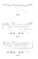
Fig. 1 : Illustration of the façade of the high voltage device with constant current source; -
Fig. 2 : Illustration of A-A section of high voltage device with constant current source of theembodiment 1 seen inFig. 3 ; -
Fig. 3 : Illustration of B-B section of high voltage device with constant current source of theembodiment 1 seen inFig. 2 ; -
Fig. 4 : Illustration of C-C section of high voltage device with constant current source of theembodiment 1 seen inFig. 2 ; -
Fig. 5 : Illustration of the section after step (a) of the high voltage device with constant current source of theembodiment -
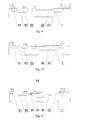
Figs. 6 and 7 : Illustration of the section during step (b) of the high voltage device with constant current source of theembodiment 1; -
Fig. 8 : Illustration of the section after step (c) of the high voltage device with constant current source of theembodiment 1; -
Figs. 9 and 10 : Illustration of the section during step (d) of the high voltage device with constant current source of theembodiment 1; -
Fig. 11 : Illustration of the section after step (e) of the high voltage device with constant current source of theembodiment 1; -
Figs. 12 and 13 : Illustration of the section during step (f) of the high voltage device with constant current source of theembodiment 1; -
Fig. 14 : Illustration of one application circuit of the high voltage device with constant current source; -
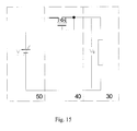
Fig. 15 : Illustration of an alternative application circuit of the high voltage device with constant current source; -
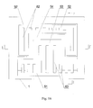
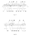
Fig. 16 : Illustration of D-D section of high voltage device with constant current source of theembodiment 2 seen inFig. 17 ; -
Fig. 17 : Illustration of E-E section of high voltage device with constant current source of theembodiment 2 seen inFig. 16 ; -
Fig. 18 : Illustration of F-F section of high voltage device with constant current source of theembodiment 2 seen inFig. 16 ; -
Figs. 19, 20 and 21 : Illustration of the section during step (b) of the high voltage device with constant current source of theembodiment 2; -
Fig. 22 : Illustration of the section after step (c) of the high voltage device with constant current source of theembodiment 2; -
Figs. 23 and 24 : Illustration of the section during step (d) of the high voltage device with constant current source of theembodiment 2; -
Figs. 25 : Illustration of the section after step (e) of the high voltage device with constant current source of theembodiment 2; -
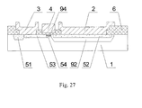
Figs. 26 and27 : Illustration of the section during step (f) of the high voltage device with constant current source of theembodiment 2. - Shown in
Figs. 1-4 , the high voltage device with constant current source of this embodiment 1 consists of P type silicon substrate 1, oxide layer 6 formed on the front face of the silicon substrate 1, drain metal 2, source metal 3, gate metal 4 which are formed on the front face of the oxide layer 6, P+substrate contact region 51, N+drain region 52 and N+source region 53 which are implanted in the silicon substrate 1, N-channel region 54 connecting N+drain region 52 and N+source region 53, N-drain region 92 enveloping N+drain region 52, N-source region 93 enveloping N+source region 53 and P+channel protective region 94 separating N-channel region 54 and the silicon substrate 1; the P+substrate contact region 51 enhances the ohmic contact between the source metal 3 and silicon substrate 1; the P+channel protective region 94 can prevent creepage between the N-channel region 54 and the silicon substrate 1 to further enhance the stability of this device; several drain through holes 82 and source through holes 83 are formed on the oxide layer 6; the drain metal 2 fills the drain through holes 82 and connects N+drain region 52; the source metal 3 fills the source through holes 83, and connects N+source region 53 and P+substrate contact region 51; the source metal 3 and gate metal 4 are electrically connected by connecting metal 34. There is alsoheat sink plane 7 made of titanium, nickel and silver material or an aluminum metal layer on the back of thesilicon substrate 1; thedrain metal 2,source metal 3 andgate metal 4 are made of aluminum, or it may be copper or silicon aluminum alloy. - The high voltage device with constant current source claimed by the invention forms a depletion mode MOSFET which is still kept in a state of getting through when the gate is without voltage to function as an independent high voltage device with constant current source. It is convenient instead of the current peripheral constant voltage and current circuit. Especially, the N-
drain region 92 enhances the electrical isolation between the N+drain region 52 and thesilicon substrate 1 to further the high voltage resistance of the device. In comparison with the device without the said N-drain region 92 and N-source region 93, the high voltage resistance of the high voltage device with constant current source claimed by the invention is raised from 20V to 40V in the range of the constant flow of the current; when it is beyond 40V, due to the temperature characteristic of MOS transistor that the current will decrease under high temperature, it can still be increased to more than 50V although the slope of the voltage curve changes greatly. As a result, this device claimed by the invention can be applied to circuit and absolutely to LED series circuit for the drain avalanche voltage is improved to more than 60V. - It is understood that the
silicon substrate 1 may be N type, but the polar is different. For instance, P+substrate contact region 51 is changed into N+substrate contact region, N+drain 52 into P+drain, N+source 53 into P+source, N-channel region 54 into P-channel region, N-drain 92 into P-drain, N-source 93 into P-source, and P+channelprotective region 94 into N+channel protective region. In such case, it has the same characteristics of the invention. - Shown in
Figs. 4-13 , the steps of manufacturing the high voltage device with constant current source of thisembodiment 1 are as follows: - (a) Formation of oxide layer protection film: Conducting thermal oxidation of P
type silicon substrate 1 in oxidation furnace under 900-1100 °C through wet oxidation to grow the first oxide layer with a thickness of 2000A (controlled within a range of 1000-3000 A), so as to form oxide layer protection film; finally, the section is illustrated inFig. 5 . - (b) Formation of N+drain region, N+source region, N-drain region and N-source region: Executing photoetching on the photoetching machine with the third N+photomask; etching the first oxide layer with corrosive liquid with HF; implanting 1×10¹⁵-1×10¹⁶/cm2 N type impurity arsenic ion in the silicon substrate 1 through ion implanter with an energy of 40-100keV; implanting 1×10¹³∼5×10¹⁵/cm2 N type impurity phosphorus in the silicon substrate 1 through ion implantation with an energy of 40-160keV; shown in
Fig. 6 , or doping phosphorus on the front face of the silicon substrate 1 in high temperature diffusion furnace; then driving the phosphorus and arsenic ion under 1000 - 1200 °C to form, for the diffusion velocity of the phosphorus is faster than that of arsenic ion while the quantity is more than that of arsenic ion, N+drain region 52 and N+source region 53 that are mainly formed by the arsenic ion, N-drain region 92 and N-source region 93 that are mainly formed by the phosphorus, so as to improve the voltage between the drain and source; the N-drain region 92 and N-source region 93 are controlled with a depth of 3-10 microns; meanwhile forming the second oxide layer which is 2000 ∼ 8000 A in thickness; finally, the section is illustrated inFig. 7 . - (c) Formation of P+substrate contact region: Executing photoetching on the photoetching machine with the P+photomask; etching the first and second oxide layers with corrosive liquid with HF; implanting 1×10¹⁴ ∼ 5×10¹⁵/cm2 boron ion or boron difluoride in the
silicon substrate 1 through ion implantation with an energy of 40-160keV; then driving under a high temperature of 1000 ~ 1200 °C to form the said P+substrate contact region 51; meanwhile forming the third oxide layer with a thickness of 1000 ~ 5000 A; finally, the section is illustrated inFig. 8 . - (d) Formation of gate oxide layer: Executing photoetching on the photoetching machine with the gate oxide layer photomask; etching the first, second and third oxide layers with corrosive liquid with HF as shown in
Fig. 9 ; conducting thermal oxidation of the saidsilicon substrate 1 in oxidation furnace under 850 ∼ 1000 °C through dry or wet oxidation to grow the fourth oxide layer with a thickness 1000 A (controlled within a range of 500-2000A), so as to form gate oxide layer; finally, the section is illustrated inFig. 10 . - (e) Formation of N-channel region: Implanting 1×10¹¹ ∼ 1×10¹²/cm2 boron ion in the
silicon substrate 1 between N+drain region 52 and N+source region 53 through ion implantation with an energy of 60-200keV; then implanting 1×10¹¹ ∼ 1×10¹³/cm2 phosphorus in thesilicon substrate 1 between N+drain region 52 and N+source region 53 through ion implantation with an energy of 40-200keV; next, tempering to form the said N-channel region 54 and P+channelprotective region 94; implanting the boron ion is to enhance the concentration of the substrate under the channel to prevent creepage between the drain and source where only surface channel can be gotten through, so the boron ion is usually with more quantity than the phosphorus to ensure the boron ion is deposited beneath the phosphorus after driving; finally, the section is illustrated inFig. 11 . - (f) Formation of metal layer: Executing photoetching on the photoetching machine with contact hole photomask; etching the fourth oxide layer to form the said drain through
hole 82 and source throughhole 83 as shown inFig. 12 ; then depositing metal layer of 10000A thickness (controlled within a range of 5000-30000A) by sputtering or vapour deposition; next executing photoetching on the photoetching machine with metal layer photomask; etching the metal layer to form the saiddrain metal 2,source metal 3,gate metal 4 and connectingmetal 34; finally, the section is illustrated inFig. 13 . - (g) Formation of heat sink plane: Reducing the
silicon substrate 1 by grinding the back thereof from 400 - 650 to 200 - 250 microns to improve the capability of heat dissipation; then depositing an aluminium metal layer or several metal layers containing titanium, nickel and silver by sputtering or vapour deposition on the back of thesilicon substrate 1, so as to form theheat sink plane 7; finally, the section is illustrated inFig. 4 . - An application circuit of the high voltage device with constant current source is shown in
Fig. 14 , which is composed of arectification circuit 10, afilter capacitor 20 and aload 30, as well as a depletion mode MOSFET 40 (i.e. the high voltage device with constant current source claimed by the invention). The AC input end of therectification circuit 10 is connected to AC supply; the DC output end of therectification circuit 10 is in series connection to thefilter capacitor 20; the drain of thedepletion mode MOSFET 40 is connected to one end of the DC output end of therectification circuit 10; the source and gate of thedepletion mode MOSFET 40 are in parallel connection, and connected to one end of theload 30 which is LED assembly or lamps made of several LED in series or parallel connection. In practical application, a series of LED may be firstly in series connection while the total withstand voltage is approximate to and less than the DC voltage after rectification and filtration, then connect the anode of the LED assembly in series connection to the source/gate of the high voltage device with constant current source claimed by the invention of which the drain is connected to the positive voltage after rectification and filtration. Alternatively, the high voltage device with constant current source claimed by the invention is series-wound with the cathode of the LED assembly whose anode is connected to the DC output end of therectification circuit 10, that is to say, theload 30 and thedepletion mode MOSFET 40 exchange places. The saturation current of the high voltage device with constant current source claimed by the invention can be adjusted according to the current of the LED assembly when the gate and source have same potential. Thus, it is able to supply constant current to the LED assembly. Moreover, when the AC voltage is unstable, especially when it exceeds the normal voltage, the additional voltage will be imposed between the drain and source of the high voltage device with constant current source but not to affect the LED assembly, as a result of protecting the LED assembly by stabilized voltage. If AC voltage is less than the normal voltage, it will first reduce the voltage to a value between the drain and source of the high voltage device with constant current source, then the surplus will be shared by the LED assembly equally, which will lead to reduction of the current through LED but neither cause damage to the LED nor cause indispensible power consumption, therefore, it can realize the purpose of energy saving by the LED assembly. For a white light LED working at 3.2V/30mA, if 96 LEDs are connected in series, the total voltage is 307.2V while 220V AC voltage outputs 311 V after rectification and filtration. That is, when the drain of the high voltage device with constant current source whose output current is 30mA is connected to the output end after rectification and filtration, the source and gate are connected to the anode of the LED assembly, the voltage between the drain and source of the high voltage device with constant current source will be up to 3.38V, and the power consumption of the whole circuit will reach about 9.33 W (96×3.2×0.03+3.88×0.03), yet the high voltage device with constant current source only consumes 0.116W (3.88×0.03) which makes up 1.2% of the total power consumption. Because the AC voltage fluctuates ±30V and the DC voltage after rectification and filtration fluctuates±45V, the high voltage device with constant current source can have a function of over voltage protection of the LED assembly under condition of unstable AC supply voltage when the withstand voltage of the high voltage device with constant current source is up to more than 45Y. When applied to LED circuit, this device is able to save the power consumption of the whole circuit. Maybe theload 30 is an electronic circuit or DC motor with high working voltage, even an electric load with high resistance, etc. When applied to LED circuit, the device claimed by the invention has advantages above mentioned. - An alternative application circuit of the high voltage device with constant current source is shown in
Fig. 15 , which is composed of afluctuant DC supply 50, aload 30 made of LED assembly as well as a depletion mode MOSFET 40 (i.e. the high voltage device with constant current source claimed by the invention). The anode input end of thefluctuant DC supply 50 is connected to the drain of the high voltage device with constant current source claimed by the invention; the source and gate of the high voltage device with constant current source are connected to the anode of theload 30 of which the cathode is connected to the cathode of theDC supply 50. Normally, the saturation voltage of N-type depletion mode MOSFET is 1-3V. However, when the output voltage of theDC supply 50 fluctuates between (1.0+V0) and (0.8×Vavalanche voltage+V0), the high voltage device with constant current source claimed by the invention can protect LED load. - As shown in
Figs. 1 ,16 ,17 and 18 , the high voltage device with constant current source of thisembodiment 2 is different from that ofembodiment 1 as follows: The high voltage device with constant current source of thisembodiment 2 is without N-source 93 enveloping the said N+source 53 but with the N-drain 92 enveloping the said N+drain 52, which facilitates simpler structure for the high voltage device with constant current source of thisembodiment 2. - As shown in
Figs. 18-27 , the method of manufacturing the high voltage device with constant current source of thisEmbodiment 2 is different from that ofEmbodiment 1 in step (b). For thisembodiment 2, the step (b) is as follows: Formation of N+drain region, N+source region, N-drain region and N-source region: Executing photoetching on the photoetching machine with the first N+photomask; etching the first oxide layer with corrosive liquid with HF; implanting 1×10¹³ ∼ 5×10¹⁵/cm2 N type impurity phosphorus in thesilicon substrate 1 through ion implantation with an energy of 40-160keV as shown inFig. 19 , or doping phosphorus on the front face of thesilicon substrate 1 in high temperature diffusion furnace; then executing photoetching on the photoetching machine with the second N+photomask; next, etching the first oxide layer with corrosive liquid with HF; implanting 1×10¹⁵-1×10¹⁶/cm2 N type impurity arsenic ion in thesilicon substrate 1 through ion implanter with an energy of 40-100keV as shown inFig. 20 ; driving the phosphorus and arsenic ion under 1000 ∼ 1200 °C to form, for the diffusion velocity of the phosphorus is faster than that of arsenic ion while the quantity is more than that of arsenic ion, N+drain region 52, N+source region 53 and N-drain region 92 so as to improve the withstand voltage between the drain and the source. The N-drain region 92 is controlled with a depth of 3-10 microns; meanwhile forming the second oxide layer which is 2000 - 8000 A in thickness; finally, the section is illustrated inFig. 21 . -
Embodiment 2 is same asEmbodiment 1 for other characteristics. - The invention can be applied to electronic field extensively.
- It is explicitly stated that all features disclosed in the description and/or the claims are intended to be disclosed separately and independently from each other for the purpose of original disclosure as well as for the purpose of restricting the claimed invention independent of the composition of the features in the embodiments and/or the claims. It is explicitly stated that all value ranges or indications of groups of entities disclose every possible intermediate value or intermediate entity for the purpose of original disclosure as well as for the purpose of restricting the claimed invention, in particular as limits of value ranges.
Claims (10)
- A high voltage device with constant current source consists of a P type silicon substrate (1), an oxide layer (6) formed on the front face of the said silicon substrate (1), a drain metal (2), a source metal (3) and a gate metal (4) which are formed on the front face of the said oxide layer (6); wherein it is further composed of a P+substrate contact region (51), an N+drain region (52) and an N+source region (53) which are implanted in the said silicon substrate (1), an N-channel region (54) connected between the said N+drain region (52) and N+source region (53), an N-drain region (92) enveloping the said N+drain region (52); several drain through holes (82) and source through holes (83) are formed on the said oxide layer (6); the said drain metal (2) fills the drain through holes (82) and connects the said N+drain region (52); the said source metal (3) fills the source through holes (83) and connects the said N+source region (53) and P+substrate contact region (51) respectively; the said source metal (3) and gate metal (4) are electrically connected by connecting metal (34).
- The high voltage device with constant current source according to claim 1, wherein further comprises an N-source region (93) enveloping the said N+source region (53).
- The high voltage device with constant current source according to claim 1 or 2, wherein further comprises a P+channel protective region (94) separating the said N-channel region (54) and silicon substrate (1).
- The high voltage device with constant current source according to claim 1 or 2, wherein further comprises on the back a heat sink plane (7) made of one or several metal layers.
- The high voltage device with constant current source according to claim 1 or 2, wherein the said drain metal (2), source metal (3) and gate metal (4) are made of aluminum, copper or silicon aluminum alloy.
- A method of manufacturing the high voltage device with constant current source according to claim 1, wherein it comprises steps as follows:(a) Formation of oxide layer protection film: Conducting thermal oxidation of P type silicon substrate (1) in oxidation furnace through wet oxidation to grow the first oxide layer with a thickness of 1000-3000A, so as to form oxide layer protection film;(b) Formation of N+drain region, N+source region and N-drain region: Executing photoetching on the photoetching machine with the first N+photomask; etching the first oxide layer with corrosive liquid with HF; implanting impurity phosphorus on the front face of the silicon substrate (1) in high temperature diffusion furnace or implanting the impurity phosphorus in the silicon substrate (1) through ion implantation; executing photoetching on the photoetching machine with the second N+photomask; etching the first oxide layer with corrosive liquid with HF; implanting arsenic ion in the said silicon substrate (1) through ion implantation; driving the phosphorus and arsenic ion under high temperature to form, with different diffusion velocity of the phosphorus and arsenic ion, N+drain region (52) and N+source region (53) that are mainly formed by the arsenic ion, N-drain region (92) that is mainly formed by the phosphorus; meanwhile forming a second oxide layer;(c) Formation of P+substrate contact region: Executing photoetching on the photoetching machine with the P+photomask; etching the first and second oxide layers with corrosive liquid with HF; implanting boron ion or P type boron difluoride impurity in the silicon substrate (1) through ion implantation; then driving under high temperature to form the said P+substrate contact region (51); meanwhile forming a third oxide layer;(d) Formation of gate oxide layer: Executing photoetching on the photoetching machine with the gate oxide layer photomask; etching the first, second and third oxide layers with corrosive liquid with HF; conducting thermal oxidation of the said silicon substrate (1) in oxidation furnace through dry or wet oxidation to grow the fourth oxide layer with a thickness of 500-2000A, so as to form a gate oxide layer;(e) Formation of N-channel region: Implanting the phosphorus in the silicon substrate (1) between N+drain region (52) and N+source region (53) through ion implantation; then tempering to form the said N-channel region (54);(f) Formation of metal layer: Executing photoetching on the photoetching machine with contact hole photomask; etching the fourth oxide layer to form the said drain through hole (82) and source through hole (83); then depositing metal layer by sputtering or vapour deposition; next photoetching on the photoetching machine with metal layer photomask; etching the metal layer to form the said drain metal (2), source metal (3), gate metal (4) and connecting metal (34).
- The method of manufacturing the high voltage device with constant current source according to claim 6, wherein the high voltage device with constant current source further comprises a P+channel protective region (94) separating the said N-channel region (54) and silicon substrate (1); in the said step (e), firstly implanting boron ion in the silicon substrate (1) between N+drain region (52) and N+source region (53) through ion implantation; then implanting the phosphorus in the silicon substrate (1) between N+drain region (52) and N+source region (53) through ion implantation; finally tempering to form the said N-channel region (54) and P+channel protective region (94).
- A method of manufacturing the high voltage device with constant current source according to claim 2, wherein it comprises steps as follows:(a) Formation of oxide layer protection film: Conducting thermal oxidation of P type silicon substrate (1) in oxidation furnace through wet oxidation to grow the first oxide layer with a thickness of 1000-3000A, so as to form oxide layer protection film;(b) Formation of N+drain region, N+source region, N-drain region and N-source region: Executing photoetching on the photoetching machine with the third N+photomask; etching the first oxide layer with corrosive liquid with HF; implanting arsenic ion in the silicon substrate (1) through ion implantation; implanting impurity phosphorus on the front face of the silicon substrate (1) in high temperature diffusion furnace or implanting the impurity phosphorus in the silicon substrate (1) through ion implantation; driving the phosphorus and arsenic ion under high temperature to form, with different diffusion velocity of the phosphorus and arsenic ion, N+drain region (52) and N+source region (53) that are mainly formed by the arsenic ion, N-drain region (92) and N-source region (93) that are mainly formed by the phosphorus; meanwhile forming a second oxide layer;(c) Formation of P+substrate contact region: Executing photoetching on the photoetching machine with the P+photomask; etching the first and second oxide layers with corrosive liquid with HF; implanting boron ion or P type boron difluoride impurity in the silicon substrate (1) through ion implantation; then driving under high temperature to form the said P+substrate contact region (51); meanwhile forming a third oxide layer;(d) Formation of gate oxide layer: Executing photoetching on the photoetching machine with the gate oxide layer photomask; etching the first, second and third oxide layers with corrosive liquid with HF; conducting thermal oxidation of the said silicon substrate (1) in oxidation furnace through dry or wet oxidation to grow a fourth oxide layer with a thickness of 500-2000A, so as to form gate oxide layer;(e) Formation of N-channel region: Implanting the phosphorus in the silicon substrate (1) between N+drain region (52) and N+source region (53) through ion implantation; then tempering to form the said N-channel region (54);(f) Formation of metal layer: Executing photoetching on the photoetching machine with contact hole photomask; etching the fourth oxide layer to form the said drain through hole (82) and source through hole (83); then depositing metal layer by sputtering or vapour deposition; next executing photoetching on the photoetching machine with metal layer photomask; etching the metal layer to form the said drain metal (2), source metal (3), gate metal (4) and connecting metal (34).
- The method of manufacturing the high voltage device with constant current source according to claim 8, wherein the high voltage device with constant current source further comprises a P+channel protective region (94) separating the N-channel region (54) and the silicon substrate (1); in the said step (e), firstly implanting boron ion in the silicon substrate (1) between N+drain region (52) and N+source region (53) through ion implantation; then implanting the phosphorus in the silicon substrate (1) between N+drain region (52) and N+source region (53) through ion implantation; finally tempering to form the said N-channel region (54) and P+channel protective region (94).
- The method of manufacturing the high voltage device with constant current source according to one of claims 6-9, wherein on the back there is a heat sink plane (7) made of one or several metal layers; it also includes step (g) following (f): Formation of heat sink plane: Firstly reducing the silicon substrate (1) by grinding the back; then depositing an aluminum metal layer or several metal layers containing titanium, nickel and silver by sputtering or vapor deposition on the back of the silicon substrate (1), so as to form the heat sink plane (7).
Applications Claiming Priority (1)
| Application Number | Priority Date | Filing Date | Title |
|---|---|---|---|
| CN2008100289995A CN101299439B (en) | 2008-06-24 | 2008-06-24 | High pressure resistant constant-current source device and production method |
Publications (1)
| Publication Number | Publication Date |
|---|---|
| EP2139042A1 true EP2139042A1 (en) | 2009-12-30 |
Family
ID=40079192
Family Applications (1)
| Application Number | Title | Priority Date | Filing Date |
|---|---|---|---|
| EP09008062A Withdrawn EP2139042A1 (en) | 2008-06-24 | 2009-06-19 | High voltage device with constant current source and manufacturing method thereof |
Country Status (4)
| Country | Link |
|---|---|
| US (1) | US8169029B2 (en) |
| EP (1) | EP2139042A1 (en) |
| JP (1) | JP2010010680A (en) |
| CN (1) | CN101299439B (en) |
Families Citing this family (11)
| Publication number | Priority date | Publication date | Assignee | Title |
|---|---|---|---|---|
| US8169763B2 (en) * | 2008-06-26 | 2012-05-01 | Bourns, Inc. | Transient blocking unit having an enhancement mode device in the primary current path |
| CN101764101B (en) * | 2008-12-25 | 2012-05-23 | 上海先进半导体制造股份有限公司 | BCD integration process |
| US9818857B2 (en) | 2009-08-04 | 2017-11-14 | Gan Systems Inc. | Fault tolerant design for large area nitride semiconductor devices |
| US9029866B2 (en) | 2009-08-04 | 2015-05-12 | Gan Systems Inc. | Gallium nitride power devices using island topography |
| JP5985393B2 (en) * | 2009-08-04 | 2016-09-06 | ジーエーエヌ システムズ インコーポレイテッド | Island matrix gallium nitride microwave transistor and power switching transistor |
| CN104409431B (en) * | 2014-10-24 | 2017-07-04 | 苏州能讯高能半导体有限公司 | A kind of semiconductor devices |
| US9536945B1 (en) | 2015-07-30 | 2017-01-03 | International Business Machines Corporation | MOSFET with ultra low drain leakage |
| CN106992152B (en) * | 2016-11-30 | 2018-08-28 | 江苏丽隽功率半导体有限公司 | A kind of single-chip making high voltage and constant current IC methods |
| CN109712972B (en) * | 2017-10-26 | 2024-06-04 | 上海维安电子股份有限公司 | Layout structure of overvoltage protection chip |
| JP7342408B2 (en) * | 2019-04-15 | 2023-09-12 | 富士電機株式会社 | semiconductor equipment |
| CN115101522A (en) * | 2022-06-30 | 2022-09-23 | 上海韦尔半导体股份有限公司 | Preparation process of unidirectional high-voltage transient voltage suppression protection device and protection device |
Citations (9)
| Publication number | Priority date | Publication date | Assignee | Title |
|---|---|---|---|---|
| US3440502A (en) * | 1966-07-05 | 1969-04-22 | Westinghouse Electric Corp | Insulated gate field effect transistor structure with reduced current leakage |
| JPS55130171A (en) | 1979-03-29 | 1980-10-08 | Fujitsu Ltd | Mos field effect transistor |
| US4680605A (en) | 1984-03-12 | 1987-07-14 | Xerox Corporation | High voltage depletion mode transistor with serpentine current path |
| US4851360A (en) | 1986-09-29 | 1989-07-25 | Texas Instruments Incorporated | NMOS source/drain doping with both P and As |
| US5893742A (en) | 1995-01-17 | 1999-04-13 | National Semiconductor Corporation | Co-implantation of arsenic and phosphorus in extended drain region for improved performance of high voltage NMOS device |
| US20050205925A1 (en) | 2004-03-22 | 2005-09-22 | Teruo Takizawa | Semiconductor device and method for manufacturing the same |
| US20060170041A1 (en) * | 2005-01-20 | 2006-08-03 | Kabushiki Kaisha Toshiba | MOSFET and optical coupling device having the same |
| US20060275990A1 (en) * | 2005-05-13 | 2006-12-07 | Kazuichiro Itonaga | Semiconductor device and method of producing same |
| EP2065939A2 (en) | 2007-11-28 | 2009-06-03 | Nanker(Guang Zhou)Semiconductor Manufacturing Corp | Constant current source device and method for manufacturing the same |
Family Cites Families (3)
| Publication number | Priority date | Publication date | Assignee | Title |
|---|---|---|---|---|
| USRE28704E (en) * | 1968-03-11 | 1976-02-03 | U.S. Philips Corporation | Semiconductor devices |
| JP3802935B2 (en) * | 1993-07-16 | 2006-08-02 | 三菱電機株式会社 | High voltage semiconductor device |
| US6798022B1 (en) * | 2003-03-11 | 2004-09-28 | Oki Electric Industry Co., Ltd. | Semiconductor device with improved protection from electrostatic discharge |
-
2008
- 2008-06-24 CN CN2008100289995A patent/CN101299439B/en not_active Expired - Fee Related
-
2009
- 2009-06-19 EP EP09008062A patent/EP2139042A1/en not_active Withdrawn
- 2009-06-24 US US12/490,992 patent/US8169029B2/en not_active Expired - Fee Related
- 2009-06-24 JP JP2009149858A patent/JP2010010680A/en active Pending
Patent Citations (9)
| Publication number | Priority date | Publication date | Assignee | Title |
|---|---|---|---|---|
| US3440502A (en) * | 1966-07-05 | 1969-04-22 | Westinghouse Electric Corp | Insulated gate field effect transistor structure with reduced current leakage |
| JPS55130171A (en) | 1979-03-29 | 1980-10-08 | Fujitsu Ltd | Mos field effect transistor |
| US4680605A (en) | 1984-03-12 | 1987-07-14 | Xerox Corporation | High voltage depletion mode transistor with serpentine current path |
| US4851360A (en) | 1986-09-29 | 1989-07-25 | Texas Instruments Incorporated | NMOS source/drain doping with both P and As |
| US5893742A (en) | 1995-01-17 | 1999-04-13 | National Semiconductor Corporation | Co-implantation of arsenic and phosphorus in extended drain region for improved performance of high voltage NMOS device |
| US20050205925A1 (en) | 2004-03-22 | 2005-09-22 | Teruo Takizawa | Semiconductor device and method for manufacturing the same |
| US20060170041A1 (en) * | 2005-01-20 | 2006-08-03 | Kabushiki Kaisha Toshiba | MOSFET and optical coupling device having the same |
| US20060275990A1 (en) * | 2005-05-13 | 2006-12-07 | Kazuichiro Itonaga | Semiconductor device and method of producing same |
| EP2065939A2 (en) | 2007-11-28 | 2009-06-03 | Nanker(Guang Zhou)Semiconductor Manufacturing Corp | Constant current source device and method for manufacturing the same |
Also Published As
| Publication number | Publication date |
|---|---|
| US8169029B2 (en) | 2012-05-01 |
| CN101299439B (en) | 2011-06-22 |
| CN101299439A (en) | 2008-11-05 |
| JP2010010680A (en) | 2010-01-14 |
| US20090315123A1 (en) | 2009-12-24 |
Similar Documents
| Publication | Publication Date | Title |
|---|---|---|
| EP2139042A1 (en) | High voltage device with constant current source and manufacturing method thereof | |
| US6946705B2 (en) | Lateral short-channel DMOS, method of manufacturing the same, and semiconductor device | |
| CN1243334A (en) | Surface voltage-resistant layer of semiconductor device for floating voltage end | |
| EP2860762A1 (en) | High voltage junction field effect transistor | |
| US11264269B1 (en) | Method of manufacturing trench type semiconductor device | |
| TW201344847A (en) | Reference voltage generating device | |
| US20040251493A1 (en) | Lateral short-channel dmos, method for manufacturing same and semiconductor device | |
| US9142401B2 (en) | Semiconductor device and method of manufacturing a semiconductor device with a continuous silicate glass structure | |
| CN100459073C (en) | Lateral double-diffused metal oxide semiconductor element and manufacturing method thereof | |
| US5956582A (en) | Current limiting circuit with continuous metallization | |
| US7632732B2 (en) | Method of manufacturing MOS transistor | |
| EP2172975A2 (en) | Insulated gate bipolar transistor | |
| CN100570891C (en) | High withstand voltage semiconductor device and manufacturing method thereof | |
| CN101452953B (en) | Constant current source device and manufacturing method | |
| US20070246790A1 (en) | Transistor process using a double-epitaxial layer for reduced capacitance | |
| CN112151532B (en) | Semiconductor device for electrostatic protection | |
| US20130099293A1 (en) | Semiconductor structure and method for forming the same | |
| KR101137308B1 (en) | Power mos transistor and manufacturing method for reducing power consumption with surge protection means | |
| CN201222500Y (en) | High pressure-resistant constant flow source device | |
| EP2175488A1 (en) | Semiconductor device and method for manufacturing the same | |
| CN102544065B (en) | Zener diode structure in 60V high-voltage process for bipolar, complementary metal oxide semiconductor (CMOS) and double diffusion metal oxide semiconductor (DMOS) (BCD) devices, and manufacturing method for Zener diode structure | |
| US20040159866A1 (en) | Semiconductor device | |
| CN201134434Y (en) | Constant flow source device | |
| CN204088324U (en) | A kind of isolation structure of high-voltage driving circuit | |
| CN101304048A (en) | New voltage protection device |
Legal Events
| Date | Code | Title | Description |
|---|---|---|---|
| PUAI | Public reference made under article 153(3) epc to a published international application that has entered the european phase |
Free format text: ORIGINAL CODE: 0009012 |
|
| AK | Designated contracting states |
Kind code of ref document: A1 Designated state(s): AT BE BG CH CY CZ DE DK EE ES FI FR GB GR HR HU IE IS IT LI LT LU LV MC MK MT NL NO PL PT RO SE SI SK TR |
|
| 17P | Request for examination filed |
Effective date: 20100608 |
|
| 17Q | First examination report despatched |
Effective date: 20100702 |
|
| STAA | Information on the status of an ep patent application or granted ep patent |
Free format text: STATUS: THE APPLICATION IS DEEMED TO BE WITHDRAWN |
|
| 18D | Application deemed to be withdrawn |
Effective date: 20130724 |