EP2139108A1 - Procédé pour l'amplification de signaux utilisant un système amplificateur de puissance, système amplificateur de puissance, station de base, station mobile et réseau de communication correspondant - Google Patents
Procédé pour l'amplification de signaux utilisant un système amplificateur de puissance, système amplificateur de puissance, station de base, station mobile et réseau de communication correspondant Download PDFInfo
- Publication number
- EP2139108A1 EP2139108A1 EP08158911A EP08158911A EP2139108A1 EP 2139108 A1 EP2139108 A1 EP 2139108A1 EP 08158911 A EP08158911 A EP 08158911A EP 08158911 A EP08158911 A EP 08158911A EP 2139108 A1 EP2139108 A1 EP 2139108A1
- Authority
- EP
- European Patent Office
- Prior art keywords
- power amplifier
- driver
- amplifier system
- transistor
- gate
- Prior art date
- Legal status (The legal status is an assumption and is not a legal conclusion. Google has not performed a legal analysis and makes no representation as to the accuracy of the status listed.)
- Withdrawn
Links
Images


Classifications
-
- H—ELECTRICITY
- H03—ELECTRONIC CIRCUITRY
- H03F—AMPLIFIERS
- H03F3/00—Amplifiers with only discharge tubes or only semiconductor devices as amplifying elements
- H03F3/20—Power amplifiers, e.g. Class B amplifiers, Class C amplifiers
- H03F3/21—Power amplifiers, e.g. Class B amplifiers, Class C amplifiers with semiconductor devices only
- H03F3/217—Class D power amplifiers; Switching amplifiers
-
- H—ELECTRICITY
- H03—ELECTRONIC CIRCUITRY
- H03F—AMPLIFIERS
- H03F3/00—Amplifiers with only discharge tubes or only semiconductor devices as amplifying elements
- H03F3/04—Amplifiers with only discharge tubes or only semiconductor devices as amplifying elements with semiconductor devices only
- H03F3/08—Amplifiers with only discharge tubes or only semiconductor devices as amplifying elements with semiconductor devices only controlled by light
- H03F3/085—Amplifiers with only discharge tubes or only semiconductor devices as amplifying elements with semiconductor devices only controlled by light using opto-couplers between stages
-
- H—ELECTRICITY
- H03—ELECTRONIC CIRCUITRY
- H03F—AMPLIFIERS
- H03F2200/00—Indexing scheme relating to amplifiers
- H03F2200/276—Indexing scheme relating to amplifiers the DC-isolation amplifier, e.g. chopper amplifier, modulation/demodulation amplifier, uses optical isolation means, e.g. optical couplers
-
- H—ELECTRICITY
- H03—ELECTRONIC CIRCUITRY
- H03F—AMPLIFIERS
- H03F2200/00—Indexing scheme relating to amplifiers
- H03F2200/331—Sigma delta modulation being used in an amplifying circuit
-
- H—ELECTRICITY
- H03—ELECTRONIC CIRCUITRY
- H03F—AMPLIFIERS
- H03F2200/00—Indexing scheme relating to amplifiers
- H03F2200/451—Indexing scheme relating to amplifiers the amplifier being a radio frequency amplifier
Definitions
- the invention relates to a power amplifier system according to the preamble of claim 1, a base station according to the preamble of claim 10, a mobile station according to the preamble of claim 11, a communication network according to the preamble of claim 12, and a method for signal amplification using a power amplifier system according to the preamble of claim 13.
- UMTS Universal Mobile Telecommunications System
- 3GPP LTE Third Generation Partnership Project Long Term Evolution
- WIMAX Worldwide Interoperability for Microwave Access
- a new architecture may use so-called switch mode amplifiers, as e.g. class-D/E/F or class-S amplifiers, to improve the power efficiency.
- switch mode amplifiers e.g. class-D/E/F or class-S amplifiers
- the class-S approach inherently leads to higher efficiency of the power amplifier of theoretically 100% and by means of the digital approach reduces analogue imperfections and liability to distortions.
- Switch mode amplifiers as e.g. class S amplifiers, are a preferred architecture, as digital power amplifiers fit the general direction of the architecture for software defined radio (SDR) and thus higher level of digitization of the transceiver, and as the switch mode amplifier architecture is the only architecture offering a 100% theoretical efficiency limit.
- SDR software defined radio
- a Class-AB amplifier architecture for instance can never have an efficiency better than 78% due to fundamental physical limitations. It is above all in the operator's interest to get as close as possible to the theoretical efficiency limit.
- the transistor In said switch mode radio frequency (RF) power amplifiers, the transistor is not amplifying the input signal linearly, but is acting as a switch in the ideal case. As an ideal switch does not dissipate power, a theoretical power efficiency of 100% could be reachable.
- RF radio frequency
- Switch mode power amplifiers can either be realized in a current switched or in a voltage switched mode.
- the basic principle of current switched mode class D power amplifier architecture is disclosed.
- the gate of the switching transistors typically has high input capacitance making it difficult to maintain a good rectangular shape. Smoothing of the rectangular shape by the R-C circuit consisting of the driver's output impedance combined with the input capacitance of the switching transistor may easily lead to a loss of efficiency by 10 to 20%. Simulations have revealed that a 50 Ohm source impedance by the driver is too high, instead a driver with 1 Ohm output impedance is needed.
- the gate drive signal is always referenced to the source of the transistor.
- the source of one transistor is floating, which makes it difficult to drive it.
- the driver circuit would have to provide a very large voltage swing which is difficult to obtain especially with a rectangular signal and a large gate capacitance.
- the object of the invention is thus to provide a power amplifier system offering driving signals of the transistors that have a rectangular shape and allow source potential of the transistors to float.
- a power amplifier system according to the teaching of claim 1
- a base station according to the teaching of claim 10
- a mobile station according to the teaching of claim 11
- a communication network according to the teaching of claim 12
- a method for signal amplification using a power amplifier system according to the teaching of claim 13.
- the main idea of the invention is to no longer use a direct electrical drive of the gate of the transistor, i.e. to no longer use a direct electrical connection from the driver to the gate, but to use light for signal transmission from the driver, so that there is e.g. an optical fiber connected from the driver either to the transistor or to a photo detector that is in turn connected to the transistor.
- Fig. 1 schematically shows a switched mode power amplifier architecture relying on a voltage switched circuit topology according to the state-of-the-art.
- Fig. 2 schematically shows a switched mode power amplifier architecture relying on a current switched circuit topology according to the state-of-the-art.
- Fig. 3 schematically shows a switched mode power amplifier architecture relying on a voltage switched circuit topology using an optical drive and photo detectors according to the invention.
- Fig. 4 schematically shows a switched mode power amplifier architecture relying on a voltage switched circuit topology using an optical drive and phototransistors according to the invention.
- a voltage switched power amplifier system according to the state-of-the-art as shown in fig. 1 comprises a delta-sigma modulator DSM with inputs for reception of a digital or analogue RF input signal RFI and for reception of a clocking signal CS.
- An output of the delta-sigma modulator DSM is connected to an input of a driver DR.
- the delta-sigma modulator DSM is connected to a noise-shaping filter NF.
- a first output of the driver DR is connected to the gate G of a first transistor T1, and a second output of the driver DR is connected to the gate G of a second transistor T2.
- the source S of the first transistor T1 is connected to ground, and the source of the second transistor T2 is connected to the drain of the first transistor T1.
- the drain of the first transistor T1 and the source of the second transistor T2 are connected to an RF output via a reconstruction filter RFILT that comprises an inductor L and a capacitor C in series.
- a reconstruction filter RFILT that comprises an inductor L and a capacitor C in series.
- the drain of the second transistor T2 is connected to the supply of a constant voltage source.
- a method for signal amplification using a voltage switched power amplifier system according to the state-of-the-art as shown in fig. 1 , digital or analogue RF input signals are sent to the delta-sigma modulator DSM. Furthermore, clocking signals with a multiple of the RF carrier frequency are sent to the delta-sigma modulator DSM.
- the digital or analogue RF input signals are converted into digital 1-bit or higher resolution signals using a so-called sample-and-hold output.
- the sampling rate is determined by the received clocking signals.
- the digital 1-bit or multibit signals are provided at the output of the delta-sigma modulator DSM.
- the noise shaping filter NF is used to minimize quantization error by means of shifting quantization noise into frequency ranges that are less or not relevant for signal processing.
- Said digital 1-bit signals are sent to the driver DR that generates first driver signals based on the digital 1-bit signals and second driver signals based on the inverted digital 1-bit signals.
- the first driver signals are sent to the gate of the second transistor T2, and the second driver signals are sent to the gate of the first transistor T1.
- the output signals of the driver DR are thus in antiphase which means if the first transistor T1 is on, the second transistor T2 is off and vice versa.
- the described amplifier architecture with two transistors T1, T2 is just an example, and in alternative architectures, more than two transistors are used, which has however no influence on the invention. Such alternative architectures are e.g. multibit architectures, using two transistors more per each bit more.
- the gate driving signal for transistor T2 is referenced to the source of T2. As the source of T2 is connected to the RF output, this source potential is floating. For transistor T1 the source potential is connected to ground, i.e. it is static.
- the gate-source voltage for "on"-state is typically +1 V and for "off”-state -5 V.
- the gate driving signal for transistor T1 is between -5 V and +1 V.
- the gate driving signal is between -5 V for "off” and +49 V for "on”.
- the capacitor C and the inductor L together build a reconstruction filter RFILT used to generate smooth analogue output signals that are provided at the RF output.
- Fig. 2 shows as a second alternative a switched power amplifier system realized in a current switched mode.
- a current switched power amplifier system according to the state-of-the-art as shown in fig. 2 comprises a delta-sigma modulator DSM with inputs for reception of a digital or analogue RF input signal RFI and for reception of a clocking signal CS.
- An output of the delta-sigma modulator DSM is connected to an input of a driver DR.
- the delta-sigma modulator DSM is connected to a noise-shaping filter NF.
- a first output of the driver DR is connected to the gate of a first transistor T1, and a second output of the driver DR is connected to the gate of a second transistor T2.
- Both the source of the first transistor T1 and the source of the second transistor T2 are connected to ground.
- the drain of the first transistor T1 is connected to a first input of an inductor L and to a first input of a capacitor C
- the drain of the second transistor T2 is connected to a second input of the inductor L and to a second input of the capacitor C.
- the capacitor C and the inductor L build together a reconstruction filter RFILT.
- the supply of a constant current source is connected to a third input of the inductor L.
- the drain of the first transistor T1 is connected to a first input of a balun B
- the drain of the second transistor T2 is connected to a second input of the balun B.
- the balun B transforms a balanced input signal to a single ended signal.
- the analogue RF output signal is provided.
- a method for signal amplification using a current switched power amplifier system according to the state-of-the-art as shown in fig. 2 , digital or analogue RF input signals are sent to the delta-sigma modulator DSM. Furthermore, clocking signals with a multiple of the RF carrier frequency are sent to the delta-sigma modulator DSM.
- the digital or analogue RF input signals are converted into digital 1-bit or higher resolution signals using a so-called sample-and-hold output.
- the sampling rate is determined by the received clocking signals.
- the digital 1-bit or multibit signals are provided at the output of the delta-sigma modulator DSM.
- the noise shaping filter NF is used to minimize quantization error by means of shifting quantization noise into frequency ranges that are less or not relevant for signal processing.
- Said digital 1-bit signals are sent to the driver DR that generates first driver signals based on the digital 1-bit signals and second driver signals based on the inverted digital 1-bit signals.
- the first driver signals are sent to the gate of the first transistor T1, and the second driver signals are sent to the gate of the second transistor T2.
- the output signals of the driver DR are thus in antiphase which means if the first transistor T1 is on, the second transistor T2 is off and vice versa.
- the described amplifier architecture with two transistors T1, T2 is just an example, and in alternative architectures, more than two transistors are used, which has however no influence on the invention. Such alternative architectures are e.g. multibit architectures, using two transistors more per each bit more.
- the first driver signal and the second driver signal respectively are amplified resulting in a first and a second amplifier signal.
- the capacitor C and the inductor L together build a reconstruction filter RFILT used to generate smooth analogue signals out of the first and the second amplifier signals.
- the smoothed first and second analogue signals are sent to the balun B, in which the smoothed first and second analogue signals are added together, thus removing any noise that has been picked up along the way.
- the balun B converts balanced signals to unbalanced signals.
- the unbalanced RF output signals are provided at the output of the balun B.
- the current switched circuit topology needs a balun to transform its balanced output to the typically used single ended lines, which makes the current switched circuit topology more complex and more expensive than the voltage switched circuit topology.
- the power amplifier system comprises at least one optical connection from the driver DR of at least one of said at least two amplifying transistors T1, T2 to at least one processing means with photosensitive material in order to control the gate G of said at least one of said at least two amplifying transistors T1, T2.
- photo detectors comprising said photosensitive material are connected to the gates G.
- This embodiment overcomes the problem with the floating gate G of transistor T2 with the voltage switched circuit topology and ensures symmetry of the two driving paths.
- a second embodiment light is used directly to activate the gates G of the transistors T1 and T2.
- optical fibers are used as optical connections which end above the transistors T1 and T2.
- Specific transistors T1 and T2 with a fiber connector at their housing are needed in this embodiment. With such a configuration, the gate metallization in the transistors T1 and T2 could be removed, whereby the additional problem of large gate capacitances would no longer exist.
- Fig. 3 shows a switched mode power amplifier architecture relying on a voltage switched circuit topology using an optical drive and photo detectors according to the first embodiment of the invention.
- the voltage switched power amplifier system of fig. 3 corresponds to the voltage switched power amplifier system according to the state-of-the-art as shown in fig. 1 with the only difference being the connection between the driver DR and the two transistors T1 and T2.
- a first output of a driver DR is connected by means of an optical fiber OF1 to the input of a first photo detector PD1, and a second output of the driver DR is connected to the input of a second photo detector PD2.
- a first output of the second photo detector PD2 is connected to the gate G of a first transistor T1, and a second output of the second photo detector PD2 is connected to the source S of the first transistor T1.
- a first output of the first photo detector PD1 is connected to the gate G of a second transistor T2, and a second output of the first photo detector PD1 is connected to the source S of the second transistor T2.
- the second output of the second photo detector PD2 is connected to the drain D of the first transistor T1
- the second output of the first photo detector PD1 is connected to the drain D of the second transistor T2.
- the driver DR or the transistors T1 and T2 are fabricated in Gallium Nitride (GaN) technology.
- GaN Gallium Nitride
- the output signals sent from the driver DR are thus optical signals that are sent to the photosensitive material comprised in the photo detectors PD1 and PD2.
- the optical signals create a photo voltage in the photo detectors PD1 and PD2 between the two outputs which is used to drive the gates G.
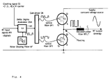
- Fig. 4 shows a switched mode power amplifier architecture relying on a voltage switched circuit topology using an optical drive and phototransistors according to the second embodiment of the invention.
- the voltage switched power amplifier system of fig. 4 corresponds to the voltage switched power amplifier system according to the state-of-the-art as shown in fig. 1 with the only difference being the connection between the driver DR and the two transistors T1 and T2.
- a first output of a driver DR is connected by means of an optical fiber OF2 to a fiber connector of a first phototransistor T1
- a second output of the driver DR is connected to a fiber connector of a second phototransistor T2, i.e. the optical fibers OF1 and OF2 end near to the transistors T1 and T2.
- the transistors T1 and T2 have no gate connectors.
- the driver DR or the transistors T1 and T2 are fabricated in Gallium Nitride (GaN) technology.
- GaN Gallium Nitride
- the output signals sent from the driver DR are thus optical signals that are sent to the photosensitive material comprised in the phototransistors T1 and T2.
- the optical signals create a photo voltage in the phototransistors T1 and T2 which are thus directly activated.
- the optical driver as described can also be used in an analogue way for a current switched power amplifier system as described in fig. 2 , as the optical driver provides equal benefits in overcoming the problem of a large gate capacitance for a current switched power amplifier system.
- a separate driver can be used for each transistor T1 and T2 instead of the common driver DR.
- a separate driver can be used for each transistor T1 and T2 instead of the common driver DR.
- optical fibers OF1 and OF2 instead of optical fibers OF1 and OF2, alternatively optical free space connections between the driver DR and the photosensitive material can be used.
- transistors T1, T2 that comprise gate G, source S and drain D, as e.g. field effect transistors (FET).
- FET field effect transistors
- bipolar transistors T1, T2 that comprise base, emitter and collector can be used for the invention instead.
- Such a power amplifier system according to the invention as described above can be comprised in a transmitter used for transmission in a base station or a mobile station that are part of a communication network.
Landscapes
- Engineering & Computer Science (AREA)
- Power Engineering (AREA)
- Amplifiers (AREA)
Priority Applications (1)
| Application Number | Priority Date | Filing Date | Title |
|---|---|---|---|
| EP08158911A EP2139108A1 (fr) | 2008-06-24 | 2008-06-24 | Procédé pour l'amplification de signaux utilisant un système amplificateur de puissance, système amplificateur de puissance, station de base, station mobile et réseau de communication correspondant |
Applications Claiming Priority (1)
| Application Number | Priority Date | Filing Date | Title |
|---|---|---|---|
| EP08158911A EP2139108A1 (fr) | 2008-06-24 | 2008-06-24 | Procédé pour l'amplification de signaux utilisant un système amplificateur de puissance, système amplificateur de puissance, station de base, station mobile et réseau de communication correspondant |
Publications (1)
| Publication Number | Publication Date |
|---|---|
| EP2139108A1 true EP2139108A1 (fr) | 2009-12-30 |
Family
ID=39929789
Family Applications (1)
| Application Number | Title | Priority Date | Filing Date |
|---|---|---|---|
| EP08158911A Withdrawn EP2139108A1 (fr) | 2008-06-24 | 2008-06-24 | Procédé pour l'amplification de signaux utilisant un système amplificateur de puissance, système amplificateur de puissance, station de base, station mobile et réseau de communication correspondant |
Country Status (1)
| Country | Link |
|---|---|
| EP (1) | EP2139108A1 (fr) |
Citations (2)
| Publication number | Priority date | Publication date | Assignee | Title |
|---|---|---|---|---|
| WO2005017852A2 (fr) * | 2003-08-01 | 2005-02-24 | Bae Systems | Appareil de commande isole equipe de semi-conducteurs de puissance a commande optique |
| US20060140644A1 (en) * | 2004-12-23 | 2006-06-29 | Paolella Arthur C | High performance, high efficiency fiber optic link for analog and RF systems |
-
2008
- 2008-06-24 EP EP08158911A patent/EP2139108A1/fr not_active Withdrawn
Patent Citations (3)
| Publication number | Priority date | Publication date | Assignee | Title |
|---|---|---|---|---|
| WO2005017852A2 (fr) * | 2003-08-01 | 2005-02-24 | Bae Systems | Appareil de commande isole equipe de semi-conducteurs de puissance a commande optique |
| US20050145699A1 (en) * | 2003-08-01 | 2005-07-07 | Oved Zucker | Isolated control apparatus incorporating light controlled power semiconductors |
| US20060140644A1 (en) * | 2004-12-23 | 2006-06-29 | Paolella Arthur C | High performance, high efficiency fiber optic link for analog and RF systems |
Non-Patent Citations (4)
| Title |
|---|
| ASBECK P M ET AL: "Design of High-Efficiency Current-Mode Class-D Amplifiers for Wireless Handsets", IEEE TRANSACTIONS ON MICROWAVE THEORY AND TECHNIQUES, IEEE SERVICE CENTER, PISCATAWAY, NJ, US, vol. 53, no. 1, 1 January 2005 (2005-01-01), pages 144 - 151, XP011125360, ISSN: 0018-9480 * |
| CHOI C-S ET AL: "Phototransistors Based on InP HEMTs and Their Applications to Millimeter-Wave Radio-on-Fiber Systems", IEEE TRANSACTIONS ON MICROWAVE THEORY AND TECHNIQUES, IEEE SERVICE CENTER, PISCATAWAY, NJ, US, vol. 53, no. 1, 1 January 2005 (2005-01-01), pages 256 - 263, XP011125158, ISSN: 0018-9480 * |
| DE BARROS L E M JR ET AL: "Noise performance of HBT as photodetector in analog fiber-optic communication link", MICROWAVE AND OPTOELECTRONICS CONFERENCE, 1997. LINKING TO THE NEXT CE NTURY. PROCEEDINGS., 1997 SBMO/IEEE MTT-S INTERNATIONAL NATAL, BRAZIL 11-14 AUG. 1997, NEW YORK, NY, USA,IEEE, US, vol. 1, 11 August 1997 (1997-08-11), pages 338 - 343, XP010802719, ISBN: 978-0-7803-4165-4 * |
| PAOLELLA A ET AL: "Optically controlled GaAs MMIC switch using a MESFET as an optical detector", 19900508; 19900508 - 19900510, 8 May 1990 (1990-05-08), pages 941 - 944, XP010004601 * |
Similar Documents
| Publication | Publication Date | Title |
|---|---|---|
| KR101235671B1 (ko) | 엔벨로프 제거 및 복원 증폭기를 사용하는 데이터 전송 방법, 엔벨로프 제거 및 복원 증폭기, 전송 디바이스, 수신 디바이스, 및 그것들을 위한 통신 네트워크 | |
| US8385468B2 (en) | Asynchronous delta-sigma modulator and a method for the delta-sigma modulation of an input signal | |
| US6990155B2 (en) | Wireless quadrature modulator transmitter using E/O and O/E connectives | |
| CN103051354B (zh) | 一种片上超低功耗的无线收发装置 | |
| US8908798B2 (en) | Hybrid digital/analog power amplifier | |
| CN101044689A (zh) | 用于无线电路中的功率放大器的信号处理器 | |
| US7683708B2 (en) | Digital amplifier with analogue error correction circuit | |
| US20080129382A1 (en) | High efficiency digital power amplifier | |
| CN114679140B (zh) | 高线性度射频功率放大器 | |
| US9438180B2 (en) | Radio frequency power amplifier and method for increasing power added efficiency and linearity | |
| US8867665B2 (en) | Communication systems and methods supporting multiple modulation techniques | |
| US6411801B1 (en) | Double balanced active mixer | |
| US9281788B2 (en) | All digital zero-voltage switching | |
| EP2139108A1 (fr) | Procédé pour l'amplification de signaux utilisant un système amplificateur de puissance, système amplificateur de puissance, station de base, station mobile et réseau de communication correspondant | |
| KR100978221B1 (ko) | 무선 통신 시스템의 전력 송신 장치 | |
| CN102882476A (zh) | 高频带宽放大电路 | |
| EP2073382A1 (fr) | Procédé pour l'amplification de signaux, système amplificateur d'alimentation commuté, station de base, station mobile et réseau de communication correspondant | |
| EP2408160B1 (fr) | Procédé de transmission de signaux de données à partir d'un dispositif de transmission vers un dispositif de réception au moyen de suivi d'enveloppe pour l'amplification de signal, dispositif de transmission et dispositif de réception correspondant | |
| KR100513970B1 (ko) | 대역폭 향상을 위한 소오스 폴로워 구조의 전치 증폭기 | |
| CN104244138A (zh) | 电流放大器及使用该电流放大器的发射器 | |
| CN117040454A (zh) | 一种毫米波隔离放大器 | |
| KR101952875B1 (ko) | 전력 증폭기 및 이를 포함하는 집적회로 | |
| Zimmermann et al. | Design of an RF-DAC in 65nm CMOS for multistandard, multimode transmitters | |
| Cho et al. | Wideband and multiband long-term evolution transmitter using envelope delta-sigma modulation technique | |
| EP2566071B1 (fr) | Circuit et procédé pour mélanger un signal électrique et optique |
Legal Events
| Date | Code | Title | Description |
|---|---|---|---|
| PUAI | Public reference made under article 153(3) epc to a published international application that has entered the european phase |
Free format text: ORIGINAL CODE: 0009012 |
|
| 17P | Request for examination filed |
Effective date: 20090716 |
|
| AK | Designated contracting states |
Kind code of ref document: A1 Designated state(s): AT BE BG CH CY CZ DE DK EE ES FI FR GB GR HR HU IE IS IT LI LT LU LV MC MT NL NO PL PT RO SE SI SK TR |
|
| AX | Request for extension of the european patent |
Extension state: AL BA MK RS |
|
| RAP1 | Party data changed (applicant data changed or rights of an application transferred) |
Owner name: ALCATEL LUCENT |
|
| AKX | Designation fees paid |
Designated state(s): AT BE BG CH CY CZ DE DK EE ES FI FR GB GR HR HU IE IS IT LI LT LU LV MC MT NL NO PL PT RO SE SI SK TR |
|
| RAP1 | Party data changed (applicant data changed or rights of an application transferred) |
Owner name: ALCATEL LUCENT |
|
| 111Z | Information provided on other rights and legal means of execution |
Free format text: AT BE BG CH CY CZ DE DK EE ES FI FR GB GR HR HU IE IS IT LI LT LU LV MC MT NL NO PL PT RO SE SI SK TR Effective date: 20130410 |
|
| 17Q | First examination report despatched |
Effective date: 20131024 |
|
| STAA | Information on the status of an ep patent application or granted ep patent |
Free format text: STATUS: THE APPLICATION IS DEEMED TO BE WITHDRAWN |
|
| 18D | Application deemed to be withdrawn |
Effective date: 20140105 |
|
| REG | Reference to a national code |
Ref country code: DE Ref legal event code: R079 Free format text: PREVIOUS MAIN CLASS: H03F0003190000 Ipc: H03F0001000000 |
|
| REG | Reference to a national code |
Ref country code: DE Ref legal event code: R079 Free format text: PREVIOUS MAIN CLASS: H03F0003190000 Ipc: H03F0001000000 Effective date: 20140701 |