EP2140282B1 - Dispositif d'annulation cw temporel - Google Patents
Dispositif d'annulation cw temporel Download PDFInfo
- Publication number
- EP2140282B1 EP2140282B1 EP08799737A EP08799737A EP2140282B1 EP 2140282 B1 EP2140282 B1 EP 2140282B1 EP 08799737 A EP08799737 A EP 08799737A EP 08799737 A EP08799737 A EP 08799737A EP 2140282 B1 EP2140282 B1 EP 2140282B1
- Authority
- EP
- European Patent Office
- Prior art keywords
- signal
- time delay
- nuller
- temporal
- output
- Prior art date
- Legal status (The legal status is an assumption and is not a legal conclusion. Google has not performed a legal analysis and makes no representation as to the accuracy of the status listed.)
- Active
Links
Images


Classifications
-
- H—ELECTRICITY
- H04—ELECTRIC COMMUNICATION TECHNIQUE
- H04K—SECRET COMMUNICATION; JAMMING OF COMMUNICATION
- H04K3/00—Jamming of communication; Counter-measures
- H04K3/20—Countermeasures against jamming
- H04K3/22—Countermeasures against jamming including jamming detection and monitoring
- H04K3/224—Countermeasures against jamming including jamming detection and monitoring with countermeasures at transmission and/or reception of the jammed signal, e.g. stopping operation of transmitter or receiver, nulling or enhancing transmitted power in direction of or at frequency of jammer
- H04K3/228—Elimination in the received signal of jamming or of data corrupted by jamming
-
- G—PHYSICS
- G01—MEASURING; TESTING
- G01S—RADIO DIRECTION-FINDING; RADIO NAVIGATION; DETERMINING DISTANCE OR VELOCITY BY USE OF RADIO WAVES; LOCATING OR PRESENCE-DETECTING BY USE OF THE REFLECTION OR RERADIATION OF RADIO WAVES; ANALOGOUS ARRANGEMENTS USING OTHER WAVES
- G01S19/00—Satellite radio beacon positioning systems; Determining position, velocity or attitude using signals transmitted by such systems
- G01S19/01—Satellite radio beacon positioning systems transmitting time-stamped messages, e.g. GPS [Global Positioning System], GLONASS [Global Orbiting Navigation Satellite System] or GALILEO
- G01S19/13—Receivers
- G01S19/21—Interference related issues ; Issues related to cross-correlation, spoofing or other methods of denial of service
-
- H—ELECTRICITY
- H04—ELECTRIC COMMUNICATION TECHNIQUE
- H04K—SECRET COMMUNICATION; JAMMING OF COMMUNICATION
- H04K3/00—Jamming of communication; Counter-measures
- H04K3/80—Jamming or countermeasure characterized by its function
- H04K3/90—Jamming or countermeasure characterized by its function related to allowing or preventing navigation or positioning, e.g. GPS
Definitions
- the present invention relates to global positioning systems and, more particularly, to a device and method for reducing and/or removing narrow band interference/jamming power from a global positioning system receiver's input.
- GPS Global Positioning System
- RF Radio Frequency
- a GPS system receiver determines its terrestrial location by triangulating its position relative to GPS satellites in orbit around the earth, by receiving signals transmitted from the satellites, measuring the travel times of the signals from the satellites to the receiver, and then calculating the distances of the satellites from the receiver based on the travel time.
- very accurate timing is necessary and, therefore, the GPS satellites carry atomic clocks.
- the receiver also needs to know the exact positions of the GPS satellites. In addition, for further accuracy the receiver compensates for atmospheric effects on travel time of the satellite signals to the receiver.
- GPS receiver One basic function of a GPS receiver is to generate replica signals that can be correlated with the received satellite signals.
- Each GPS satellite can have a unique digital code sequence (e.g., a Pseudo Random Code) that is by analogy similar to a musical tune, so that the GPS receiver can distinguish signals from different GPS satellites.
- the GPS receiver knows the "tunes" or code sequences of the different GPS satellites, knows when the "tunes" are to be transmitted, and knows where the GPS satellites should be.
- the GPS receiver Upon receiving a code signal, the GPS receiver identifies the signal, generates a replica of the code signal, and seeks to "hum along" or synchronize the replica signal with the received code, and thereby track the received signal.
- This signal tracking includes two fundamental functions: code-phase tracking to track digital codes of received satellite signals, and carrier-phase tracking to track the carrier signals that are conveying the digital codes.
- code-phase tracking to track digital codes of received satellite signals
- carrier-phase tracking to track the carrier signals that are conveying the digital codes.
- GPS satellites operated by the U.S. military transmit two different signals on two different carrier frequencies.
- the first carrier frequency, L1 has a frequency of 1575.42 MHz and carries two pseudo random digital codes as well as a status message (containing, for example, supplemental information regarding the satellite's orbit, the accuracy of its clock, and so forth).
- the first digital code on L1 is called a C/A (Coarse Acquisition) code.
- the U.S. military makes the C/A code for each U.S. GPS satellite known and available to the public sector.
- the C/A code repeats every 1023 bits, and modulates the L1 carrier frequency at a 1 MHz rate.
- the second carrier frequency, L2 has a frequency of 1227.60 MHz.
- a P(Y) code (“P” for precise, and "(Y)” when the code is encrypted) is also broadcast from each satellite on both the L1 and L2 carrier frequencies.
- the P(Y) codes are intended for exclusive use by the military.
- Each P(Y) code repeats on a 7-day cycle and modulates both the L1 and L2 carrier frequencies at a 10 MHz rate. Transmission of codes on two different carrier frequencies also allows military receivers to estimate atmospheric effects based on the different refractive effects that the atmosphere has on the two different carrier frequencies.
- a problem with conventional GPS receivers is that if they are physically located near or otherwise are in the presence of interference (e.g., narrow band interference/jamming power), successful GPS tracking may not be possible or accuracy may be reduced.
- Prior attempts to address this problem included down converting the L-band GPS signal to a suitable frequency (IF) for digitization and then converting the GPS input signal to the digital domain. Then, while in the digital domain, the narrow band interference is removed using Fourier transformations or other equally complex techniques. For GPS anti-jam applications, once the narrow band interference is removed, the signal is converted back to an IF frequency, and then upconverted to L-band.
- WO-A-2005/050896 discloses a method for suppressing crosstalk from a transmitting antenna by using a phase shifted estimate of the interference signal received in a second antenna.
- a device and method in accordance with present invention enables narrow band interference/jamming power to be easily and efficiently removed from a GPS signal, thereby improving GPS tracking while in the presence of such interference/jamming power.
- the interference/jamming power may be removed by forming a narrow band null in the received GPS signal.
- the null can be formed by splitting an input signal into multiple paths and inserting a delay (preferably a fixed delay) in one path. Further, an adjustable phase shift can be inserted in the delayed path to adjust the frequency at which the null appears.
- the signal processed by the delayed path then can be recombined with a signal processed by a non-delayed path, thereby forming the narrow band null.
- the portion of the signal that passed through the non-delayed path is passed unimpeded to the GPS receiver, while the portion of the signal that passed through the delayed path is rejected by the GPS receiver.
- the fixed delay can be adjusted so that it does not interfere with the GPS receiver's ability to recover the total GPS signal without degradation. This occurs because if the delay is greater than one code chip (e.g., 97 nanoseconds in the case of GPS P(Y) code modulation), the GPS spread spectrum will not correlate with the delayed version. Further, the delayed signal also may be shifted in phase, thereby enabling the null to be tuned for specific frequency ranges, as well as to adjust the power output of the nuller.
- one code chip e.g., 97 nanoseconds in the case of GPS P(Y) code modulation
- the temporal nuller also may include an adjustable phase shifter in the first signal path. The phase shifter enables a frequency at which the null appears to be adjusted.
- a method for removing or minimizing narrow band interference/jamming power from a global positioning system (GPS) receiver's input signal includes forming a narrow band null in at least a portion of the input signal.
- the narrow band null can be formed by splitting a GPS signal into a first signal path and a second signal path, introducing a time delay, which preferably is a fixed time delay, into the first signal path and, recombining the first and second signal paths. Further, an adjustable phase shift may be introduced in the first signal path.
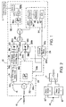
- Fig. 1 is a schematic diagram of an exemplary temporal nuller in accordance with the invention.
- Fig. 2 is a schematic diagram illustrating a plurality of delay elements arranged in a parallel configuration in accordance with the invention.
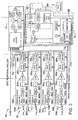
- Fig. 3 is a schematic diagram of an exemplary nuller that includes both a spatial nuller and a temporal nuller in accordance with the invention.
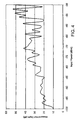
- Fig. 4 is a graph showing measured null depth versus input power for an exemplary temporal nuller in accordance with the invention.
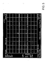
- Fig. 5 is an exemplary spectrum analyzer plot of a null at a particular level of input power for a GPS receiver in accordance with the invention.
- Fig. 6 is a graph showing a magnitude response for two different operational modes of a GPS receiver in accordance with the invention.
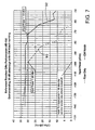
- Fig. 7 is a graph showing reference receiver C/NO performance relative to input power for a GPS receiver in accordance with the invention.
- Fig. 8 is a graph showing the phase locked loop tracking of the GPS signal.
- a block diagram of an exemplary temporal nuller 10 in accordance with the invention is shown, wherein the nuller 10 provides a signal to a GPS receiver 11.
- the GPS temporal nuller 10 can reduce the amplitude of narrow band interference on the GPS receiver 11 by forming nulls in the received GPS signal. Further, the null may be phase shifted so as to alter the frequency or frequencies at which the nulls appear and/or to adjust the power output of the nuller 10. More specifically, by phase shifting the signal, the null location can be adjusted as the frequency in the GPS pass band shifts. As a result, the GPS receiver 11 can operate in areas where narrow band interference and/or jamming power are present.
- an RF (radio frequency) input 12 to the nuller 10 is split into at least two paths.
- a first or primary path 14 (the delayed path) is routed to an input 16a of a delay element 16.
- the delay element 16 may be any circuit, processor, device, etc. that introduces a time delay between a signal presented at the input 16a relative to a signal at the output 16b (e.g., data provided at the input of the delay element is seen at the output of the delay element after a predetermined delay period).
- a delay element is a surface acoustic wave (SAW) device (e.g., a SAW filter).
- SAW surface acoustic wave
- a SAW device is an electromechanical device wherein electrical signals are converted to mechanical acoustic waves in a piezoelectric crystal. This wave is delayed as it propagates across the crystal before being converted back to an electrical signal by further electrodes.
- the delay element preferably is a SAW device, other delay elements may be utilized without departing from the scope of the invention. For example, digital delay lines, optical delays, or the like may be used in place of the SAW device.
- the delay element 16 can be adjustable (i.e., the delay time can be varied) so as to not interfere with the GPS receiver's ability to recover the total GPS signal without degradation or distortion. This occurs because the GPS spread spectrum will not correlate with a delayed version of the signal if the delay is greater than the period for one code chip (97 nanoseconds in the case of GPS P(Y) code modulation).
- the delay can be calculated (e.g., within 1 or more P(Y) code chip delays of the GPS receiver, and preferably 2 P(Y) code chip delays) and the calculated value can be used to select or configure the delay element 16.
- An exemplary delay that can be used in the exemplary temporal nuller 10 is a SAW filter with a delay set for about 225 nanoseconds.
- a single delay element 16 may be utilized for operation in multiple bands (e.g., the L1 band (1575 MHz) and the L2 band (1227 MHz)).
- two different delay elements may be utilized in the first path 14, wherein a first delay element 16' is configured for the L1 frequency band, and a second delay element 16" is configured for the L2 frequency band.
- the two delay elements 16' and 16" may be connected in parallel, and a switch 17 can be coupled to the outputs of the respective delay elements (the switch may be configured or controlled by the controller, which is discussed below).
- the nuller 10 may operate in two different frequency bands (e.g., L1 and L2). As will be appreciated, additional delay elements may be added to further increase the number of nulls or narrow band jammers that can be handled by the nuller.
- the output 16b of the delay element can be provided to an input 18a of phase shifter 18, which can introduce a phase shift into the delayed signal.
- phase shifters change the transmission phase angle of a signal.
- the phase shifter 18 enables the frequencies at which the nulls appear to be adjusted or otherwise varied (e.g., to move the nulls to higher or lower frequency ranges). In other words, the nulls can be tuned to "notch out" the interfering frequency in the GPS band.
- the phase shifter 18 may be a digitally controlled phase shifter, or an analog adjustment of phase (e.g., via pin diodes or via digital switching of pin diodes).
- a phase shift also may be implemented via delay lines, or any other means of introducing a phase shift.
- An output 18b of the phase shifter 18 can be coupled to an input 20a of switch 20.
- Switch 20 includes a select terminal 20b or the like that controls the operation of the switch 20 (the select terminal 20b can be coupled to an output 26a of controller 26, which is discussed in more detail below). For example, if a signal (e.g., a logic 1, TRUE, 3 volts, etc.) is present at the select terminal 20b, the switch will close, thereby coupling the input terminal 20a to the output terminal 20c. If the signal is not present at the select terminal 20b (e.g., a logic 0, FALSE, 0 volts, etc.), then the switch 20 will open and the input terminal 20a will be decoupled from the output terminal 20c. As will be appreciated, other forms of signals may be utilized to operate the switch 20.
- a signal e.g., a logic 1, TRUE, 3 volts, etc.
- the switch 20 will open and the input terminal 20a will be decoupled from the output terminal 20c.
- other forms of signals may be utilized to operate the switch 20.
- the switch 20 may receive commands via a serial communication link or the like (not shown), wherein such signals may be processed by the switch 20 and then acted upon.
- the switch 20 may be an electromechanical switch (e.g., a micro-electro mechanical system switch, micro relay, or the like) or an electrical device (e.g., one or more transistors or the like).
- a secondary path 22 (the non-delayed path) can be routed to a first input 24a of an attenuator 24.
- the attenuator can be used to adjust an amplitude of the primary GPS signal, which can compensate for losses in the primary (i.e., delayed) path 14 (e.g., to compensate for losses created by the delay element 16 and the phase shifter 18) and/or to balance the primary and secondary paths 14 and 22 (e.g., balance the amplitudes of signals in the primary and secondary paths). This enables a deeper, more effective null to be obtained.
- any type of signal attenuator may be used as the attenuator 24.
- Attenuation control can be provided via a second input 24b of the attenuator 24.
- This second input 24b may be coupled to an output 26a of controller 26 and is discussed in more detail below.
- output 26a is shown on the controller 26, it will be appreciated that multiple outputs may exist depending on communication means utilized by the controller. For example, a single output may suffice for parameters communicated via a serial communication link, while multiple outputs may be needed when using discrete outputs and/or inputs.
- the attenuation of the attenuator 24 may be adjusted (e.g., for a 0-10 V signal, 0 V may correspond to minimum attenuation, and 10V may correspond to maximum attenuation).
- An output signal 24c of the attenuator 24 may be provided to an input terminal 28a of switch 28.
- switch 28 also includes a select terminal 28b that controls the operation of the switch 28 (i.e., coupling or decoupling the input terminal 28a from the output terminal 28c).
- the select terminal 28b also may be coupled to the output 26a of controller 26.
- the output 20c, 28c of switches 20, 28, respectively, are combined at summing junction 30 to form a recombined path.
- the recombined path then may be split to go to the nuller output section 32 (which provides the nulled signal to the GPS receiver 11) and a power detection circuit 34.
- the output section 32 can include an attenuator 32a and a filter 32b for conditioning the nulled signal prior to feeding the signal to the GPS receiver 11.
- the power detection circuit 34 measures the output power of the nuller 10, and the measured power in digital form is provided at input 26b of the controller 26 (the controller adjusts nuller parameters to minimize power output as discussed below).
- the power detection circuit 34 implements a log detection function with a 60 dB linear dynamic range, although other types of power detection and/or dynamic ranges may be implemented.
- the power detection circuit 34 can comprise conventional components and can include, for example, a filter 36 (e.g., a low pass filter or the like), an impedance matching circuit 38, a detector circuit 40 for determining the power level, and an analog to digital converter 42 for converting the data to digital form for use by the controller 26.
- An algorithm for controlling the attenuator 24, phase shifter 18 and switches 20 and 28 may be implemented in controller 26 as a field programmable array (FPGA), via code executed by a processor, or the like.
- FPGA field programmable array
- the null depth can be assessed and the optimal settings for the phase shifter 18 and attenuator 24 can be determined and set.
- the controller 26 executes the algorithm stored therein so as to adjust parameters of the nuller 10 that affect power output. By varying an amount of phase shift introduced by the phase shifter 18 and by monitoring the actual power output by the nuller 10, the controller 26 can find an optimum phase shift that produces minimum power output.
- the controller 24 can adjust the attenuation of the attenuator 24 so as to balance the primary and secondary paths 14 and 22 to obtain the same amplitude in both paths.
- controller may configure switches 20 and 28 so as to enable and/or disable operation of the nuller 10. For example, by opening switch 20 and closing switch 28, the nuller 10 operates in reference pass all mode, wherein all signals are pass through the second path 22. In this mode, the nuller 10 is effectively disabled.
- the combined spatial and temporal nuller 50 can include a plurality of multiple antenna paths 52 for receiving the GPS signal, wherein each path can include an antenna 54a-54d coupled to antenna control units 56a-56d.
- Each antenna control unit 56a-56d can include a respective filter 58a-58d, limiter 60a-60d, enable switch 62a-62d, low noise amplifier 64a-64d, antenna interface chip (AIC3) 66a-66d (e.g., an amplifier) and vector controller (VCON) 68a-68d (e.g., a weight network).
- the output of these paths then can be combined and provided to a signal conditioner 70 where they may be band-pass filtered, and then sent to the temporal nuller 10.
- the signal conditioner 70 also may receive a host vehicle RF input (HVRF).
- HVRF host vehicle RF input
- the output of the temporal nuller 10 then can be provided to the GPS receiver 11 as discussed in Fig. 1 , and the receiver can process the GPS signal for navigation purposes.
- the phase and attenuation values of the temporal nuller 10 can be adjusted via the controller 26 (e.g., an algorithm processing unit (APU) or the like that includes or otherwise implements the control algorithm).
- the controller 26 may include memory (both volatile and non-volatile) and a programming port 72 (e.g., a serial port or the like for loading the algorithm). Further, the controller 26 can provide control signals to the time delay device 16, phase shift device 18, the antenna control units 56a-56d, the signal conditioner 70, and the built in test noise source (BIT NS) 74.
- BIT NS built in test noise source
- FIG. 4 an exemplary graph is shown of the nuller performance.
- the data of Fig. 4 was obtained in a closed loop configuration, such that attenuation and phase steps of the CW nuller 10 were under control of the controller 26 (e.g., the nuller algorithm executed by the controller 26 set the phase and attenuation values).
- Fig. 4 illustrates the nulling performance of the temporal nuller 10 against a 1575 MHz CW signal (L1 band).
- the nuller 10 can provide at least 20 dB of performance enhancement against GPS CW interference.
- Fig. 5 is a spectrum analyzer plot of the null at -50 dB CW input.
- Fig. 6 depicts the frequency response measured at the GPS input for two modes; CW nuller mode only 80 (i.e., signals passing through both the first and second paths 14 and 22) and reference pass all mode 82 (i.e., all signals passing only through the second path 22).
- the GPS receiver 8 due to the correlation properties of the spread spectrum signal inside the receiver, will respond to the flat response of reference pass all mode 82 and not the notched response of CW nuller mode 80. As a result, the GPS signal will pass without degradation.
- the nuller performance was limited by a relatively large step size (i.e., 5.6 degrees) for the phase shifter 18.
- Increasing the step size resolution i.e., decreasing the step size would allow for more precise tuning and likely enhanced performance of the nuller 10.
- FIG. 7 illustrates the signal to noise ratio inside a GPS receiver 11 following the CW nuller 10.
- the vertical axis is C/NO (carrier to noise ratio in 1 Hz bandwidth) in dB/Hz, while the horizontal axis is the amplitude of the CW signal at the input of the receiver 11 in dBm.
- the receiver only curve 90 is normal operation without the CW nuller 10, wherein the signal to noise ratio starts degrading for interference powers above -98 dBm.
- the CW notch curve 92 shows the same performance, with the CW nuller 10 putting a null onto the interference. However, the CW notch curve 92 is shifted to the right by about 25 dB, which is the amount of extra interference power that can be tolerated when the CW nuller 10 precedes the GPS receiver 11.
- Fig. 8 shows the phase locked loop (PLL) tracking of the GPS signal. Again, the improvement of tracking versus interference is improved on the order of 25 dB or more.
- PLL phase locked loop
- a simple time delay line and phase shifter can be used to introduce a null that cancels narrow band interference, thereby enhancing a GPS receiver's ability to track its signals.
- the null can be tuned to meet the characteristics of the application.
- the temporal nuller described herein may be implemented using inexpensive and simple components, thereby providing a low cost, reliable solution for countering CW GPS interference.
- Computer program elements of the invention may be embodied in hardware and/or in software (including firmware, resident software, micro-code, etc.).
Landscapes
- Engineering & Computer Science (AREA)
- Radar, Positioning & Navigation (AREA)
- Remote Sensing (AREA)
- Computer Networks & Wireless Communication (AREA)
- Signal Processing (AREA)
- Physics & Mathematics (AREA)
- General Physics & Mathematics (AREA)
- Position Fixing By Use Of Radio Waves (AREA)
- Noise Elimination (AREA)
- Magnetic Resonance Imaging Apparatus (AREA)
- Paper (AREA)
- Variable-Direction Aerials And Aerial Arrays (AREA)
Claims (14)
- Annulateur temporel (10) destiné à éliminer ou minimiser la puissance de brouillage/l'interférence à bande étroite de l'entrée d'un récepteur du système mondial de radiorepérage (GPS), comprenant :un premier chemin de signal (14) comportant un premier noeud d'entrée et un premier noeud de sortie ;au moins un dispositif de retardement (16) placé dans le premier chemin de signal (14), ledit au moins un dispositif de retardement (16) pouvant être mis en oeuvre pour introduire un retard temporel entre un signal au niveau d'une sortie de l'au moins un dispositif de retardement par rapport à un signal au niveau d'une entrée de l'au moins un dispositif de retardement ;un dispositif de déphasage (18) dans le premier chemin de signal (14) pouvant être mis en oeuvre pour introduire un déphasage entre un signal présenté au niveau d'une entrée du dispositif de déphasage et une sortie du dispositif de déphasage ; etun deuxième chemin de signal (22) comportant un deuxième noeud d'entrée et un deuxième noeud de sortie, où le premier noeud d'entrée de signal est connecté électriquement au deuxième noeud d'entrée de signal, et le premier noeud de sortie de signal est connecté électriquement au deuxième noeud de sortie de signal.
- Annulateur temporel de la revendication 1, dans lequel le dispositif de déphasage (18) peut être réglé pour faire varier une grandeur de déphasage introduit par le dispositif de déphasage (18).
- Annulateur temporel selon l'une quelconque des revendications 1 et 2, comprenant en outre un atténuateur (24) placé dans le deuxième chemin de signal (22), ledit atténuateur pouvant être mis en oeuvre pour atténuer un signal dans le deuxième chemin de signal.
- Annulateur temporel selon l'une quelconque des revendications 1-3, comprenant en outre :une unité de commande (26) couplée de manière opérationnelle au dispositif de déphasage (18) ; etun dispositif de détection de puissance (40) couplé de manière opérationnelle aux premier et deuxième noeuds de sortie de signal et à l'unité de commande (26), où ledit dispositif de détection de puissance (40) fournit des données concernant une sortie de puissance au niveau des premier et deuxième noeuds de sortie de signal à l'unité de commande (26), et l'unité de commande peut être mise en oeuvre pour régler le déphasage du dispositif de déphasage (18) de sorte à réaliser une sortie de puissance minimale au niveau des premier et deuxième noeuds de sortie.
- Annulateur temporel selon l'une quelconque des revendications 1-4, dans lequel le dispositif de retardement (16) est un dispositif à ondes acoustiques de surface.
- Annulateur temporel selon l'une quelconque des revendications 1-5, dans lequel le dispositif de retardement (16) peur être réglé pour faire varier une grandeur du retard temporel introduit par le dispositif de retardement.
- Annulateur temporel selon l'une quelconque des revendications 1-6, comprenant en outre un récepteur GPS (11) couplé de manière opérationnelle à une sortie de l'annulateur temporel.
- Annulateur temporel selon l'une quelconque des revendications 1-7, dans lequel l'au moins un dispositif de retardement (16) comporte un premier dispositif de retardement (16') et un deuxième dispositif de retardement (16"), l'annulateur temporel comprenant en outre un commutateur (17) couplé de manière opérationnelle aux premier et deuxième dispositifs de retardement (16', 16"), ledit commutateur pouvant être mis en oeuvre pour relier soit le premier soit le deuxième dispositif de retardement dans le premier chemin de signal.
- Annulateur temporel de la revendication 8, dans lequel le premier dispositif de retardement (16') introduit un retard temporel correspondant à la bande de fréquences L1, et le deuxième dispositif de retardement (16") introduit un retard temporel correspondant à la bande de fréquences L2.
- Procédé destiné à éliminer ou minimiser la puissance de brouillage/l'interférence à bande étroite d'un signal d'entrée d'un récepteur du système mondial de radiorepérage (GPS), comprenant le fait de former un vide de bande étroite dans au moins une partie du signal d'entrée, où la formation du vide de bande étroite comporte le fait :de diviser un signal GPS en un premier chemin de signal et un deuxième chemin de signal ;d'introduire un retard temporel dans le premier chemin de signal pour former le vide ;d'introduire un déphasage dans le premier chemin de signal de sorte à déplacer le vide vers une fréquence dans laquelle apparaît la puissance de brouillage/interférence ; etde recombiner les premier et deuxième chemins de signal.
- Procédé de la revendication 10, comprenant en outre le fait d'atténuer un signal dans le deuxième chemin de signal de sorte à équilibrer une amplitude de signaux dans les premier et deuxième chemins de signal.
- Procédé selon l'une quelconque des revendications 10 et 11, comprenant en outre le fait :de mesurer une sortie de puissance au niveau des premier et deuxième chemins de signal recombinés ; etde régler le déphasage de sorte à réaliser une sortie de puissance minimale au niveau des premier et deuxième chemins de signal recombinés.
- Procédé selon l'une quelconque des revendications 10 à 12, comprenant en outre le fait de fournir les premier et deuxième signaux recombinés à un récepteur GPS.
- Procédé selon l'une quelconque des revendications 10 et 13, comprenant en outre le fait d'introduire plusieurs retards temporels, où chaque retard temporel correspond à une bande de fréquences du signal GPS reçu.
Applications Claiming Priority (2)
| Application Number | Priority Date | Filing Date | Title |
|---|---|---|---|
| US11/693,066 US8159390B2 (en) | 2007-03-29 | 2007-03-29 | Temporal CW nuller |
| PCT/US2008/058176 WO2008121631A2 (fr) | 2007-03-29 | 2008-03-26 | Dispositif d'annulation cw temporel |
Publications (2)
| Publication Number | Publication Date |
|---|---|
| EP2140282A2 EP2140282A2 (fr) | 2010-01-06 |
| EP2140282B1 true EP2140282B1 (fr) | 2011-02-02 |
Family
ID=39739521
Family Applications (1)
| Application Number | Title | Priority Date | Filing Date |
|---|---|---|---|
| EP08799737A Active EP2140282B1 (fr) | 2007-03-29 | 2008-03-26 | Dispositif d'annulation cw temporel |
Country Status (7)
| Country | Link |
|---|---|
| US (1) | US8159390B2 (fr) |
| EP (1) | EP2140282B1 (fr) |
| JP (1) | JP2010532862A (fr) |
| AT (1) | ATE497606T1 (fr) |
| DE (1) | DE602008004831D1 (fr) |
| ES (1) | ES2360392T3 (fr) |
| WO (1) | WO2008121631A2 (fr) |
Families Citing this family (6)
| Publication number | Priority date | Publication date | Assignee | Title |
|---|---|---|---|---|
| TW201024780A (en) * | 2008-12-26 | 2010-07-01 | Altek Corp | Electronic device for decoding navigation data by using phase angle variation and method thereof |
| US9197285B2 (en) * | 2012-12-20 | 2015-11-24 | Deere & Company | Methods and apparatus for ameliorating signal reception |
| WO2014145044A2 (fr) * | 2013-03-15 | 2014-09-18 | Dockon Ag | Égaliseur de ligne adaptatif pour améliorer une transmission de données sur des lignes de transmission ou des lignes électriques qui sont loin d'être parfaites |
| US9391658B2 (en) * | 2014-04-22 | 2016-07-12 | Entropic Communications, Llc | Method and apparatus for cancellation of interference from a spread spectrum phase lock loop |
| US9743293B1 (en) * | 2016-07-25 | 2017-08-22 | Samsung Electronics Co., Ltd. | System and method for local spreading code manipulation for interference mitigation |
| CN108233965B (zh) * | 2017-12-28 | 2020-07-07 | 浙江中智海通信科技有限公司 | 无线数据通信多天线协同接收机架构及其信号接收方法 |
Family Cites Families (21)
| Publication number | Priority date | Publication date | Assignee | Title |
|---|---|---|---|---|
| CA1088632A (fr) * | 1975-06-23 | 1980-10-28 | Nippon Eectric Co., Ltd. | Systeme de reception a diversite d'espace avec combinaison de signaux a phases asservies a un etage de frequence intermediaire |
| US4340872A (en) * | 1980-11-26 | 1982-07-20 | E-Systems, Inc. | Continuously variable piezoelectric crystal delay line |
| FR2628914B1 (fr) * | 1988-03-18 | 1990-06-29 | Alcatel Thomson Faisceaux | Recepteur pour systeme de transmission par voie hertzienne a diversite d'espace, comprenant un combineur de diversite |
| US4952193A (en) * | 1989-03-02 | 1990-08-28 | American Nucleonics Corporation | Interference cancelling system and method |
| US5062148A (en) * | 1989-06-02 | 1991-10-29 | Hewlett-Packard Company | Multi-path fading simulator |
| US5068668A (en) * | 1989-09-06 | 1991-11-26 | Hughes Aircraft Company | Adaptive polarization combining system |
| US5019793A (en) * | 1990-05-21 | 1991-05-28 | Hughes Aircraft Company | Digitally implemented variable phase shifter and amplitude weighting device |
| US5410750A (en) * | 1992-02-24 | 1995-04-25 | Raytheon Company | Interference suppressor for a radio receiver |
| US5304945A (en) * | 1993-04-19 | 1994-04-19 | At&T Bell Laboratories | Low-distortion feed-forward amplifier |
| US5796307A (en) * | 1995-11-16 | 1998-08-18 | Ntt Mobile Communications Network Inc. | Amplifying device having input and output nonlinear phase shifters of opposite phase-frequency characteristics |
| US6094166A (en) * | 1996-07-16 | 2000-07-25 | Metawave Communications Corporation | Conical omni-directional coverage multibeam antenna with parasitic elements |
| US5920278A (en) * | 1997-05-28 | 1999-07-06 | Gregory D. Gibbons | Method and apparatus for identifying, locating, tracking, or communicating with remote objects |
| US5872540A (en) | 1997-06-26 | 1999-02-16 | Electro-Radiation Incorporated | Digital interference suppression system for radio frequency interference cancellation |
| DK0924532T3 (da) * | 1997-11-19 | 2006-07-17 | Imec Vzw | Fremgangsmåde og apparat til modtagelse af GPS/GLONASS-signaler |
| US6115409A (en) * | 1999-06-21 | 2000-09-05 | Envoy Networks, Inc. | Integrated adaptive spatial-temporal system for controlling narrowband and wideband sources of interferences in spread spectrum CDMA receivers |
| US6744316B2 (en) * | 2001-04-19 | 2004-06-01 | Motorola, Inc. | Method and apparatus far reduction of distortion in a transmitter |
| US7657241B2 (en) * | 2002-02-01 | 2010-02-02 | Qualcomm, Incorporated | Distortion reduction calibration |
| US20050069063A1 (en) * | 2003-09-30 | 2005-03-31 | Intel Corporation | Broadband interference cancellation |
| ATE488068T1 (de) * | 2003-11-17 | 2010-11-15 | Quellan Inc | Verfahren und system zur löschung von antennenstörungen |
| US20060009185A1 (en) * | 2004-07-08 | 2006-01-12 | Khosro Shamsaifar | Method and apparatus capable of interference cancellation |
| JP2006145315A (ja) | 2004-11-18 | 2006-06-08 | Seiko Epson Corp | 測位装置 |
-
2007
- 2007-03-29 US US11/693,066 patent/US8159390B2/en active Active
-
2008
- 2008-03-26 DE DE602008004831T patent/DE602008004831D1/de active Active
- 2008-03-26 JP JP2010501174A patent/JP2010532862A/ja active Pending
- 2008-03-26 ES ES08799737T patent/ES2360392T3/es active Active
- 2008-03-26 AT AT08799737T patent/ATE497606T1/de not_active IP Right Cessation
- 2008-03-26 WO PCT/US2008/058176 patent/WO2008121631A2/fr not_active Ceased
- 2008-03-26 EP EP08799737A patent/EP2140282B1/fr active Active
Also Published As
| Publication number | Publication date |
|---|---|
| US20100259437A1 (en) | 2010-10-14 |
| EP2140282A2 (fr) | 2010-01-06 |
| ES2360392T3 (es) | 2011-06-03 |
| WO2008121631A2 (fr) | 2008-10-09 |
| US8159390B2 (en) | 2012-04-17 |
| JP2010532862A (ja) | 2010-10-14 |
| DE602008004831D1 (de) | 2011-03-17 |
| WO2008121631A3 (fr) | 2008-11-20 |
| ATE497606T1 (de) | 2011-02-15 |
Similar Documents
| Publication | Publication Date | Title |
|---|---|---|
| US11671133B2 (en) | Adaptive narrowband and wideband interference rejection for satellite navigation receiver | |
| US9577687B2 (en) | Multiple interferer cancellation for communications systems | |
| KR100563386B1 (ko) | 중계기 | |
| JP3099027B2 (ja) | 交差偏波消去装置および偏波状態補正システム | |
| EP2140282B1 (fr) | Dispositif d'annulation cw temporel | |
| US9612337B2 (en) | Antenna beam forming for tracking a transmitter signal | |
| KR102250942B1 (ko) | 피드-포워드 소거기 | |
| EP2911323A1 (fr) | Procédé et appareil permettant d'étalonner automatiquement des réseaux d'antennes | |
| WO2006026582A2 (fr) | Etalonnage de reseau d'antennes | |
| US9766341B2 (en) | GNSS positioning system employing a reconfigurable antenna subsystem | |
| US9641135B2 (en) | Method for detecting an unbalance and for calibrating a multi-port amplifier of a telecommunications satellite | |
| CA3199676A1 (fr) | Rejet d'interference a bande etroite et a large bande adaptatif pour recepteur de navigation par satellite | |
| JP2009518980A (ja) | 光ファイバ遅延線技術を組み込んだ通信とデータリンクのジャマー | |
| US5363111A (en) | Apparatus and method for spatial nulling of interfering signals | |
| JP2001523906A (ja) | アンテナ設備と、アンテナ設備を操作する方法 | |
| Gaydos et al. | Experimental comparison of digital beamforming interference cancellation algorithms using a software defined radio array | |
| Kundu et al. | Incorporation of anti-jamming techniques in a GPS receiver | |
| WO2006078314A2 (fr) | Recepteur d'echantillonnage selectif | |
| US12334967B2 (en) | Receiver with selected suppression of propagating signals | |
| Rügamer et al. | BaSE-II: A robust and experimental Galileo PRS receiver development platform | |
| US8526550B1 (en) | System and method for wideband interference suppression | |
| US6114983A (en) | Electronic counter measures in radar | |
| US12339392B2 (en) | Devices, systems, and methods for cancellation bandwidth-adjustable nulling of interference | |
| JP2004048204A (ja) | 無線中継装置 | |
| Lee et al. | Design and analysis of switching timing for high power GPS meaconing jammer |
Legal Events
| Date | Code | Title | Description |
|---|---|---|---|
| PUAI | Public reference made under article 153(3) epc to a published international application that has entered the european phase |
Free format text: ORIGINAL CODE: 0009012 |
|
| 17P | Request for examination filed |
Effective date: 20090915 |
|
| AK | Designated contracting states |
Kind code of ref document: A2 Designated state(s): AT BE BG CH CY CZ DE DK EE ES FI FR GB GR HR HU IE IS IT LI LT LU LV MC MT NL NO PL PT RO SE SI SK TR |
|
| GRAP | Despatch of communication of intention to grant a patent |
Free format text: ORIGINAL CODE: EPIDOSNIGR1 |
|
| DAX | Request for extension of the european patent (deleted) | ||
| GRAS | Grant fee paid |
Free format text: ORIGINAL CODE: EPIDOSNIGR3 |
|
| GRAA | (expected) grant |
Free format text: ORIGINAL CODE: 0009210 |
|
| AK | Designated contracting states |
Kind code of ref document: B1 Designated state(s): AT BE BG CH CY CZ DE DK EE ES FI FR GB GR HR HU IE IS IT LI LT LU LV MC MT NL NO PL PT RO SE SI SK TR |
|
| REG | Reference to a national code |
Ref country code: GB Ref legal event code: FG4D |
|
| REG | Reference to a national code |
Ref country code: CH Ref legal event code: EP |
|
| REG | Reference to a national code |
Ref country code: IE Ref legal event code: FG4D |
|
| REF | Corresponds to: |
Ref document number: 602008004831 Country of ref document: DE Date of ref document: 20110317 Kind code of ref document: P |
|
| REG | Reference to a national code |
Ref country code: DE Ref legal event code: R096 Ref document number: 602008004831 Country of ref document: DE Effective date: 20110317 |
|
| REG | Reference to a national code |
Ref country code: SE Ref legal event code: TRGR |
|
| REG | Reference to a national code |
Ref country code: NL Ref legal event code: VDEP Effective date: 20110202 |
|
| REG | Reference to a national code |
Ref country code: ES Ref legal event code: FG2A Ref document number: 2360392 Country of ref document: ES Kind code of ref document: T3 Effective date: 20110603 |
|
| LTIE | Lt: invalidation of european patent or patent extension |
Effective date: 20110202 |
|
| PG25 | Lapsed in a contracting state [announced via postgrant information from national office to epo] |
Ref country code: LT Free format text: LAPSE BECAUSE OF FAILURE TO SUBMIT A TRANSLATION OF THE DESCRIPTION OR TO PAY THE FEE WITHIN THE PRESCRIBED TIME-LIMIT Effective date: 20110202 Ref country code: LV Free format text: LAPSE BECAUSE OF FAILURE TO SUBMIT A TRANSLATION OF THE DESCRIPTION OR TO PAY THE FEE WITHIN THE PRESCRIBED TIME-LIMIT Effective date: 20110202 Ref country code: PT Free format text: LAPSE BECAUSE OF FAILURE TO SUBMIT A TRANSLATION OF THE DESCRIPTION OR TO PAY THE FEE WITHIN THE PRESCRIBED TIME-LIMIT Effective date: 20110602 Ref country code: NO Free format text: LAPSE BECAUSE OF FAILURE TO SUBMIT A TRANSLATION OF THE DESCRIPTION OR TO PAY THE FEE WITHIN THE PRESCRIBED TIME-LIMIT Effective date: 20110502 Ref country code: GR Free format text: LAPSE BECAUSE OF FAILURE TO SUBMIT A TRANSLATION OF THE DESCRIPTION OR TO PAY THE FEE WITHIN THE PRESCRIBED TIME-LIMIT Effective date: 20110503 Ref country code: HR Free format text: LAPSE BECAUSE OF FAILURE TO SUBMIT A TRANSLATION OF THE DESCRIPTION OR TO PAY THE FEE WITHIN THE PRESCRIBED TIME-LIMIT Effective date: 20110202 Ref country code: IS Free format text: LAPSE BECAUSE OF FAILURE TO SUBMIT A TRANSLATION OF THE DESCRIPTION OR TO PAY THE FEE WITHIN THE PRESCRIBED TIME-LIMIT Effective date: 20110602 |
|
| PG25 | Lapsed in a contracting state [announced via postgrant information from national office to epo] |
Ref country code: PL Free format text: LAPSE BECAUSE OF FAILURE TO SUBMIT A TRANSLATION OF THE DESCRIPTION OR TO PAY THE FEE WITHIN THE PRESCRIBED TIME-LIMIT Effective date: 20110202 Ref country code: BG Free format text: LAPSE BECAUSE OF FAILURE TO SUBMIT A TRANSLATION OF THE DESCRIPTION OR TO PAY THE FEE WITHIN THE PRESCRIBED TIME-LIMIT Effective date: 20110502 Ref country code: FI Free format text: LAPSE BECAUSE OF FAILURE TO SUBMIT A TRANSLATION OF THE DESCRIPTION OR TO PAY THE FEE WITHIN THE PRESCRIBED TIME-LIMIT Effective date: 20110202 Ref country code: NL Free format text: LAPSE BECAUSE OF FAILURE TO SUBMIT A TRANSLATION OF THE DESCRIPTION OR TO PAY THE FEE WITHIN THE PRESCRIBED TIME-LIMIT Effective date: 20110202 Ref country code: BE Free format text: LAPSE BECAUSE OF FAILURE TO SUBMIT A TRANSLATION OF THE DESCRIPTION OR TO PAY THE FEE WITHIN THE PRESCRIBED TIME-LIMIT Effective date: 20110202 Ref country code: SI Free format text: LAPSE BECAUSE OF FAILURE TO SUBMIT A TRANSLATION OF THE DESCRIPTION OR TO PAY THE FEE WITHIN THE PRESCRIBED TIME-LIMIT Effective date: 20110202 Ref country code: CY Free format text: LAPSE BECAUSE OF FAILURE TO SUBMIT A TRANSLATION OF THE DESCRIPTION OR TO PAY THE FEE WITHIN THE PRESCRIBED TIME-LIMIT Effective date: 20110202 Ref country code: AT Free format text: LAPSE BECAUSE OF FAILURE TO SUBMIT A TRANSLATION OF THE DESCRIPTION OR TO PAY THE FEE WITHIN THE PRESCRIBED TIME-LIMIT Effective date: 20110202 |
|
| PG25 | Lapsed in a contracting state [announced via postgrant information from national office to epo] |
Ref country code: EE Free format text: LAPSE BECAUSE OF FAILURE TO SUBMIT A TRANSLATION OF THE DESCRIPTION OR TO PAY THE FEE WITHIN THE PRESCRIBED TIME-LIMIT Effective date: 20110202 Ref country code: DK Free format text: LAPSE BECAUSE OF FAILURE TO SUBMIT A TRANSLATION OF THE DESCRIPTION OR TO PAY THE FEE WITHIN THE PRESCRIBED TIME-LIMIT Effective date: 20110202 Ref country code: MC Free format text: LAPSE BECAUSE OF NON-PAYMENT OF DUE FEES Effective date: 20110331 |
|
| PG25 | Lapsed in a contracting state [announced via postgrant information from national office to epo] |
Ref country code: SK Free format text: LAPSE BECAUSE OF FAILURE TO SUBMIT A TRANSLATION OF THE DESCRIPTION OR TO PAY THE FEE WITHIN THE PRESCRIBED TIME-LIMIT Effective date: 20110202 Ref country code: RO Free format text: LAPSE BECAUSE OF FAILURE TO SUBMIT A TRANSLATION OF THE DESCRIPTION OR TO PAY THE FEE WITHIN THE PRESCRIBED TIME-LIMIT Effective date: 20110202 Ref country code: CZ Free format text: LAPSE BECAUSE OF FAILURE TO SUBMIT A TRANSLATION OF THE DESCRIPTION OR TO PAY THE FEE WITHIN THE PRESCRIBED TIME-LIMIT Effective date: 20110202 |
|
| PLBE | No opposition filed within time limit |
Free format text: ORIGINAL CODE: 0009261 |
|
| STAA | Information on the status of an ep patent application or granted ep patent |
Free format text: STATUS: NO OPPOSITION FILED WITHIN TIME LIMIT |
|
| PG25 | Lapsed in a contracting state [announced via postgrant information from national office to epo] |
Ref country code: MT Free format text: LAPSE BECAUSE OF FAILURE TO SUBMIT A TRANSLATION OF THE DESCRIPTION OR TO PAY THE FEE WITHIN THE PRESCRIBED TIME-LIMIT Effective date: 20110202 |
|
| REG | Reference to a national code |
Ref country code: IE Ref legal event code: MM4A |
|
| 26N | No opposition filed |
Effective date: 20111103 |
|
| PG25 | Lapsed in a contracting state [announced via postgrant information from national office to epo] |
Ref country code: IE Free format text: LAPSE BECAUSE OF NON-PAYMENT OF DUE FEES Effective date: 20110326 |
|
| REG | Reference to a national code |
Ref country code: DE Ref legal event code: R097 Ref document number: 602008004831 Country of ref document: DE Effective date: 20111103 |
|
| PG25 | Lapsed in a contracting state [announced via postgrant information from national office to epo] |
Ref country code: IT Free format text: LAPSE BECAUSE OF FAILURE TO SUBMIT A TRANSLATION OF THE DESCRIPTION OR TO PAY THE FEE WITHIN THE PRESCRIBED TIME-LIMIT Effective date: 20110202 |
|
| REG | Reference to a national code |
Ref country code: CH Ref legal event code: PL |
|
| PG25 | Lapsed in a contracting state [announced via postgrant information from national office to epo] |
Ref country code: CH Free format text: LAPSE BECAUSE OF NON-PAYMENT OF DUE FEES Effective date: 20120331 Ref country code: LI Free format text: LAPSE BECAUSE OF NON-PAYMENT OF DUE FEES Effective date: 20120331 |
|
| PG25 | Lapsed in a contracting state [announced via postgrant information from national office to epo] |
Ref country code: LU Free format text: LAPSE BECAUSE OF NON-PAYMENT OF DUE FEES Effective date: 20110326 |
|
| PG25 | Lapsed in a contracting state [announced via postgrant information from national office to epo] |
Ref country code: TR Free format text: LAPSE BECAUSE OF FAILURE TO SUBMIT A TRANSLATION OF THE DESCRIPTION OR TO PAY THE FEE WITHIN THE PRESCRIBED TIME-LIMIT Effective date: 20110202 |
|
| PG25 | Lapsed in a contracting state [announced via postgrant information from national office to epo] |
Ref country code: HU Free format text: LAPSE BECAUSE OF FAILURE TO SUBMIT A TRANSLATION OF THE DESCRIPTION OR TO PAY THE FEE WITHIN THE PRESCRIBED TIME-LIMIT Effective date: 20110202 |
|
| REG | Reference to a national code |
Ref country code: FR Ref legal event code: PLFP Year of fee payment: 9 |
|
| REG | Reference to a national code |
Ref country code: FR Ref legal event code: PLFP Year of fee payment: 10 |
|
| REG | Reference to a national code |
Ref country code: FR Ref legal event code: PLFP Year of fee payment: 11 |
|
| P01 | Opt-out of the competence of the unified patent court (upc) registered |
Effective date: 20230530 |
|
| PGFP | Annual fee paid to national office [announced via postgrant information from national office to epo] |
Ref country code: DE Payment date: 20250218 Year of fee payment: 18 |
|
| PGFP | Annual fee paid to national office [announced via postgrant information from national office to epo] |
Ref country code: SE Payment date: 20250218 Year of fee payment: 18 |
|
| PGFP | Annual fee paid to national office [announced via postgrant information from national office to epo] |
Ref country code: FR Payment date: 20250218 Year of fee payment: 18 |
|
| PGFP | Annual fee paid to national office [announced via postgrant information from national office to epo] |
Ref country code: GB Payment date: 20250221 Year of fee payment: 18 |
|
| PGFP | Annual fee paid to national office [announced via postgrant information from national office to epo] |
Ref country code: ES Payment date: 20250401 Year of fee payment: 18 |