EP2141748A2 - Photovoltaikvorrichtung mit Konzentration und spektraler Aufspaltung des gesammelten Lichtstrahls - Google Patents
Photovoltaikvorrichtung mit Konzentration und spektraler Aufspaltung des gesammelten Lichtstrahls Download PDFInfo
- Publication number
- EP2141748A2 EP2141748A2 EP09163201A EP09163201A EP2141748A2 EP 2141748 A2 EP2141748 A2 EP 2141748A2 EP 09163201 A EP09163201 A EP 09163201A EP 09163201 A EP09163201 A EP 09163201A EP 2141748 A2 EP2141748 A2 EP 2141748A2
- Authority
- EP
- European Patent Office
- Prior art keywords
- cells
- array
- photovoltaic
- photovoltaic device
- mirror
- Prior art date
- Legal status (The legal status is an assumption and is not a legal conclusion. Google has not performed a legal analysis and makes no representation as to the accuracy of the status listed.)
- Granted
Links
- 230000003595 spectral effect Effects 0.000 title claims abstract description 16
- 230000005855 radiation Effects 0.000 claims abstract description 45
- 238000001228 spectrum Methods 0.000 claims abstract description 17
- 210000001747 pupil Anatomy 0.000 claims abstract description 16
- 230000003287 optical effect Effects 0.000 claims abstract description 15
- 229910052751 metal Inorganic materials 0.000 claims description 19
- 239000002184 metal Substances 0.000 claims description 19
- 239000000463 material Substances 0.000 claims description 11
- 239000000758 substrate Substances 0.000 claims description 11
- 238000003491 array Methods 0.000 claims description 10
- 230000008878 coupling Effects 0.000 claims description 6
- 238000010168 coupling process Methods 0.000 claims description 6
- 238000005859 coupling reaction Methods 0.000 claims description 6
- 239000011521 glass Substances 0.000 claims description 5
- 239000007769 metal material Substances 0.000 claims description 5
- 230000002459 sustained effect Effects 0.000 claims description 3
- 239000000919 ceramic Substances 0.000 claims description 2
- 230000000694 effects Effects 0.000 claims description 2
- 239000010445 mica Substances 0.000 claims description 2
- 229910052618 mica group Inorganic materials 0.000 claims description 2
- 230000035945 sensitivity Effects 0.000 abstract description 4
- 238000006243 chemical reaction Methods 0.000 description 10
- 238000005286 illumination Methods 0.000 description 9
- 239000003795 chemical substances by application Substances 0.000 description 8
- 239000010408 film Substances 0.000 description 8
- 239000004065 semiconductor Substances 0.000 description 8
- VYPSYNLAJGMNEJ-UHFFFAOYSA-N Silicium dioxide Chemical compound O=[Si]=O VYPSYNLAJGMNEJ-UHFFFAOYSA-N 0.000 description 7
- 238000000034 method Methods 0.000 description 6
- 229910052782 aluminium Inorganic materials 0.000 description 5
- GWEVSGVZZGPLCZ-UHFFFAOYSA-N Titan oxide Chemical compound O=[Ti]=O GWEVSGVZZGPLCZ-UHFFFAOYSA-N 0.000 description 4
- PXHVJJICTQNCMI-UHFFFAOYSA-N Nickel Chemical compound [Ni] PXHVJJICTQNCMI-UHFFFAOYSA-N 0.000 description 3
- XAGFODPZIPBFFR-UHFFFAOYSA-N aluminium Chemical compound [Al] XAGFODPZIPBFFR-UHFFFAOYSA-N 0.000 description 3
- 230000003667 anti-reflective effect Effects 0.000 description 3
- 239000003989 dielectric material Substances 0.000 description 3
- 239000005350 fused silica glass Substances 0.000 description 3
- 230000017525 heat dissipation Effects 0.000 description 3
- 229910001369 Brass Inorganic materials 0.000 description 2
- RYGMFSIKBFXOCR-UHFFFAOYSA-N Copper Chemical compound [Cu] RYGMFSIKBFXOCR-UHFFFAOYSA-N 0.000 description 2
- RTAQQCXQSZGOHL-UHFFFAOYSA-N Titanium Chemical compound [Ti] RTAQQCXQSZGOHL-UHFFFAOYSA-N 0.000 description 2
- MCMNRKCIXSYSNV-UHFFFAOYSA-N Zirconium dioxide Chemical compound O=[Zr]=O MCMNRKCIXSYSNV-UHFFFAOYSA-N 0.000 description 2
- 229910045601 alloy Inorganic materials 0.000 description 2
- 239000000956 alloy Substances 0.000 description 2
- 239000010951 brass Substances 0.000 description 2
- 229910052681 coesite Inorganic materials 0.000 description 2
- 229910052802 copper Inorganic materials 0.000 description 2
- 239000010949 copper Substances 0.000 description 2
- 229910052906 cristobalite Inorganic materials 0.000 description 2
- 229910001234 light alloy Inorganic materials 0.000 description 2
- 229910052759 nickel Inorganic materials 0.000 description 2
- 230000008520 organization Effects 0.000 description 2
- 230000001681 protective effect Effects 0.000 description 2
- 230000001105 regulatory effect Effects 0.000 description 2
- 238000007789 sealing Methods 0.000 description 2
- 239000000377 silicon dioxide Substances 0.000 description 2
- 229920002379 silicone rubber Polymers 0.000 description 2
- 229910052709 silver Inorganic materials 0.000 description 2
- 229910052682 stishovite Inorganic materials 0.000 description 2
- 239000010936 titanium Substances 0.000 description 2
- 229910052719 titanium Inorganic materials 0.000 description 2
- 229910052905 tridymite Inorganic materials 0.000 description 2
- 238000009966 trimming Methods 0.000 description 2
- 229910000838 Al alloy Inorganic materials 0.000 description 1
- 229910000906 Bronze Inorganic materials 0.000 description 1
- 229910001218 Gallium arsenide Inorganic materials 0.000 description 1
- 229910000990 Ni alloy Inorganic materials 0.000 description 1
- 230000033228 biological regulation Effects 0.000 description 1
- 230000005540 biological transmission Effects 0.000 description 1
- 230000015572 biosynthetic process Effects 0.000 description 1
- 239000010974 bronze Substances 0.000 description 1
- 238000005266 casting Methods 0.000 description 1
- 230000015556 catabolic process Effects 0.000 description 1
- 239000011195 cermet Substances 0.000 description 1
- 239000002131 composite material Substances 0.000 description 1
- 239000012141 concentrate Substances 0.000 description 1
- 230000001143 conditioned effect Effects 0.000 description 1
- KUNSUQLRTQLHQQ-UHFFFAOYSA-N copper tin Chemical compound [Cu].[Sn] KUNSUQLRTQLHQQ-UHFFFAOYSA-N 0.000 description 1
- 238000006731 degradation reaction Methods 0.000 description 1
- 238000000151 deposition Methods 0.000 description 1
- 239000000428 dust Substances 0.000 description 1
- 229920001971 elastomer Polymers 0.000 description 1
- 239000000806 elastomer Substances 0.000 description 1
- 238000010292 electrical insulation Methods 0.000 description 1
- 230000002708 enhancing effect Effects 0.000 description 1
- 229910052737 gold Inorganic materials 0.000 description 1
- 229910000856 hastalloy Inorganic materials 0.000 description 1
- 238000009413 insulation Methods 0.000 description 1
- 229910001635 magnesium fluoride Inorganic materials 0.000 description 1
- 229910001092 metal group alloy Inorganic materials 0.000 description 1
- 238000000059 patterning Methods 0.000 description 1
- 229920001084 poly(chloroprene) Polymers 0.000 description 1
- -1 rain Substances 0.000 description 1
- 230000009467 reduction Effects 0.000 description 1
- 239000004071 soot Substances 0.000 description 1
- PBCFLUZVCVVTBY-UHFFFAOYSA-N tantalum pentoxide Inorganic materials O=[Ta](=O)O[Ta](=O)=O PBCFLUZVCVVTBY-UHFFFAOYSA-N 0.000 description 1
- 230000008719 thickening Effects 0.000 description 1
- 239000010409 thin film Substances 0.000 description 1
- 239000012780 transparent material Substances 0.000 description 1
- 230000005641 tunneling Effects 0.000 description 1
Images


Classifications
-
- H—ELECTRICITY
- H10—SEMICONDUCTOR DEVICES; ELECTRIC SOLID-STATE DEVICES NOT OTHERWISE PROVIDED FOR
- H10F—INORGANIC SEMICONDUCTOR DEVICES SENSITIVE TO INFRARED RADIATION, LIGHT, ELECTROMAGNETIC RADIATION OF SHORTER WAVELENGTH OR CORPUSCULAR RADIATION
- H10F77/00—Constructional details of devices covered by this subclass
- H10F77/40—Optical elements or arrangements
-
- H—ELECTRICITY
- H10—SEMICONDUCTOR DEVICES; ELECTRIC SOLID-STATE DEVICES NOT OTHERWISE PROVIDED FOR
- H10F—INORGANIC SEMICONDUCTOR DEVICES SENSITIVE TO INFRARED RADIATION, LIGHT, ELECTROMAGNETIC RADIATION OF SHORTER WAVELENGTH OR CORPUSCULAR RADIATION
- H10F77/00—Constructional details of devices covered by this subclass
- H10F77/40—Optical elements or arrangements
- H10F77/42—Optical elements or arrangements directly associated or integrated with photovoltaic cells, e.g. light-reflecting means or light-concentrating means
- H10F77/488—Reflecting light-concentrating means, e.g. parabolic mirrors or concentrators using total internal reflection
-
- Y—GENERAL TAGGING OF NEW TECHNOLOGICAL DEVELOPMENTS; GENERAL TAGGING OF CROSS-SECTIONAL TECHNOLOGIES SPANNING OVER SEVERAL SECTIONS OF THE IPC; TECHNICAL SUBJECTS COVERED BY FORMER USPC CROSS-REFERENCE ART COLLECTIONS [XRACs] AND DIGESTS
- Y02—TECHNOLOGIES OR APPLICATIONS FOR MITIGATION OR ADAPTATION AGAINST CLIMATE CHANGE
- Y02E—REDUCTION OF GREENHOUSE GAS [GHG] EMISSIONS, RELATED TO ENERGY GENERATION, TRANSMISSION OR DISTRIBUTION
- Y02E10/00—Energy generation through renewable energy sources
- Y02E10/50—Photovoltaic [PV] energy
- Y02E10/52—PV systems with concentrators
Definitions
- This disclosure relates in general to photovoltaic power plants with concentration of radiation and more particularly to a photovoltaic device with concentration and spectral fractioning of the collected radiation.
- Photovoltaic power plants with light concentration allow to reduce usage of expensive semiconductor, typically in form of "discrete" cells of enhanced conversion efficiency that may be arranged on an appropriate substrate in closely packed arrays composed of up to several tens of cells, each with an active area that may be from about 0.5 to about 4 cm 2 , or even larger.
- the cells may be of various types.
- a stack structure of high efficiency double or triple junction cells may comprise a topmost semiconductor layer of GaInP 2 over an intermediate semiconductor layer of GaAs, grown over a substrate of intermediate monocrystalline Ge.
- the junctions between the top and the intermediate semiconductor layer and between the latter layer and the substrate layer constitute two tunneling junctions.
- a rear metal layer and a metal contact realized on the top semiconductor layer, constitute the electric terminals of the cells.
- the surface area of the top semiconductor layer of GaInP 2 not covered by the metal contact represents the active area of the cell and may be provided with an reflective transparent film.
- the overall conversion efficiency of the system may be significantly increased by splitting the spectrum of the collected radiation and to direct beams of different spectrum towards the active surfaces of respectively dedicated cells in order to exploit the largest sensitivity to radiation with wavelength comprised in the specific spectrum of maximum efficiency of the different cells.
- parabolic mirrors for collecting and concentrating radiation in a beam.
- the beam is suitable for illuminating the active areas of the cells that, instead of having a continuous reflective parabolic surface, the mirror surface may be composed of a plurality of planar polyhedral mirrors that approximate a parabolic surface and wherein each planar polyhedral mirror tile that form the parabolic surface has superposed semi-reflective dichroic filter layers over a fully-reflective substrate layer.
- the three or more reflective surfaces of different focal distances concentrate the solar spectrum in three distinct focuses, the relative beams of which are directed onto three cells or arrays of cells with characteristics optimized for the specific region of the spectrum.
- An objective of the Applicant is to provide a photovoltaic device with concentration of the collected radiation and spectral splitting that does not require externally positioned complex light collecting and concentrating and spectrally conditioned focusing optical structures of large dimensions and in which, except for the collection and concentration mirror of the radiation, that necessarily shall have a relatively large size, all other optical elements and every conversion semiconductor devices sensitive to direct exposure to atmospheric agents are enclosed in a hermetically sealed box-like body, protected from dirt and effects of direct exposure to atmospheric agents.
- a photovoltaic device comprising a plurality of photovoltaic cells of different spectral sensitivity, disposed on respective areas of inner surfaces of a hermetically sealed box-like body provided with a transparent pupil with anti-reflection treatment of its surface.
- a concentrated beam of collected radiation enters the device and a plurality of dichroic filters arranged in cascade on the optical axis of the transparent input pupil split the concentrated beam in distinct beams of different spectrum.
- each having multiple reflecting surfaces intercept respective beams of spectral subdivision, and the multiple reflecting surfaces redirect the radiation in form of a plurality of reflected beams each directed to illuminate the active area of a photovoltaic cells of a respective array.
- the collecting parabolic mirror for concentrating solar radiation on the surface of a counter-mirror (not depicted in the figure, typically having the same focal point of the collection mirror, but much closer thereto for reducing its size and thus shadowing) and the related supporting structure are schematically illustrated by the traces 1 and 2 of a portion of the whole collection structure that may have a size in the order of one or more meters.
- the box-like body 3 defines an inner space hermetically isolated from atmospheric agents such as rain, dust, soot and the like.
- the box-like body 3 may be of any material resistant to corrosive actions of atmospheric agents and at least partially of a metallic material of good thermal conductivity, and has at least an opening sealed by a pupil P of a transparent material.
- Aluminum and alloys thereof, copper, brass, titanium are exemplary metallic material suitable for building the hermetically sealed box-like body 3 or at least some parts thereof.
- the pupil P may be made of fused silica and preferably has on both faces a film of anti-reflective material that may include thin films of materials of different refraction index, such as for example MgO, ITO, Ta 2 O 5 , ZrO 2 , TiO 2 , SiO 2 , MgF 2 or other material with suitable optical properties, resistant to atmospheric agents and to the functioning conditions of the photovoltaic device.
- a film of anti-reflective material may include thin films of materials of different refraction index, such as for example MgO, ITO, Ta 2 O 5 , ZrO 2 , TiO 2 , SiO 2 , MgF 2 or other material with suitable optical properties, resistant to atmospheric agents and to the functioning conditions of the photovoltaic device.
- the entrance pupil P of the concentrated beam F1 of collected radiation slightly protrudes from the parabolic surface of the primary mirror 1 through an opening thereof, toward which, in collimation with the optical axis of the entrance pupil, the concentrated primary beam F1 is directed from the focal counter-mirror of the collection parabolic mirror.
- the pupil P may flush or even be slightly recessed from the aperture of the parabolic mirror and reached by the concentrated beam through the aperture.
- the whole box-like body 3 or large part thereof may be made of high conductivity metal with common carpentry and assembly techniques of component pieces ensuring an air-tight sealing from external atmospheric agents, or may be composed of cast or molded parts of a metal alloy having appropriate characteristics of small thermal elongation, lightness and mechanical strength.
- Aluminum, aluminum alloys, light alloys, copper, bronze, brass, titanium, nickel and nickel alloys such as the class of Hastelloy alloys, are exemplary materials that can be used for making the box-like body 3.
- the box-like body 3 may be of cast aluminum light alloy closed hermetically by a flat cover with an appropriate gasket (for example of silicon rubber or other elastomer resistant to atmospheric agents), not depicted in the figure, the shapes of which may be easily determined by the skilled reader.
- an appropriate gasket for example of silicon rubber or other elastomer resistant to atmospheric agents
- a thickening 4 of the metal facilitates the formation of a thicker wall 4 provided with an adequate external finning 5 for favoring dissipation of heat generated by unconverted radiation by the photovoltaic cells of the array distinct arrays C1, C2 and C3 of photovoltaic cells disposed on the inner surface of the thickened wall 4.
- the box-like base of the body 3 may be provided with appropriate internal brackets for mounting and fixing at positions of maximum collimation dichroic filters 6 and 7 in cascade for splitting the primary beam F1 in three distinct beams F2, F3 and F4 spectral splitting by the respective mirrors 8, 9 and 10.
- the surfaces of the inner fixing areas of boards 11, 12 and 13, upon which discrete photovoltaic cells are organized will be adequately planar and smooth for enhancing thermal coupling with the boards.
- the two dichroic filters in cascade 6 and 7 installed along the optical entrance axis, of the primary beam of concentrated radiation F1 through the pupil P, split the primary beam in distinct beams F2, F3 and F4, each having a different spectrum from the others.
- a different number of spectral splitting filters of the collected radiation may be deployed.
- the first dichroic filter 4 may be a layer of fused silica of a thickness of one or more millimeters, having on the surface exposed to the incident radiation a stack of films of different optical characteristics and thickness adapted to reflect the "blue" region of the solar spectrum and let pass radiation of other regions of the solar spectrum.
- the second dichroic filter may also be a layer of fused silica having on the surface exposed to the incident radiation a different stack of films of different optical characteristics and thickness adapted to reflect the "green” region of the solar spectrum and to let pass radiation of the "red” region.
- Each beam of spectral subdivision of the concentrated primary beam F1 is intercepted by a respective mirror 6, 7 or 8, that generally has a plurality of reflecting surfaces, for example a plurality of facets of appropriate incidence angles in respect to the collimated, concentrated and spectrally filtered beam of collected radiation, such to subdivide the reflected radiation into a plurality of beams, typically with divergent axis, each directed to illuminate the active area of a single or of a plurality of adjacent photovoltaic cells of a respective array of cells having their peak sensitivity centered or at least comprised in the spectrum of wavelength of the spectral subdivision beam of the collected radiation.
- a transparent anti-reflective layer is common optical matching techniques.
- the three distinct arrays C1, C2 and C3, of photovoltaic cells are disposed over respective areas of inner surfaces of the box-like body 3, advantageously spatially distributed not to be contiguous or too close to each other, in order to space apart the zones subjected to warm up because of the heat generated by impinging radiation unconverted by the photovoltaic cells of the receiving array.
- a good thermal coupling through the supporting board of the cells of each array with an external heat sink 3 ensures dissipation to atmosphere of heat generated inside the hermetically sealed box-like body by the unconverted radiation.
- the outer surface of the hermetically sealed box-like body 3 may be shaped as a (or alternatively thermally coupled to) dissipating body, typically finned or with a shape adapted to favor heat dissipation in the atmosphere, at least in direct correspondence with the areas of application on the inner surface of the wall of an array of photovoltaic cells.
- dissipation fins 5 protrude out of the outer surface of a thickened zone 4 of the perimetrical metallic wall of the body 3.
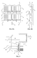
- the organization of discrete photovoltaic cells to realize an array of cells with optimized characteristics for a particular region of the spectrum of the solar radiation according to a certain series-parallel scheme may assume a layout as that illustrated schematically in FIG. 2a and in the layout view of FIG. 2B .
- the single discrete photovoltaic cells 11 may have a rectangular active area (section), partially hidden (masked) by the profile of the structure shaped as a comb-like collector of a metal layer 14 of upper electrical contact of the structure with a plurality of junctions of the photovoltaic cell.
- the metal structure of the upper contact 14 will have a layout adapted to minimize blinding that is the reduction of active area of the cell illuminated by the radiation.
- each photovoltaic cell may be commonly established by proper patterning of the metal layer 15 on the surface of a printed circuit board (PCB) upon which also terminal collector parts 15, connectable through bond wires 16 to electrical pads of the receiving assembly of photoelectric conversion of the collected radiation (not depicted in figure), may be defined.
- PCB printed circuit board
- connection according to the design series-parallel scheme of the array of cells may be commonly realized with bond wires 17 welded upon pads of the upper contact metal layer 14 and upon pads, properly defined, of the superficial metal layer 15 of the board upon which it lays, thus establishing also the electric connection of each photovoltaic cell 11, according to common assembly techniques of electronic devices on PCB.
- FIG. 2B is an elevation view of the board that carries the cells, the substrate layer of dielectric material 18 of which must withstand to the relatively high temperatures due to conversion into heat of the part of radiation that is not converted by the photovoltaic cells.
- a thin ceramic layer, or a glass layer or a cermet with adequate dielectric characteristics is suitable for this application even if other materials with similar characteristics may be used.
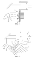
- FIG. 3 depicts an embodiment of the device of this invention that uses a stepped mirror with planar reflecting surfaces.
- FIG. 3 illustrates the stepped shape of the mirror 8sp that intercepts the beam F2, spectrally split from the primary beam F1.
- the multiple planar reflecting surfaces 8' and 8" illuminate the active areas of the photovoltaic cells 11, juxtaposed along respective rows of the array C1.
- the cells array may have a theoretically unlimited number of rows and of columns and correspondingly the stepped mirror will have a number of distinct reflecting surfaces equal to the number of rows of the cell array.
- the relatively thick body 18 of dielectric material of low thermal conductivity may have holes, drilled underneath the fixing pads of the cells, filled with a heat conducting metallic material, that may be planarized on the coupling face of the board.
- the plurality of metal filled holes establish effective thermal bridges 19 of heat conduction from the bottom of the photovoltaic cells 11 towards the coupling wall and the necessary electric insulation of the bottom contacts of the cells is in this case ensured by a thin dielectric layer 20 that being not required to possess any significant mechanical strength and may be made thin enough not to hinder heat transmission from the bottom of the cells to the externally finned metal wall of the box-like body 3.
- Thin layers of mica or of any other suitable dielectric may be used according to common assembling techniques of electronic components.
- FIG. 4 illustrates a partial schematic sectional view of another embodiment wherein the cells 11 of a row may have active areas of identical or different size from the active area of the cells disposed along another row of the array.
- an illumination mirror of the active areas of the array 8sp still having a stepwise geometry with the different reflecting surfaces 8' and 8" having different convex profiles differentiating the "opening" of the reflected beams in order to illuminate the active areas of the cells with substantially the same density of luminous energy even if of different size and/or disposed at different distance from the respective convex reflecting surface.
- the entering beam F1 concentrated by the primary mirror and by the counter-mirror of fixed and non easily modifiable size as also is the active area of the discrete cells deployed it is useful to be able to vary the illumination energy density of the cells of the distinct arrays for the spectral subdivision regions of the collected radiation, in an installed and functioning conversion apparatus by modifying either the curvature of the reflecting surfaces of the stepped mirror or the inclination of the planar array of cells such to attain a satisfactory density of illumination of the active areas of the cells.
- the alternative embodiment of a device contemplates the possibility that the arrays of photovoltaic cells be oriented at a certain angle of inclination from the optical axis of the entering beam F1 as shown in FIGS. 5 , 6 and 7 , instead of being in parallel or orthogonally to it.
- the thicknesses of the anti-reflective multi-layer films present on the surface of the active area of the cells should be adapted to the incidence angle of the light beam.
- the array C1 of photovoltaic cells 11 may be inclined at a certain angle from the reference optical axis of the entering concentrated beam F1.
- a stepped mirror 8sp with planar reflecting surfaces may be used as shown or, in case of cells of different active area, a stepped mirror with convex reflecting surfaces may be used, similarly to what already illustrated in relation to the embodiment of FIG. 4 .
- the possibility of adjusting the angle of inclination of the array within a certain range allows to increase or reduce the incident energy density on the active area of the cells of the array, adapting it to the working characteristics of the cells.
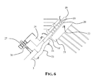
- FIG. 6 An embodiment with enhanced capacity of regulating the energy density for optimal illumination of the active area of the photovoltaic cells, depending on appropriate functioning parameters of the cells, is illustrated in FIG. 6 .
- the array of photovoltaic cells commonly assembled on a printed circuit board may be associated to a finned heat dissipation body, securing electrical insulation and a good thermal coupling between the array of cells organized on a printed circuit board and the dissipating body 21, for example by interposing a thin dielectric film 20, to form an essentially rigid composite panel.
- the assembly is capable of oscillating around a bearing pivot 22 passing through a hole that crosses from side to side the dissipating body 21 and the ends of which are rotatably sustained in appropriate supports (not shown in the cited figure) integral with the outer side of the box-like body 3, that project themselves in proximity of the edge of an aperture through the wall of the box-like body 3 of size sufficient to contain the substantially planar rigid assembly of the array and of the dissipating body.
- Hermeticity of the inner space of the box-like body 3 is ensured by a flexible sealing gasket 23 applied around the whole perimeter of a projecting portion in form of a perimetral flange 18' of the substrate of the printed circuit board that carries the cells, fixed for example with a plurality of bolts 24 that may be tightened onto an eventual counterflange.
- At least a double "L" or step bracket 25 is fixed to an end of the printed circuit board 18 and its position in respect to a threaded pivot 26 integral to the inner wall of the box-like body may be modified by shifting an adjustment nut 27 mechanically connected to the bracket 25, along the threaded pivot 26, according to common automatic positioning techniques along an axis (i.e. axis of the threaded pivot 26).
- the final disposition of the array of cells and in particular the slope angle may be trimmed for optimizing the energy density of illumination of the active areas of the cells of the array, once the mirror that splits the radiation in beams directed toward the active areas of the cells of the array has been set in place.
- Mounting the array with an adjustment fulcrum 22 and the possibility of varying the slope angle with common actuating means, typically electromagnetic means, offer the possibility of implementing a closed loop control systems capable of maintaining an optimal illumination of the active areas of the cells by automatically compensating a possible degradation of illumination conditions of the active area of the cells of an array that may be caused by thermal expansion and large fluctuations of the intensity of the collected radiation.
- FIG. 7 illustrates the deployment of a threaded pivot 26 engaged into a threaded hole of the bracket 25, moved by a motor 28 for regulating the position of the bracket 25 and thus the inclination of the pivoted assembly of the cells array.
- the illuminating mirrors 8, 9 and 10 may be made of glass with a surface that has been made highly reflecting by depositing metal layers (Al, Ag, Au ”) coated with a protective transparent film (SiO 2 , TiO 2 %) or made of polished metal (Al, Ni, Ag ”) coated with a protective transparent film of a dielectric material.
Landscapes
- Photovoltaic Devices (AREA)
- Crystals, And After-Treatments Of Crystals (AREA)
- Hybrid Cells (AREA)
Applications Claiming Priority (1)
| Application Number | Priority Date | Filing Date | Title |
|---|---|---|---|
| ITVA2008A000042A IT1390779B1 (it) | 2008-07-03 | 2008-07-03 | Dispositivo fotovoltaico a concentrazione e a suddivisione spettrale della radiazione captata |
Publications (3)
| Publication Number | Publication Date |
|---|---|
| EP2141748A2 true EP2141748A2 (de) | 2010-01-06 |
| EP2141748A3 EP2141748A3 (de) | 2010-02-17 |
| EP2141748B1 EP2141748B1 (de) | 2011-08-17 |
Family
ID=40636972
Family Applications (1)
| Application Number | Title | Priority Date | Filing Date |
|---|---|---|---|
| EP09163201A Not-in-force EP2141748B1 (de) | 2008-07-03 | 2009-06-19 | Photovoltaikvorrichtung mit Konzentration und spektraler Aufspaltung des gesammelten Lichtstrahls |
Country Status (5)
| Country | Link |
|---|---|
| US (1) | US7888589B2 (de) |
| EP (1) | EP2141748B1 (de) |
| AT (1) | ATE521091T1 (de) |
| ES (1) | ES2372008T3 (de) |
| IT (1) | IT1390779B1 (de) |
Cited By (4)
| Publication number | Priority date | Publication date | Assignee | Title |
|---|---|---|---|---|
| WO2011112207A3 (en) * | 2010-03-10 | 2012-04-26 | Brett Van Steenwyk, Trustee For The Issue Trust Of Brett Van Steenwyk | Solar power conversion system and methods of use |
| JP2012142570A (ja) * | 2010-12-17 | 2012-07-26 | Semiconductor Energy Lab Co Ltd | 光電変換装置 |
| WO2012107608A1 (es) * | 2011-02-11 | 2012-08-16 | Caselles Fornes Jaime | Dispositivo y lámina para el aprovechamiento de la radiación solar concentrada mediante la utilización de células fotovoltaicas |
| ITPD20110084A1 (it) * | 2011-03-16 | 2012-09-17 | Split Energy Srl | Apparecchiatura per la conversione di energia solare in energia elettrica. |
Families Citing this family (8)
| Publication number | Priority date | Publication date | Assignee | Title |
|---|---|---|---|---|
| WO2011097682A1 (en) * | 2010-02-12 | 2011-08-18 | Newsouth Innovations Pty Limited | Si cells with iii-v multijunction cells |
| US8513833B2 (en) | 2010-06-20 | 2013-08-20 | Hewlett-Packard Development Company, L.P. | Circuit limiting an absolute voltage difference between electrical paths of photovoltaic dies |
| WO2014028014A1 (en) * | 2012-08-16 | 2014-02-20 | Empire Technology Development Llc | Devices for thermal management of photovoltaic devices and methods of their manufacture |
| US20150287842A1 (en) * | 2011-12-16 | 2015-10-08 | Dow Global Technologies Llc | Photovoltaic system including light trapping filtered optical module |
| US10514485B2 (en) | 2012-11-09 | 2019-12-24 | Arizona Board Of Regents On Behalf Of The University Of Arizona | Holographic diffraction-through-aperture spectrum splitting system and method |
| US20140158177A1 (en) * | 2012-12-11 | 2014-06-12 | Green Light Industries, Inc. | Producing current that is not essentially steady direct current |
| CN105452655A (zh) | 2013-05-29 | 2016-03-30 | 沙特阿拉伯石油公司 | 用于近海应用的高效太阳能发电机 |
| US20160005908A1 (en) * | 2014-07-07 | 2016-01-07 | King Fahd University Of Petroleum And Minerals | Beam splitting of solar light by reflective filters |
Family Cites Families (9)
| Publication number | Priority date | Publication date | Assignee | Title |
|---|---|---|---|---|
| US1219514A (en) * | 1916-12-27 | 1917-03-20 | Gilbert C Whitney | Means for producing colored-light effects. |
| US2379790A (en) * | 1942-03-31 | 1945-07-03 | Rca Corp | Dichroic reflector |
| US4003756A (en) * | 1973-10-18 | 1977-01-18 | Solar Dynamics Corporation | Device for converting sunlight into electricity |
| US4297521A (en) * | 1978-12-18 | 1981-10-27 | Johnson Steven A | Focusing cover solar energy collector apparatus |
| FR2500637A1 (fr) * | 1981-02-20 | 1982-08-27 | Aerospatiale | Miroir concave constitue d'une pluralite de facettes planes et generateur solaire comportant un tel miroir |
| JP3629068B2 (ja) * | 1995-07-04 | 2005-03-16 | ペンタックス株式会社 | 色分解光学装置 |
| US6588468B1 (en) * | 1999-06-18 | 2003-07-08 | Lee Valley Tools Ltd. | Router table joint making machine |
| EP1348989B1 (de) * | 2002-03-27 | 2008-01-02 | Avago Technologies Fiber IP (Singapore) Pte. Ltd. | Modulvorrichtung |
| US6689949B2 (en) * | 2002-05-17 | 2004-02-10 | United Innovations, Inc. | Concentrating photovoltaic cavity converters for extreme solar-to-electric conversion efficiencies |
-
2008
- 2008-07-03 IT ITVA2008A000042A patent/IT1390779B1/it active
-
2009
- 2009-06-19 EP EP09163201A patent/EP2141748B1/de not_active Not-in-force
- 2009-06-19 AT AT09163201T patent/ATE521091T1/de not_active IP Right Cessation
- 2009-06-19 ES ES09163201T patent/ES2372008T3/es active Active
- 2009-06-30 US US12/494,838 patent/US7888589B2/en active Active
Non-Patent Citations (3)
| Title |
|---|
| ALLEN BARNETT ET AL: "50% Efficient Solar Cell Architectures and Designs" PHOTOVOLTAIC ENERGY CONVERSION, CONFERENCE RECORD OF THE 2006 IEEE 4TH WORLD CONFERENCE ON, IEEE, PI, 1 May 2006 (2006-05-01), pages 2560-2564, XP031007874 ISBN: 978-1-4244-0016-4 * |
| LEWIS C R ET AL: "Multi-bandgap high efficiency converter (RAINBOW)" IECEC '97. PROCEEDINGS OF THE 32ND INTERSOCIETY ENERGY CONVERSION ENGINEERING CONFERENCE. AEROSPACE POWER SYSTEMS AND TECHNOLOGIES. HONOLULU, HI, JULY 27 - AUG. 1, 1997; [INTERSOCIETY ENERGY CONVERSION ENGINEERING CONFERENCE], NEW YORK, NY : IEEE, US, vol. 1, 27 July 1997 (1997-07-27), pages 401-406, XP010269032 ISBN: 978-0-7803-4515-7 * |
| SEGAL A ET AL: "Hybrid concentrated photovoltaic and thermal power conversion at different spectral bands" SOLAR ENERGY, PERGAMON PRESS. OXFORD, GB, vol. 76, no. 5, 1 January 2004 (2004-01-01), pages 591-601, XP004492838 ISSN: 0038-092X * |
Cited By (6)
| Publication number | Priority date | Publication date | Assignee | Title |
|---|---|---|---|---|
| WO2011112207A3 (en) * | 2010-03-10 | 2012-04-26 | Brett Van Steenwyk, Trustee For The Issue Trust Of Brett Van Steenwyk | Solar power conversion system and methods of use |
| JP2012142570A (ja) * | 2010-12-17 | 2012-07-26 | Semiconductor Energy Lab Co Ltd | 光電変換装置 |
| US9559235B2 (en) | 2010-12-17 | 2017-01-31 | Semiconductor Energy Laboratory Co., Ltd. | Photoelectric conversion device |
| WO2012107608A1 (es) * | 2011-02-11 | 2012-08-16 | Caselles Fornes Jaime | Dispositivo y lámina para el aprovechamiento de la radiación solar concentrada mediante la utilización de células fotovoltaicas |
| ITPD20110084A1 (it) * | 2011-03-16 | 2012-09-17 | Split Energy Srl | Apparecchiatura per la conversione di energia solare in energia elettrica. |
| WO2012123818A1 (en) * | 2011-03-16 | 2012-09-20 | SPLIT ENERGY S.r.l. | Apparatus for the conversion of solar energy into electric power |
Also Published As
| Publication number | Publication date |
|---|---|
| ES2372008T3 (es) | 2012-01-12 |
| US20100000593A1 (en) | 2010-01-07 |
| EP2141748A3 (de) | 2010-02-17 |
| ITVA20080042A1 (it) | 2010-01-04 |
| ATE521091T1 (de) | 2011-09-15 |
| US7888589B2 (en) | 2011-02-15 |
| EP2141748B1 (de) | 2011-08-17 |
| IT1390779B1 (it) | 2011-09-23 |
Similar Documents
| Publication | Publication Date | Title |
|---|---|---|
| EP2141748B1 (de) | Photovoltaikvorrichtung mit Konzentration und spektraler Aufspaltung des gesammelten Lichtstrahls | |
| AU2009246638B2 (en) | Photovoltaic generator with a spherical imaging lens for use with a paraboloidal solar reflector | |
| JP5837746B2 (ja) | 導光ソーラーパネルおよびその製造方法 | |
| US9732938B2 (en) | Illumination panel | |
| US9595627B2 (en) | Photovoltaic panel | |
| US10050583B2 (en) | Solar generator with large reflector dishes and concentrator photovoltaic cells in flat arrays | |
| AU2002248314A1 (en) | Solar energy module | |
| WO2002056389A1 (en) | Solar energy module | |
| CN101075646A (zh) | 被动冷却型太阳能聚光光电装置 | |
| JPH0661519A (ja) | 反射鏡付き光電池モジュール | |
| US20110120539A1 (en) | On-window solar-cell heat-spreader | |
| US20140261631A1 (en) | Sunlight concentrating and harvesting device | |
| US20120312351A1 (en) | Efficient solar energy concentrator with improved thermal management | |
| JP2011101012A (ja) | 太陽光集中収集器 | |
| WO2008024177A2 (en) | Solar cpv cell module and method of safely assembling, installing, and/or maintaining the same | |
| EP0236495A1 (de) | Hochwirksame photovoltaische anordnung | |
| US20170200848A1 (en) | Compound kohler solar concentrator with optional spectrum splitting photovoltaic apparatus | |
| EP2971949A2 (de) | Sonnenlichtkonzentrations- und gewinnungsvorrichtung | |
| RU2578735C1 (ru) | Концентраторный солнечный фотоэлектрический модуль | |
| KR20240142792A (ko) | 양면형 태양전지 패널용 집광모듈 및 이를 구비하여 이루어지는 어레이 구조 | |
| CA2906949A1 (en) | Sunlight concentrating and harvesting device | |
| WO2014138932A1 (en) | Photovoltaic system |
Legal Events
| Date | Code | Title | Description |
|---|---|---|---|
| PUAI | Public reference made under article 153(3) epc to a published international application that has entered the european phase |
Free format text: ORIGINAL CODE: 0009012 |
|
| AK | Designated contracting states |
Kind code of ref document: A2 Designated state(s): AT BE BG CH CY CZ DE DK EE ES FI FR GB GR HR HU IE IS IT LI LT LU LV MC MK MT NL NO PL PT RO SE SI SK TR |
|
| PUAL | Search report despatched |
Free format text: ORIGINAL CODE: 0009013 |
|
| AK | Designated contracting states |
Kind code of ref document: A3 Designated state(s): AT BE BG CH CY CZ DE DK EE ES FI FR GB GR HR HU IE IS IT LI LT LU LV MC MK MT NL NO PL PT RO SE SI SK TR |
|
| RAP1 | Party data changed (applicant data changed or rights of an application transferred) |
Owner name: STMICROELECTRONICS SRL |
|
| 17P | Request for examination filed |
Effective date: 20100726 |
|
| GRAP | Despatch of communication of intention to grant a patent |
Free format text: ORIGINAL CODE: EPIDOSNIGR1 |
|
| GRAS | Grant fee paid |
Free format text: ORIGINAL CODE: EPIDOSNIGR3 |
|
| GRAA | (expected) grant |
Free format text: ORIGINAL CODE: 0009210 |
|
| AK | Designated contracting states |
Kind code of ref document: B1 Designated state(s): AT BE BG CH CY CZ DE DK EE ES FI FR GB GR HR HU IE IS IT LI LT LU LV MC MK MT NL NO PL PT RO SE SI SK TR |
|
| REG | Reference to a national code |
Ref country code: GB Ref legal event code: FG4D |
|
| REG | Reference to a national code |
Ref country code: CH Ref legal event code: EP |
|
| REG | Reference to a national code |
Ref country code: IE Ref legal event code: FG4D |
|
| REG | Reference to a national code |
Ref country code: DE Ref legal event code: R096 Ref document number: 602009002164 Country of ref document: DE Effective date: 20111103 |
|
| REG | Reference to a national code |
Ref country code: NL Ref legal event code: VDEP Effective date: 20110817 |
|
| REG | Reference to a national code |
Ref country code: ES Ref legal event code: FG2A Ref document number: 2372008 Country of ref document: ES Kind code of ref document: T3 Effective date: 20120112 |
|
| LTIE | Lt: invalidation of european patent or patent extension |
Effective date: 20110817 |
|
| PG25 | Lapsed in a contracting state [announced via postgrant information from national office to epo] |
Ref country code: SE Free format text: LAPSE BECAUSE OF FAILURE TO SUBMIT A TRANSLATION OF THE DESCRIPTION OR TO PAY THE FEE WITHIN THE PRESCRIBED TIME-LIMIT Effective date: 20110817 Ref country code: PT Free format text: LAPSE BECAUSE OF FAILURE TO SUBMIT A TRANSLATION OF THE DESCRIPTION OR TO PAY THE FEE WITHIN THE PRESCRIBED TIME-LIMIT Effective date: 20111219 Ref country code: NO Free format text: LAPSE BECAUSE OF FAILURE TO SUBMIT A TRANSLATION OF THE DESCRIPTION OR TO PAY THE FEE WITHIN THE PRESCRIBED TIME-LIMIT Effective date: 20111117 Ref country code: NL Free format text: LAPSE BECAUSE OF FAILURE TO SUBMIT A TRANSLATION OF THE DESCRIPTION OR TO PAY THE FEE WITHIN THE PRESCRIBED TIME-LIMIT Effective date: 20110817 Ref country code: FI Free format text: LAPSE BECAUSE OF FAILURE TO SUBMIT A TRANSLATION OF THE DESCRIPTION OR TO PAY THE FEE WITHIN THE PRESCRIBED TIME-LIMIT Effective date: 20110817 Ref country code: IS Free format text: LAPSE BECAUSE OF FAILURE TO SUBMIT A TRANSLATION OF THE DESCRIPTION OR TO PAY THE FEE WITHIN THE PRESCRIBED TIME-LIMIT Effective date: 20111217 Ref country code: LT Free format text: LAPSE BECAUSE OF FAILURE TO SUBMIT A TRANSLATION OF THE DESCRIPTION OR TO PAY THE FEE WITHIN THE PRESCRIBED TIME-LIMIT Effective date: 20110817 |
|
| REG | Reference to a national code |
Ref country code: AT Ref legal event code: MK05 Ref document number: 521091 Country of ref document: AT Kind code of ref document: T Effective date: 20110817 |
|
| PG25 | Lapsed in a contracting state [announced via postgrant information from national office to epo] |
Ref country code: GR Free format text: LAPSE BECAUSE OF FAILURE TO SUBMIT A TRANSLATION OF THE DESCRIPTION OR TO PAY THE FEE WITHIN THE PRESCRIBED TIME-LIMIT Effective date: 20111118 Ref country code: CY Free format text: LAPSE BECAUSE OF FAILURE TO SUBMIT A TRANSLATION OF THE DESCRIPTION OR TO PAY THE FEE WITHIN THE PRESCRIBED TIME-LIMIT Effective date: 20110817 Ref country code: AT Free format text: LAPSE BECAUSE OF FAILURE TO SUBMIT A TRANSLATION OF THE DESCRIPTION OR TO PAY THE FEE WITHIN THE PRESCRIBED TIME-LIMIT Effective date: 20110817 Ref country code: SI Free format text: LAPSE BECAUSE OF FAILURE TO SUBMIT A TRANSLATION OF THE DESCRIPTION OR TO PAY THE FEE WITHIN THE PRESCRIBED TIME-LIMIT Effective date: 20110817 Ref country code: LV Free format text: LAPSE BECAUSE OF FAILURE TO SUBMIT A TRANSLATION OF THE DESCRIPTION OR TO PAY THE FEE WITHIN THE PRESCRIBED TIME-LIMIT Effective date: 20110817 Ref country code: PL Free format text: LAPSE BECAUSE OF FAILURE TO SUBMIT A TRANSLATION OF THE DESCRIPTION OR TO PAY THE FEE WITHIN THE PRESCRIBED TIME-LIMIT Effective date: 20110817 |
|
| PG25 | Lapsed in a contracting state [announced via postgrant information from national office to epo] |
Ref country code: BE Free format text: LAPSE BECAUSE OF FAILURE TO SUBMIT A TRANSLATION OF THE DESCRIPTION OR TO PAY THE FEE WITHIN THE PRESCRIBED TIME-LIMIT Effective date: 20110817 |
|
| PG25 | Lapsed in a contracting state [announced via postgrant information from national office to epo] |
Ref country code: SK Free format text: LAPSE BECAUSE OF FAILURE TO SUBMIT A TRANSLATION OF THE DESCRIPTION OR TO PAY THE FEE WITHIN THE PRESCRIBED TIME-LIMIT Effective date: 20110817 Ref country code: CZ Free format text: LAPSE BECAUSE OF FAILURE TO SUBMIT A TRANSLATION OF THE DESCRIPTION OR TO PAY THE FEE WITHIN THE PRESCRIBED TIME-LIMIT Effective date: 20110817 |
|
| RAP2 | Party data changed (patent owner data changed or rights of a patent transferred) |
Owner name: STMICROELECTRONICS SRL |
|
| PG25 | Lapsed in a contracting state [announced via postgrant information from national office to epo] |
Ref country code: RO Free format text: LAPSE BECAUSE OF FAILURE TO SUBMIT A TRANSLATION OF THE DESCRIPTION OR TO PAY THE FEE WITHIN THE PRESCRIBED TIME-LIMIT Effective date: 20110817 Ref country code: EE Free format text: LAPSE BECAUSE OF FAILURE TO SUBMIT A TRANSLATION OF THE DESCRIPTION OR TO PAY THE FEE WITHIN THE PRESCRIBED TIME-LIMIT Effective date: 20110817 |
|
| PLBE | No opposition filed within time limit |
Free format text: ORIGINAL CODE: 0009261 |
|
| STAA | Information on the status of an ep patent application or granted ep patent |
Free format text: STATUS: NO OPPOSITION FILED WITHIN TIME LIMIT |
|
| PG25 | Lapsed in a contracting state [announced via postgrant information from national office to epo] |
Ref country code: DK Free format text: LAPSE BECAUSE OF FAILURE TO SUBMIT A TRANSLATION OF THE DESCRIPTION OR TO PAY THE FEE WITHIN THE PRESCRIBED TIME-LIMIT Effective date: 20110817 |
|
| 26N | No opposition filed |
Effective date: 20120521 |
|
| PGFP | Annual fee paid to national office [announced via postgrant information from national office to epo] |
Ref country code: DE Payment date: 20120524 Year of fee payment: 4 |
|
| REG | Reference to a national code |
Ref country code: DE Ref legal event code: R097 Ref document number: 602009002164 Country of ref document: DE Effective date: 20120521 |
|
| PGFP | Annual fee paid to national office [announced via postgrant information from national office to epo] |
Ref country code: IT Payment date: 20120630 Year of fee payment: 4 |
|
| PG25 | Lapsed in a contracting state [announced via postgrant information from national office to epo] |
Ref country code: HR Free format text: LAPSE BECAUSE OF FAILURE TO SUBMIT A TRANSLATION OF THE DESCRIPTION OR TO PAY THE FEE WITHIN THE PRESCRIBED TIME-LIMIT Effective date: 20120404 |
|
| PGFP | Annual fee paid to national office [announced via postgrant information from national office to epo] |
Ref country code: ES Payment date: 20120614 Year of fee payment: 4 |
|
| PG25 | Lapsed in a contracting state [announced via postgrant information from national office to epo] |
Ref country code: MC Free format text: LAPSE BECAUSE OF NON-PAYMENT OF DUE FEES Effective date: 20120630 |
|
| PG25 | Lapsed in a contracting state [announced via postgrant information from national office to epo] |
Ref country code: MK Free format text: LAPSE BECAUSE OF FAILURE TO SUBMIT A TRANSLATION OF THE DESCRIPTION OR TO PAY THE FEE WITHIN THE PRESCRIBED TIME-LIMIT Effective date: 20110817 |
|
| REG | Reference to a national code |
Ref country code: IE Ref legal event code: MM4A |
|
| REG | Reference to a national code |
Ref country code: FR Ref legal event code: ST Effective date: 20130228 |
|
| PG25 | Lapsed in a contracting state [announced via postgrant information from national office to epo] |
Ref country code: FR Free format text: LAPSE BECAUSE OF NON-PAYMENT OF DUE FEES Effective date: 20120702 Ref country code: IE Free format text: LAPSE BECAUSE OF NON-PAYMENT OF DUE FEES Effective date: 20120619 |
|
| PG25 | Lapsed in a contracting state [announced via postgrant information from national office to epo] |
Ref country code: BG Free format text: LAPSE BECAUSE OF FAILURE TO SUBMIT A TRANSLATION OF THE DESCRIPTION OR TO PAY THE FEE WITHIN THE PRESCRIBED TIME-LIMIT Effective date: 20111117 |
|
| PG25 | Lapsed in a contracting state [announced via postgrant information from national office to epo] |
Ref country code: MT Free format text: LAPSE BECAUSE OF FAILURE TO SUBMIT A TRANSLATION OF THE DESCRIPTION OR TO PAY THE FEE WITHIN THE PRESCRIBED TIME-LIMIT Effective date: 20110817 |
|
| PG25 | Lapsed in a contracting state [announced via postgrant information from national office to epo] |
Ref country code: HR Free format text: LAPSE BECAUSE OF FAILURE TO SUBMIT A TRANSLATION OF THE DESCRIPTION OR TO PAY THE FEE WITHIN THE PRESCRIBED TIME-LIMIT Effective date: 20110817 |
|
| REG | Reference to a national code |
Ref country code: CH Ref legal event code: PL |
|
| GBPC | Gb: european patent ceased through non-payment of renewal fee |
Effective date: 20130619 |
|
| REG | Reference to a national code |
Ref country code: DE Ref legal event code: R119 Ref document number: 602009002164 Country of ref document: DE Effective date: 20140101 |
|
| PG25 | Lapsed in a contracting state [announced via postgrant information from national office to epo] |
Ref country code: TR Free format text: LAPSE BECAUSE OF FAILURE TO SUBMIT A TRANSLATION OF THE DESCRIPTION OR TO PAY THE FEE WITHIN THE PRESCRIBED TIME-LIMIT Effective date: 20110817 Ref country code: GB Free format text: LAPSE BECAUSE OF NON-PAYMENT OF DUE FEES Effective date: 20130619 Ref country code: CH Free format text: LAPSE BECAUSE OF NON-PAYMENT OF DUE FEES Effective date: 20130630 Ref country code: DE Free format text: LAPSE BECAUSE OF NON-PAYMENT OF DUE FEES Effective date: 20140101 Ref country code: LI Free format text: LAPSE BECAUSE OF NON-PAYMENT OF DUE FEES Effective date: 20130630 |
|
| PG25 | Lapsed in a contracting state [announced via postgrant information from national office to epo] |
Ref country code: IT Free format text: LAPSE BECAUSE OF NON-PAYMENT OF DUE FEES Effective date: 20130619 Ref country code: LU Free format text: LAPSE BECAUSE OF NON-PAYMENT OF DUE FEES Effective date: 20120619 |
|
| PG25 | Lapsed in a contracting state [announced via postgrant information from national office to epo] |
Ref country code: HU Free format text: LAPSE BECAUSE OF FAILURE TO SUBMIT A TRANSLATION OF THE DESCRIPTION OR TO PAY THE FEE WITHIN THE PRESCRIBED TIME-LIMIT Effective date: 20090619 |
|
| REG | Reference to a national code |
Ref country code: ES Ref legal event code: FD2A Effective date: 20151229 |
|
| PG25 | Lapsed in a contracting state [announced via postgrant information from national office to epo] |
Ref country code: ES Free format text: LAPSE BECAUSE OF NON-PAYMENT OF DUE FEES Effective date: 20140620 |