EP2143117B1 - Elektrisches vielschichtbauelement mit elektrisch nicht kontaktierter abschirmstruktur - Google Patents
Elektrisches vielschichtbauelement mit elektrisch nicht kontaktierter abschirmstruktur Download PDFInfo
- Publication number
- EP2143117B1 EP2143117B1 EP08749865A EP08749865A EP2143117B1 EP 2143117 B1 EP2143117 B1 EP 2143117B1 EP 08749865 A EP08749865 A EP 08749865A EP 08749865 A EP08749865 A EP 08749865A EP 2143117 B1 EP2143117 B1 EP 2143117B1
- Authority
- EP
- European Patent Office
- Prior art keywords
- layer
- electrode
- multilayer component
- electrode layers
- layer component
- Prior art date
- Legal status (The legal status is an assumption and is not a legal conclusion. Google has not performed a legal analysis and makes no representation as to the accuracy of the status listed.)
- Not-in-force
Links
- 230000001681 protective effect Effects 0.000 title 1
- 239000003990 capacitor Substances 0.000 claims description 24
- 239000000463 material Substances 0.000 claims description 10
- 238000002161 passivation Methods 0.000 claims description 3
- 229910025794 LaB6 Inorganic materials 0.000 claims 1
- 239000000919 ceramic Substances 0.000 description 13
- 238000003780 insertion Methods 0.000 description 10
- 230000037431 insertion Effects 0.000 description 10
- 239000003989 dielectric material Substances 0.000 description 5
- 238000010586 diagram Methods 0.000 description 4
- 230000005672 electromagnetic field Effects 0.000 description 3
- 230000010354 integration Effects 0.000 description 3
- 229910045601 alloy Inorganic materials 0.000 description 2
- 239000000956 alloy Substances 0.000 description 2
- 230000000694 effects Effects 0.000 description 2
- 238000007667 floating Methods 0.000 description 2
- 208000032365 Electromagnetic interference Diseases 0.000 description 1
- 101100434911 Mus musculus Angpt1 gene Proteins 0.000 description 1
- 230000004913 activation Effects 0.000 description 1
- 230000006978 adaptation Effects 0.000 description 1
- 238000004891 communication Methods 0.000 description 1
- 239000004020 conductor Substances 0.000 description 1
- 238000010276 construction Methods 0.000 description 1
- 229910052802 copper Inorganic materials 0.000 description 1
- 238000005516 engineering process Methods 0.000 description 1
- 238000001914 filtration Methods 0.000 description 1
- 239000011521 glass Substances 0.000 description 1
- 230000002452 interceptive effect Effects 0.000 description 1
- 238000010030 laminating Methods 0.000 description 1
- 238000004519 manufacturing process Methods 0.000 description 1
- 239000002184 metal Substances 0.000 description 1
- 229910052751 metal Inorganic materials 0.000 description 1
- 238000010295 mobile communication Methods 0.000 description 1
- 229910052759 nickel Inorganic materials 0.000 description 1
- 229910052763 palladium Inorganic materials 0.000 description 1
- 230000003071 parasitic effect Effects 0.000 description 1
- 229910052697 platinum Inorganic materials 0.000 description 1
- 229910052709 silver Inorganic materials 0.000 description 1
- 238000005476 soldering Methods 0.000 description 1
Images


Classifications
-
- H—ELECTRICITY
- H01—ELECTRIC ELEMENTS
- H01G—CAPACITORS; CAPACITORS, RECTIFIERS, DETECTORS, SWITCHING DEVICES, LIGHT-SENSITIVE OR TEMPERATURE-SENSITIVE DEVICES OF THE ELECTROLYTIC TYPE
- H01G4/00—Fixed capacitors; Processes of their manufacture
- H01G4/40—Structural combinations of fixed capacitors with other electric elements, the structure mainly consisting of a capacitor, e.g. RC combinations
-
- H—ELECTRICITY
- H01—ELECTRIC ELEMENTS
- H01C—RESISTORS
- H01C7/00—Non-adjustable resistors formed as one or more layers or coatings; Non-adjustable resistors made from powdered conducting material or powdered semi-conducting material with or without insulating material
- H01C7/10—Non-adjustable resistors formed as one or more layers or coatings; Non-adjustable resistors made from powdered conducting material or powdered semi-conducting material with or without insulating material voltage responsive, i.e. varistors
-
- H—ELECTRICITY
- H01—ELECTRIC ELEMENTS
- H01G—CAPACITORS; CAPACITORS, RECTIFIERS, DETECTORS, SWITCHING DEVICES, LIGHT-SENSITIVE OR TEMPERATURE-SENSITIVE DEVICES OF THE ELECTROLYTIC TYPE
- H01G4/00—Fixed capacitors; Processes of their manufacture
- H01G4/30—Stacked capacitors
Definitions
- An electrical multilayer component in particular an electrical filter component, is described.
- an electrical multilayer component is described with a base body, which has a stack of alternately stacked dielectric layers and electrode layers and an electrically uncontacted shielding structure in the form of a shielding layer.
- An object to be solved is to provide an electrical component which could have different electrical functions with little production technology adaptation and the smallest possible size.
- a further object to be achieved is to provide an electrical component which, with the smallest possible size, has the highest possible integration density with respect to the switching elements of an electrical circuit integrated in the component.
- Another object to be solved is to provide an electrical Banelement having a high insertion loss. According to the invention, the tasks are solved by the subject matter of claim 1.
- the invention relates to an electrical multilayer component with a basic body which has a stack with dielectric layers and electrode layers arranged alternately one above the other.
- it has an electrically uncontacted shielding structure.
- the electromagnetic shielding structure is wholly, ie, surrounded on all sides by dielectric materials.
- the shielding structure can be in the form of a metallic or a metal-containing layer, in particular also as a shielding electrode or be considered as a floating shielding electrode.
- the electromagnetic shielding structure has the function of protecting certain areas of the multilayer component, for example areas of the stacked body, from being influenced by electromagnetic fields.
- the shielding structure could, for example, interrupt the scattering of electromagnetic fields due to stray capacitances or parasitic electromagnetic interferences.
- the electrical multilayer component preferably comprises a plurality of juxtaposed stacks of electrode layers. These can be arranged side by side in a lateral or in a vertical direction. A stack of electrode layers is formed by electrode layers arranged alternately one above the other, wherein adjacently disposed electrode layers belonging to different stacks can be applied to a common dielectric layer.
- the base body comprises, for example, a single stack of continuous dielectric layers which are provided in lateral direction at several points with electrode layers, optionally with different structures.
- the multilayer component comprises external contacts, wherein each external contact can be contacted with electrode layers which carry a common electrical pole.
- the external contacts can be arranged on different outer or side surfaces of the multilayer component. With the exception of the shielding structure, therefore, each electrode layer can be led out to the side surface of the main body.
- At least one external contact could be arranged, for example, on each of the four side walls of the base body.
- the multilayer component according to the invention comprises a resistance structure. This could for example be integrated in the main body or applied to an outer surface of the main body.
- the resistance structure may be part of an electrical filter comprised of the electrical multilayer component.
- the resistor may be incorporated as part of an ESD filter, i.e., an electrostatic discharge filter or an EMI filter, i. an electromagnetic interference filter or filter array, be executed.
- the resistance structure is preferably formed by a resistance path, which may be designed, for example meandering.
- the resistor structure is preferably contacted at each end with an external contact, which in turn may be contacted with at least one electrode layer.
- the shielding structure is adjacent to the resistance structure in the stacking direction.
- it may also be spaced from the resistor structure by multiple layers, for example, dielectric and / or electrode layers.
- the shielding structure is arranged there in the multilayer component, where it shields a resistor present in the multilayer component from a part of the multilayer component.
- This part of the multilayer component For example, it could be the origin of stray fields or electromagnetic fields.
- the electrical multilayer component it has a plurality of resistance structures. These can be arranged on an outer surface of the base body. Alternatively, there is only one resistance structure on the outer surface of the base body; another is integrated in the body. A further embodiment provides that all resistance structures are integrated in the base body.
- Several resistor structures can be distributed over the height or stack height of the multilayer component at different levels. They can each be arranged on a dielectric layer of the stack.
- the electromagnetic shielding structure is preferably adjacent to a resistance structure of the multilayer component in the stacking direction. This has the advantage that possible interference fields from regions on the side of the shielding electrode facing away from the resistance structure are shielded as extensively as possible.
- the shielding electrode may also be spaced from the resistor by a plurality of layers.
- the shielding structure is arranged such that it protects an electrode layer from electromagnetic interference fields. In this case, it may also be adjacent to the electrode layer in the stacking direction.
- the shielding structure is arranged between a resistance structure and an electrode layer of the multilayer component. Also can the shielding structure may be arranged between two electrode layers.
- the multilayer component has a ground electrode, to which signals of specific frequencies are derived.
- the ground electrode can interact with multiple electrode layers.
- the electrical multilayer component has a capacitance which can be formed between two electrically differently poled electrode layers and an intervening dielectric layer.
- the dielectric layers of the multilayer component may include a capacitor ceramic or a varistor ceramic.
- the multilayer electrical component may comprise a capacitor or a varistor. Where several capacitances are produced between a plurality of electrode layers and dielectric layers, multilayer capacitors or multilayer varistors can be provided in each case.
- a multilayer capacitor encompassed by the electrical multilayer component has a stack of dielectric layers and electrode layers arranged alternately one above the other.
- the multilayer component preferably comprises a plurality of multi-layer capacitors arranged next to one another as an array, wherein the same dielectric layers of the main body can be used for a plurality of multilayer capacitors.
- a varistor ceramic a multilayer varistor or a multilayer varistor array could be created.
- the multilayer electrical component comprises an ESD or an EMI filter.
- two switching groups each having at least one capacitor and at least one varistor, are connected in parallel between a signal input and a signal output. Between these switching groups, a resistor is connected. At high voltages, the resistance of the varistor is small and these signals can be dissipated via the ground electrode.
- the capacitance, the resistance and the varistor can be constructed in the manner already described. They can be interconnected as ⁇ filters.
- Multiple capacitances in the multilayer device may have the same or different capacitance values. The same applies to any existing multiple resistors. Equality under capacitances or resistances could, for example, be achieved by means of a suitable choice of material or by the adjustment of the respective areas of electrode layers or resistance structures.
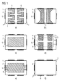
- FIGS. 1a to 1f show different layer views of a multilayer component which has a plurality of laterally juxtaposed stack of electrode layers 3. These are applied to common dielectric layers 2.
- the stacks of the electrode layers produce capacitances connected in parallel with the dielectric layers. Depending on the use of a suitable dielectric material, these can form a multilayer capacitor or a multilayer varistor.
- the multilayer component preferably has a plurality of external contacts 6, which can be arranged on different side surfaces 7 of the main body 1.
- the external contacts 6 can be realized as applied to the outer surface of the base body electrically conductive layers. According to one embodiment, these external contacts clasp the main body by being made into the edge region of the end faces of the main body 1.
- the external contacts do not necessarily have to be designed as layers; they may instead be designed in the form of a pencil with a circular or semicircular cross section. They may contain a material which is used for electrode layers of the multilayer component.
- the external contacts 6 may contain on their sides facing away from the main body a material which can be soldered with the lowest possible electrical contact resistance with the circuit board or with the mounting surface.
- FIG. 1a shows a plan view of a plane of the multilayer component in which a dielectric layer 2 is present.
- two meander-shaped resistor structures 5 are applied, which are each contacted at both ends with external contacts 6.
- the meander-shaped resistance paths 5 have opposite rectilinear resistance paths the advantage that high resistances can be achieved according to their relatively large lengths.
- FIG. 1b shows a plan view of a plane of the multilayer component in which two flat resistor structures 5 'are applied to a dielectric layer 2.
- the resistance structures are realized as resistance paths whose widths are greater in the edge region of the dielectric layer 2 than in the inner region. Based on their width, they have tapered sections. Such a construction has the advantage that contact resistances between the external contacts 6 and the resistance paths 5 'can be kept as low as possible.
- the resistance structures are in the uppermost position in relation to the switching elements described below. They may be applied to the surface of the base body 1 or integrated in the upper region of the base body. Also, resistance structures can be applied to both end faces of the base body. However, they can be integrated at any other level in the main body.
- the resistance structures may be provided with one or more passivation layers, in particular if they are arranged on the surface of the base body.
- the passivation layer preferably contains glass.
- Figure 1c shows a plan view of a plane of the multilayer component, which is preferably adjacent to the previously described resistance level in the stacking direction.
- a dielectric layer 2 is shown on which a floating shielding structure 4 is applied. This is due to the lack of contact with the external contacts or due to the lack of contact with any electrical contact as well as due to the laminating of the dielectric layer with an adjacent dielectric layer as a whole surrounded by dielectric material.
- the shielding structure 4 achieves an electromagnetic decoupling of the resistors or of the resistance structures of other parts, for example of layers underneath and electrically active structures applied to these layers, of the multilayer component.
- Figure 1d shows a plan view of a plane of the multilayer component in which four rectangular electrode layers 3 are arranged on a common dielectric layer 2.
- Each electrode layer 3 is connected at one end to an external contact 6, which is preferably arranged on a longitudinal side of the main body 1.
- the electrode layers may have different lengths and widths.
- Electrode layers 3, which are contacted with external contacts arranged on opposite side surfaces of the main body, can extend at different depths into the interior of the main body.
- Each stack of electrode layers and interposed dielectric layers may form a multilayer capacitor, depending on the use of a suitable dielectric.
- the figure can be seen accordingly that the multilayer component has four multilayer capacitors or varistors. However, more than this number of Learn Wegkondensatoren- or varistors may be formed, wherein a plurality of stacks of electrode layers in the longitudinal direction of the multilayer component may be arranged side by side, which may be arranged on common dielectric layers.
- the multilayer component with four multilayer capacitors in the manner described could have an end face of less than 3, preferably less than 2.5 mm 2 . It is preferred that the multilayer component has two resistance structures. In the case of, for example, eight multilayer capacitors, the multilayer component has, for example, an end face of less than 6, preferably less than 5.2 mm 2 . It has proven to be advantageous if the multilayer component in this case has four resistor structures which are shielded from one another by means of shielding structures.
- the number of resistor structures present in the multilayer component corresponds to half the number of multilayer capacitors or varistors of the multilayer component or half to the number of electrode layers applied to a common dielectric layer.
- FIG. 1d The structure shown by a dashed line of FIG Figure 1d represents a ground electrode 8, which is described in more detail with the following figure.
- Figure 1e shows a plan view of a plane of the multilayer component in which a force applied to a dielectric layer 2 ground electrode 8 is present. At both ends, this ground electrode is connected to an external contact 6.
- the ground electrode cooperates with the above-described multiple electrode layers and is preferably adjacent to them in the stacking direction. It can have a structure tapering from the inside out, in particular a cruciform one.
- the ground electrode can with several
- Multilayer capacitors or multilayer varistors cooperate or be guided by their respective stack.
- FIG. 1f shows a plane of the multilayer component in which only one dielectric layer is present. This could be arranged, for example, between dielectric layers with structured surfaces or, for example, on the underside of the base body.
- FIG. 2a shows a first layer structure of an electrical multilayer component, in which at an upper end face (based on the mounting of the multilayer component to a mounting surface) of the base body 1, a resistance structure 5 is arranged. This connects external contacts 6, the side of the body, including the edges, cover or clasp.
- a shielding structure 4 is integrated in the base body and adjacent to the resistance structure in comparison to other electrically active structures of the multilayer component, such as electrode layers or ground electrodes (but not dielectric layers).
- electrode layers or ground electrodes but not dielectric layers
- the shielding structure 4 with the exception of a dielectric layer, there are two electrode layers 3, which are arranged on a common dielectric layer. On the underlying level of the multilayer component, a ground electrode is present. Under this electrode layers 3 are again in the same arrangement as the electrode layers arranged above.
- Electrode layers 3 which are contacted with a common external contact 6 and cooperate with a counter electrode (in this case the ground electrode), form a first multilayer capacitor, if for the intermediate one dielectric layer, a capacitor ceramic is used, and a multilayer varistor when a varistor ceramic is used for the corresponding dielectric layer.
- a capacitor ceramic is used, and a multilayer varistor when a varistor ceramic is used for the corresponding dielectric layer.
- this example already shows two multilayer capacitors or multilayer varistors facing each other.
- FIG. 2b shows a further layer structure of an electrical multilayer component, in which at the top of a resistor structure 5 is integrated in the body.
- a first shielding structure 4 is arranged, followed by electrode layers 3 in an arrangement according to the preceding example.
- a ground electrode 8 is arranged as a counterelectrode, followed by further electrode layers 3.
- a second shielding structure 5 is integrated in the base body. This is followed by one or more dielectric layers 2 forming the lower outer surface of the main body.
- FIGS. 3a and 3b such as FIGS. 3b and 3c are to be considered together.
- Figure 3c schematically shows an arrangement of external contacts A to F of a multilayer component.
- the external contact A (see also Figure 3c ) is in FIG. 3a connected to In1, where In1 is an input line.
- the external contact C (see also Figure 3c ) is connected to O1 in Figure 3a, where 01 is an output line.
- the dielectric layers between the electrodes of the respective pairs of electrodes contain either a varistor ceramic or a capacitor ceramic.
- a capacitance C1 is formed between the first pair of electrode layers and the ground electrode.
- a further capacitance C2 is formed between the second pair of electrode layers, which is opposite to the first pair.
- the external contacts A and C or the input line ln1 and the output line 01 are connected to each other by means of a resistor structure 5, which is preferably arranged on the surface of the main body of the multilayer component.
- the resistance structure may, for example, have a value of between 90 and 110 ⁇ .
- a ⁇ -filter designed in this way acts as a low-pass filter in that capacitances C1 and C2 and the resistor 5 interact when the filter is subjected to voltages within a certain voltage value range.
- the low-pass filter optionally filters out interfering high-frequency signal components.
- the application of higher voltages to the multilayer component leads to the activation of a varistor effect when a varistor ceramic is used as the dielectric material between the electrodes of the first and the second electrode pair.
- the dielectric material which in itself has a high resistance value, becomes electrically conductive and conducts the signal associated with the high voltage via the ground electrode or via the external contact E connected to the ground electrode away from the multilayer component.
- a filter of the type described can be used for filtering out communication signals or noise signals and for dissipating overvoltages.
- the electrical multilayer component with its filter function is used, for example, as a hardware component in a mobile communication device and / or in a computer.
- the external contact B (see also Figure 3c ) is in FIG. 3b connected to ln2, where In2 is another input line.
- the external contact D (see also Figure 3c ) is in FIG. 3b connected to 02, where 02 is another output line.
- Input lines and output lines can be designed as printed conductors on a printed circuit board.
- the dielectric layers between the electrode layers of the respective electrode layer pairs contain either a varistor ceramic or a capacitor ceramic.
- a varistor ceramic or a capacitor ceramic.
- C3 Between the fourth pair of electrode layers, which is opposite to the third pair, further capacitance C4 is formed.
- the external contacts B and D are connected to one another by means of a resistor structure 5 contained in the multilayer component.
- the resistance structure may, for example, have a value of between 90 and 110 ⁇ .
- a thus formed second ⁇ -filter acts in the same manner as previously with the FIG. 3a described first ⁇ -filter, wherein by means of a varistor effect derived signals are not derived via the external contact E, but this time via the external contact F.
- First and third as well as second and fourth electrode pairs can be arranged laterally next to each other in the multilayer component.
- the resistor structures may contain the following materials: Rb0 2 , Bi 2 Ru 2 O 7 , C, Ti 2 N, LaB 6 .
- Preferred materials contained in electrode layers are Ag, Pd, Pt, AgPd alloys, AgPt alloys, Cu or Ni.
- the dielectric layers of the multilayer component may contain, as the capacitor ceramic, a material from the following capacitor ceramic classes: COG, X7R, Z5U, Y5V, HQM. These materials are particularly suitable when the electrical multilayer component is to have an EMI filter function.
- the dielectric layers of the multilayer component may contain ZnO-Bi or ZnO-Pr as varistor ceramic. These materials are particularly suitable if the electrical multilayer component is to have an EMI and / or an ESD filter function.
- FIG. 4 shows the insertion loss in dB of a multilayer component in a schematic way for injected signals whose frequencies are marked in GHz on the horizontal axis.
- the curve K1 shows the insertion loss of a multilayer component with a ⁇ -filter interconnection, the multilayer component having no shielding structure.
- the maximum insertion loss is about -35 dB at a frequency of 0.95 GHz.
- the curve K2 shows the insertion loss of a multilayer component with a ⁇ -filter interconnection, wherein the multilayer component has only one shielding structure, which is arranged between two stacks of a plurality of electrode layers.
- the maximum insertion loss is about -50 dB at a frequency of 1 GHz.
- the curve K3 shows the insertion loss of a multilayer component with a ⁇ -filter interconnection, the multilayer component having two shielding structures and two resistance structures shielded by the shielding structures.
- the maximum insertion loss is about -60 dB at a frequency of 1 GHz.
Landscapes
- Engineering & Computer Science (AREA)
- Power Engineering (AREA)
- Microelectronics & Electronic Packaging (AREA)
- Manufacturing & Machinery (AREA)
- Physics & Mathematics (AREA)
- Electromagnetism (AREA)
- Fixed Capacitors And Capacitor Manufacturing Machines (AREA)
- Thermistors And Varistors (AREA)
- Ceramic Capacitors (AREA)
- Shielding Devices Or Components To Electric Or Magnetic Fields (AREA)
Applications Claiming Priority (2)
| Application Number | Priority Date | Filing Date | Title |
|---|---|---|---|
| DE102007020783A DE102007020783A1 (de) | 2007-05-03 | 2007-05-03 | Elektrisches Vielschichtbauelement |
| PCT/EP2008/055264 WO2008135466A1 (de) | 2007-05-03 | 2008-04-29 | Elektrisches vielschichtbauelement mit elektrisch nicht kontaktierter abschirmstruktur |
Publications (2)
| Publication Number | Publication Date |
|---|---|
| EP2143117A1 EP2143117A1 (de) | 2010-01-13 |
| EP2143117B1 true EP2143117B1 (de) | 2011-08-03 |
Family
ID=39642620
Family Applications (1)
| Application Number | Title | Priority Date | Filing Date |
|---|---|---|---|
| EP08749865A Not-in-force EP2143117B1 (de) | 2007-05-03 | 2008-04-29 | Elektrisches vielschichtbauelement mit elektrisch nicht kontaktierter abschirmstruktur |
Country Status (8)
| Country | Link |
|---|---|
| US (1) | US8179210B2 (da) |
| EP (1) | EP2143117B1 (da) |
| JP (1) | JP5275338B2 (da) |
| KR (1) | KR101452540B1 (da) |
| AT (1) | ATE519208T1 (da) |
| DE (1) | DE102007020783A1 (da) |
| DK (1) | DK2143117T3 (da) |
| WO (1) | WO2008135466A1 (da) |
Families Citing this family (37)
| Publication number | Priority date | Publication date | Assignee | Title |
|---|---|---|---|---|
| DE102008062023A1 (de) | 2008-12-12 | 2010-06-17 | Epcos Ag | Elektrisches Vielschichtbauelement und Schaltungsanordnung damit |
| DE102009049077A1 (de) * | 2009-10-12 | 2011-04-14 | Epcos Ag | Elektrisches Vielschichtbauelement und Schaltungsanordnung |
| DE102011010611A1 (de) | 2011-02-08 | 2012-08-09 | Epcos Ag | Elektrisches Keramikbauelement mit elektrischer Abschirmung |
| JP5883244B2 (ja) * | 2011-07-12 | 2016-03-09 | 双信電機株式会社 | コンデンサモジュール |
| DE102012101606B4 (de) | 2011-10-28 | 2024-11-21 | Tdk Electronics Ag | ESD-Schutzbauelement und Bauelement mit einem ESD-Schutzbauelement und einer LED |
| KR102122935B1 (ko) * | 2013-03-29 | 2020-06-26 | 삼성전기주식회사 | 적층 세라믹 커패시터 및 그 제조 방법 |
| KR101994713B1 (ko) | 2013-04-22 | 2019-07-01 | 삼성전기주식회사 | 적층 세라믹 커패시터 및 그 실장 기판 |
| KR101514514B1 (ko) * | 2013-04-22 | 2015-04-22 | 삼성전기주식회사 | 적층 세라믹 커패시터 및 그 실장 기판 |
| KR101514532B1 (ko) * | 2013-07-22 | 2015-04-22 | 삼성전기주식회사 | 적층 세라믹 커패시터 |
| KR101608224B1 (ko) * | 2014-11-20 | 2016-04-14 | 주식회사 아모텍 | 감전보호소자 및 이를 구비한 휴대용 전자장치 |
| KR101608226B1 (ko) * | 2014-11-20 | 2016-04-14 | 주식회사 아모텍 | 감전보호소자 및 이를 구비한 휴대용 전자장치 |
| KR101578543B1 (ko) * | 2014-11-20 | 2015-12-17 | 주식회사 아모텍 | 감전보호소자 및 이를 구비한 휴대용 전자장치 |
| KR101578544B1 (ko) | 2014-11-20 | 2015-12-17 | 주식회사 아모텍 | 감전보호소자 및 이를 구비한 휴대용 전자장치 |
| WO2016122245A1 (ko) * | 2015-01-29 | 2016-08-04 | 주식회사 아모텍 | 감전보호기능이 내장된 휴대용 전자기기 |
| CN107211528B (zh) * | 2015-01-29 | 2020-08-11 | 阿莫泰克有限公司 | 内置有触电保护功能的便携式电子设备 |
| JP6554833B2 (ja) * | 2015-03-12 | 2019-08-07 | 株式会社村田製作所 | 複合電子部品および抵抗素子 |
| KR101978426B1 (ko) * | 2015-03-18 | 2019-05-14 | 주식회사 아모텍 | 감전보호소자 및 이를 구비하는 휴대용 전자장치 |
| WO2016178541A1 (ko) * | 2015-05-07 | 2016-11-10 | 주식회사 이노칩테크놀로지 | 감전 방지 소자 및 이를 구비하는 전자기기 |
| WO2016178528A1 (ko) * | 2015-05-07 | 2016-11-10 | 주식회사 이노칩테크놀로지 | 감전 방지 소자 및 이를 구비하는 전자기기 |
| WO2016178529A1 (ko) * | 2015-05-07 | 2016-11-10 | 주식회사 이노칩테크놀로지 | 감전 방지 소자 및 이를 구비하는 전자기기 |
| KR101808794B1 (ko) * | 2015-05-07 | 2018-01-18 | 주식회사 모다이노칩 | 적층체 소자 |
| WO2016178543A1 (ko) * | 2015-05-07 | 2016-11-10 | 주식회사 이노칩테크놀로지 | 감전 방지 소자 및 이를 구비하는 전자기기 |
| WO2017074088A1 (ko) * | 2015-10-28 | 2017-05-04 | 주식회사 아모텍 | 감전보호 장치 |
| DE102015120640B4 (de) | 2015-11-27 | 2025-12-04 | Tdk Electronics Ag | Vielschichtbauelement und Verfahren zur Herstellung eines Vielschichtbauelements |
| DE102016110742A1 (de) | 2016-06-10 | 2017-12-14 | Epcos Ag | Filterbauelement zur Filterung eines Störsignals |
| US10410794B2 (en) * | 2016-07-11 | 2019-09-10 | Kemet Electronics Corporation | Multilayer ceramic structure |
| DE102017115780A1 (de) * | 2017-07-13 | 2019-01-17 | Tdk Electronics Ag | Leuchtdiodenbauteil, Leuchtdiodenanordnung und Verfahren zur Herstellung eines Leuchtdiodenbauteils |
| US10161667B1 (en) * | 2017-11-15 | 2018-12-25 | Haier Us Appliance Solutions, Inc. | Refrigerator appliance having a defrost chamber |
| SG11202007528VA (en) | 2018-03-05 | 2020-09-29 | Avx Corp | Cascade varistor having improved energy handling capabilities |
| DE112019001153T5 (de) * | 2018-03-06 | 2020-12-03 | Avx Corporation | Mehrschichtiger Keramikkondensator mit Ultrabreitbandleistungsfähigkeit |
| DE102018116221B4 (de) * | 2018-07-04 | 2022-03-10 | Tdk Electronics Ag | Vielschichtvaristor mit feldoptimiertem Mikrogefüge und Modul aufweisend den Vielschichtvaristor |
| DE112019003625T5 (de) | 2018-07-18 | 2021-04-22 | Avx Corporation | Varistor-Passivierungsschicht und Verfahren zu ihrer Herstellung |
| WO2020132025A1 (en) | 2018-12-20 | 2020-06-25 | Avx Corporation | Multilayer filter including a return signal reducing protrusion |
| US11336249B2 (en) | 2018-12-20 | 2022-05-17 | KYOCERA AVX Components Corporation | Multilayer filter including a capacitor connected with at least two vias |
| JP7288056B2 (ja) | 2018-12-20 | 2023-06-06 | キョーセラ・エイブイエックス・コンポーネンツ・コーポレーション | 高精度インダクタを含む多層電子デバイス |
| CN113228409B (zh) * | 2018-12-20 | 2022-05-27 | 京瓷Avx元器件公司 | 包括具有精确控制电容面积的电容器的多层电子装置 |
| WO2020132011A1 (en) | 2018-12-20 | 2020-06-25 | Avx Corporation | High frequency multilayer filter |
Family Cites Families (32)
| Publication number | Priority date | Publication date | Assignee | Title |
|---|---|---|---|---|
| US4302362A (en) * | 1979-01-23 | 1981-11-24 | E. I. Du Pont De Nemours And Company | Stable pyrochlore resistor compositions |
| US4460497A (en) * | 1983-02-18 | 1984-07-17 | Westinghouse Electric Corp. | Voltage stable nonlinear resistor containing minor amounts of aluminum and selected alkali metal additives |
| JPH0630292B2 (ja) * | 1986-05-23 | 1994-04-20 | 株式会社村田製作所 | 複合部品の製造方法 |
| JPH05275958A (ja) * | 1992-03-25 | 1993-10-22 | Murata Mfg Co Ltd | ノイズフィルタ |
| JPH08265083A (ja) * | 1995-03-24 | 1996-10-11 | Mitsubishi Materials Corp | チップ型低域フィルタ |
| JPH08273970A (ja) * | 1995-03-29 | 1996-10-18 | Murata Mfg Co Ltd | 積層セラミック電子部品 |
| JP3631341B2 (ja) * | 1996-10-18 | 2005-03-23 | Tdk株式会社 | 積層型複合機能素子およびその製造方法 |
| US6201439B1 (en) * | 1997-09-17 | 2001-03-13 | Matsushita Electric Industrial Co., Ltd. | Power splitter/ combiner circuit, high power amplifier and balun circuit |
| JP4257711B2 (ja) | 1998-02-25 | 2009-04-22 | 日本碍子株式会社 | 電子部品用接合剤および電子部品 |
| JP2970652B1 (ja) * | 1998-05-22 | 1999-11-02 | 松下電器産業株式会社 | 積層セラミック部品およびその製造方法 |
| JP2000164461A (ja) * | 1998-11-25 | 2000-06-16 | Sony Corp | チップ部品 |
| DE19931056B4 (de) | 1999-07-06 | 2005-05-19 | Epcos Ag | Vielschichtvaristor niedriger Kapazität |
| JP2001118731A (ja) * | 1999-10-19 | 2001-04-27 | Murata Mfg Co Ltd | チップ型複合電子部品およびその製造方法 |
| JP2001307910A (ja) * | 2000-04-25 | 2001-11-02 | Tdk Corp | 積層電子部品アレイ |
| DE10026258B4 (de) | 2000-05-26 | 2004-03-25 | Epcos Ag | Keramisches Material, keramisches Bauelement mit dem keramischen Material und Verwendung des keramischen Bauelements |
| JP3933849B2 (ja) * | 2000-06-30 | 2007-06-20 | 松下電器産業株式会社 | 電子部品類集合体を用いた携帯機器 |
| JP2002033634A (ja) | 2000-07-18 | 2002-01-31 | Rohm Co Ltd | Lcフィルタ |
| JP2002118033A (ja) | 2000-10-06 | 2002-04-19 | Murata Mfg Co Ltd | 複合電子部品 |
| DE10064445A1 (de) * | 2000-12-22 | 2002-07-11 | Epcos Ag | Elektrisches Vielschichtbauelement und Anordnung mit dem Bauelement |
| KR100864917B1 (ko) | 2001-11-03 | 2008-10-22 | 엘지디스플레이 주식회사 | 액정표시장치의 데이터 구동 장치 및 방법 |
| DE10224565A1 (de) | 2002-06-03 | 2003-12-18 | Epcos Ag | Elektrisches Vielschichtbauelement und Schaltungsanordnung |
| DE10356498A1 (de) * | 2003-12-03 | 2005-07-07 | Epcos Ag | Elektrisches Bauelement und Schaltungsanordnung |
| KR20050080823A (ko) | 2004-02-11 | 2005-08-18 | 이경재 | 발광기능을 부가한 엑세서리 |
| DE102004045009B4 (de) | 2004-09-16 | 2008-03-27 | Epcos Ag | Elektrisches Bauelement und dessen Verwendung |
| KR20060031943A (ko) * | 2004-10-11 | 2006-04-14 | 삼성전기주식회사 | 바리스터-lc필터 겸용 복합소자 |
| JP4507837B2 (ja) * | 2004-11-08 | 2010-07-21 | パナソニック株式会社 | 積層型電子部品の製造方法 |
| JP4270395B2 (ja) * | 2005-03-28 | 2009-05-27 | Tdk株式会社 | 積層セラミック電子部品 |
| JP4899356B2 (ja) * | 2005-06-30 | 2012-03-21 | 富士通オプティカルコンポーネンツ株式会社 | 光変調器 |
| DE102005050638B4 (de) | 2005-10-20 | 2020-07-16 | Tdk Electronics Ag | Elektrisches Bauelement |
| JP4586760B2 (ja) * | 2006-03-29 | 2010-11-24 | Tdk株式会社 | ローパスフィルタ及びローパスフィルタアレイ |
| DE102007031510A1 (de) * | 2007-07-06 | 2009-01-08 | Epcos Ag | Elektrisches Vielschichtbauelement |
| US7737818B2 (en) * | 2007-08-07 | 2010-06-15 | Delphi Technologies, Inc. | Embedded resistor and capacitor circuit and method of fabricating same |
-
2007
- 2007-05-03 DE DE102007020783A patent/DE102007020783A1/de not_active Ceased
-
2008
- 2008-04-29 AT AT08749865T patent/ATE519208T1/de active
- 2008-04-29 KR KR1020097023756A patent/KR101452540B1/ko not_active Expired - Fee Related
- 2008-04-29 JP JP2010504734A patent/JP5275338B2/ja not_active Expired - Fee Related
- 2008-04-29 DK DK08749865.5T patent/DK2143117T3/da active
- 2008-04-29 EP EP08749865A patent/EP2143117B1/de not_active Not-in-force
- 2008-04-29 WO PCT/EP2008/055264 patent/WO2008135466A1/de not_active Ceased
-
2009
- 2009-11-03 US US12/611,290 patent/US8179210B2/en not_active Expired - Fee Related
Also Published As
| Publication number | Publication date |
|---|---|
| DK2143117T3 (da) | 2011-11-21 |
| EP2143117A1 (de) | 2010-01-13 |
| DE102007020783A1 (de) | 2008-11-06 |
| US20100109804A1 (en) | 2010-05-06 |
| KR20100019981A (ko) | 2010-02-19 |
| US8179210B2 (en) | 2012-05-15 |
| JP2010526429A (ja) | 2010-07-29 |
| ATE519208T1 (de) | 2011-08-15 |
| KR101452540B1 (ko) | 2014-10-21 |
| WO2008135466A1 (de) | 2008-11-13 |
| JP5275338B2 (ja) | 2013-08-28 |
Similar Documents
| Publication | Publication Date | Title |
|---|---|---|
| EP2143117B1 (de) | Elektrisches vielschichtbauelement mit elektrisch nicht kontaktierter abschirmstruktur | |
| EP2174328B1 (de) | elektrisches Vielschichtbauelement mit einem Widerstand und einer Entkopplungsschicht | |
| EP2201585B1 (de) | Elektrisches vielschichtbauelement | |
| EP1350257B1 (de) | Elektrisches vielschichtbauelement und entstörschaltung mit dem bauelement | |
| DE10313891A1 (de) | Elektrisches Vielschichtbauelement | |
| EP1369880B1 (de) | Elektrisches Vielschichtbauelement und Schaltungsanordnung | |
| WO2003028045A2 (de) | Elektrisches vielschichtbauelement | |
| WO2010066848A1 (de) | Elektrisches vielschichtbauelement und schaltungsanordnung damit | |
| DE102007013751B4 (de) | Tiefpassfilter und Tiefpassfilter-Anordnung | |
| DE102004010001A1 (de) | Elektrisches Bauelement und schaltungsanordnung mit dem Bauelement | |
| EP1369881B1 (de) | Elektrisches Vielschichtbauelement | |
| DE102005028498B4 (de) | Elektrisches Vielschichtbauelement | |
| EP1391898B1 (de) | Elektrisches Vielschichtbauelement | |
| EP1817778B1 (de) | Vielschichtbauelement mit mehreren varistoren unterschiedlicher kapazität als esd-schutzelement | |
| DE102004016146A1 (de) | Elektrische Funktionseinheit | |
| DE102007044453A1 (de) | Elektrisches Vielschichtbauelement | |
| WO2004025831A1 (de) | Mehrfachresonanzfilter | |
| EP1880399A2 (de) | Elektrisches durchführungsbauelement und verfahren zu dessen herstellung | |
| EP2246866B1 (de) | Elektrisches Bauelement und Schaltungsanordnung | |
| EP1560235B1 (de) | Elektrisches Vielschichtbauelement | |
| DE112020005494T5 (de) | Varistor | |
| WO2003009311A1 (de) | Elektrokeramisches bauelement | |
| EP1911052B1 (de) | Elektrisches bauelement |
Legal Events
| Date | Code | Title | Description |
|---|---|---|---|
| PUAI | Public reference made under article 153(3) epc to a published international application that has entered the european phase |
Free format text: ORIGINAL CODE: 0009012 |
|
| 17P | Request for examination filed |
Effective date: 20091026 |
|
| AK | Designated contracting states |
Kind code of ref document: A1 Designated state(s): AT BE BG CH CY CZ DE DK EE ES FI FR GB GR HR HU IE IS IT LI LT LU LV MC MT NL NO PL PT RO SE SI SK TR |
|
| DAX | Request for extension of the european patent (deleted) | ||
| 17Q | First examination report despatched |
Effective date: 20100922 |
|
| GRAP | Despatch of communication of intention to grant a patent |
Free format text: ORIGINAL CODE: EPIDOSNIGR1 |
|
| GRAS | Grant fee paid |
Free format text: ORIGINAL CODE: EPIDOSNIGR3 |
|
| GRAA | (expected) grant |
Free format text: ORIGINAL CODE: 0009210 |
|
| AK | Designated contracting states |
Kind code of ref document: B1 Designated state(s): AT BE BG CH CY CZ DE DK EE ES FI FR GB GR HR HU IE IS IT LI LT LU LV MC MT NL NO PL PT RO SE SI SK TR |
|
| REG | Reference to a national code |
Ref country code: GB Ref legal event code: FG4D Free format text: NOT ENGLISH |
|
| REG | Reference to a national code |
Ref country code: CH Ref legal event code: EP |
|
| REG | Reference to a national code |
Ref country code: IE Ref legal event code: FG4D Free format text: LANGUAGE OF EP DOCUMENT: GERMAN |
|
| REG | Reference to a national code |
Ref country code: DE Ref legal event code: R096 Ref document number: 502008004405 Country of ref document: DE Effective date: 20110929 |
|
| REG | Reference to a national code |
Ref country code: DK Ref legal event code: T3 |
|
| REG | Reference to a national code |
Ref country code: SE Ref legal event code: TRGR |
|
| REG | Reference to a national code |
Ref country code: NL Ref legal event code: VDEP Effective date: 20110803 |
|
| LTIE | Lt: invalidation of european patent or patent extension |
Effective date: 20110803 |
|
| PG25 | Lapsed in a contracting state [announced via postgrant information from national office to epo] |
Ref country code: NL Free format text: LAPSE BECAUSE OF FAILURE TO SUBMIT A TRANSLATION OF THE DESCRIPTION OR TO PAY THE FEE WITHIN THE PRESCRIBED TIME-LIMIT Effective date: 20110803 Ref country code: NO Free format text: LAPSE BECAUSE OF FAILURE TO SUBMIT A TRANSLATION OF THE DESCRIPTION OR TO PAY THE FEE WITHIN THE PRESCRIBED TIME-LIMIT Effective date: 20111103 Ref country code: IS Free format text: LAPSE BECAUSE OF FAILURE TO SUBMIT A TRANSLATION OF THE DESCRIPTION OR TO PAY THE FEE WITHIN THE PRESCRIBED TIME-LIMIT Effective date: 20111203 Ref country code: LT Free format text: LAPSE BECAUSE OF FAILURE TO SUBMIT A TRANSLATION OF THE DESCRIPTION OR TO PAY THE FEE WITHIN THE PRESCRIBED TIME-LIMIT Effective date: 20110803 Ref country code: HR Free format text: LAPSE BECAUSE OF FAILURE TO SUBMIT A TRANSLATION OF THE DESCRIPTION OR TO PAY THE FEE WITHIN THE PRESCRIBED TIME-LIMIT Effective date: 20110803 Ref country code: PT Free format text: LAPSE BECAUSE OF FAILURE TO SUBMIT A TRANSLATION OF THE DESCRIPTION OR TO PAY THE FEE WITHIN THE PRESCRIBED TIME-LIMIT Effective date: 20111205 |
|
| PG25 | Lapsed in a contracting state [announced via postgrant information from national office to epo] |
Ref country code: GR Free format text: LAPSE BECAUSE OF FAILURE TO SUBMIT A TRANSLATION OF THE DESCRIPTION OR TO PAY THE FEE WITHIN THE PRESCRIBED TIME-LIMIT Effective date: 20111104 Ref country code: SI Free format text: LAPSE BECAUSE OF FAILURE TO SUBMIT A TRANSLATION OF THE DESCRIPTION OR TO PAY THE FEE WITHIN THE PRESCRIBED TIME-LIMIT Effective date: 20110803 Ref country code: LV Free format text: LAPSE BECAUSE OF FAILURE TO SUBMIT A TRANSLATION OF THE DESCRIPTION OR TO PAY THE FEE WITHIN THE PRESCRIBED TIME-LIMIT Effective date: 20110803 Ref country code: PL Free format text: LAPSE BECAUSE OF FAILURE TO SUBMIT A TRANSLATION OF THE DESCRIPTION OR TO PAY THE FEE WITHIN THE PRESCRIBED TIME-LIMIT Effective date: 20110803 Ref country code: CY Free format text: LAPSE BECAUSE OF FAILURE TO SUBMIT A TRANSLATION OF THE DESCRIPTION OR TO PAY THE FEE WITHIN THE PRESCRIBED TIME-LIMIT Effective date: 20110803 |
|
| REG | Reference to a national code |
Ref country code: IE Ref legal event code: FD4D |
|
| PG25 | Lapsed in a contracting state [announced via postgrant information from national office to epo] |
Ref country code: SK Free format text: LAPSE BECAUSE OF FAILURE TO SUBMIT A TRANSLATION OF THE DESCRIPTION OR TO PAY THE FEE WITHIN THE PRESCRIBED TIME-LIMIT Effective date: 20110803 Ref country code: IE Free format text: LAPSE BECAUSE OF FAILURE TO SUBMIT A TRANSLATION OF THE DESCRIPTION OR TO PAY THE FEE WITHIN THE PRESCRIBED TIME-LIMIT Effective date: 20110803 Ref country code: CZ Free format text: LAPSE BECAUSE OF FAILURE TO SUBMIT A TRANSLATION OF THE DESCRIPTION OR TO PAY THE FEE WITHIN THE PRESCRIBED TIME-LIMIT Effective date: 20110803 |
|
| PG25 | Lapsed in a contracting state [announced via postgrant information from national office to epo] |
Ref country code: RO Free format text: LAPSE BECAUSE OF FAILURE TO SUBMIT A TRANSLATION OF THE DESCRIPTION OR TO PAY THE FEE WITHIN THE PRESCRIBED TIME-LIMIT Effective date: 20110803 Ref country code: IT Free format text: LAPSE BECAUSE OF FAILURE TO SUBMIT A TRANSLATION OF THE DESCRIPTION OR TO PAY THE FEE WITHIN THE PRESCRIBED TIME-LIMIT Effective date: 20110803 Ref country code: EE Free format text: LAPSE BECAUSE OF FAILURE TO SUBMIT A TRANSLATION OF THE DESCRIPTION OR TO PAY THE FEE WITHIN THE PRESCRIBED TIME-LIMIT Effective date: 20110803 |
|
| PLBE | No opposition filed within time limit |
Free format text: ORIGINAL CODE: 0009261 |
|
| STAA | Information on the status of an ep patent application or granted ep patent |
Free format text: STATUS: NO OPPOSITION FILED WITHIN TIME LIMIT |
|
| 26N | No opposition filed |
Effective date: 20120504 |
|
| REG | Reference to a national code |
Ref country code: DE Ref legal event code: R097 Ref document number: 502008004405 Country of ref document: DE Effective date: 20120504 |
|
| BERE | Be: lapsed |
Owner name: EPCOS A.G. Effective date: 20120430 |
|
| PG25 | Lapsed in a contracting state [announced via postgrant information from national office to epo] |
Ref country code: MC Free format text: LAPSE BECAUSE OF NON-PAYMENT OF DUE FEES Effective date: 20120430 |
|
| REG | Reference to a national code |
Ref country code: CH Ref legal event code: PL |
|
| PG25 | Lapsed in a contracting state [announced via postgrant information from national office to epo] |
Ref country code: CH Free format text: LAPSE BECAUSE OF NON-PAYMENT OF DUE FEES Effective date: 20120430 Ref country code: LI Free format text: LAPSE BECAUSE OF NON-PAYMENT OF DUE FEES Effective date: 20120430 Ref country code: BE Free format text: LAPSE BECAUSE OF NON-PAYMENT OF DUE FEES Effective date: 20120430 |
|
| PG25 | Lapsed in a contracting state [announced via postgrant information from national office to epo] |
Ref country code: ES Free format text: LAPSE BECAUSE OF FAILURE TO SUBMIT A TRANSLATION OF THE DESCRIPTION OR TO PAY THE FEE WITHIN THE PRESCRIBED TIME-LIMIT Effective date: 20111114 |
|
| PG25 | Lapsed in a contracting state [announced via postgrant information from national office to epo] |
Ref country code: BG Free format text: LAPSE BECAUSE OF FAILURE TO SUBMIT A TRANSLATION OF THE DESCRIPTION OR TO PAY THE FEE WITHIN THE PRESCRIBED TIME-LIMIT Effective date: 20111103 |
|
| PG25 | Lapsed in a contracting state [announced via postgrant information from national office to epo] |
Ref country code: MT Free format text: LAPSE BECAUSE OF FAILURE TO SUBMIT A TRANSLATION OF THE DESCRIPTION OR TO PAY THE FEE WITHIN THE PRESCRIBED TIME-LIMIT Effective date: 20110803 |
|
| PG25 | Lapsed in a contracting state [announced via postgrant information from national office to epo] |
Ref country code: TR Free format text: LAPSE BECAUSE OF FAILURE TO SUBMIT A TRANSLATION OF THE DESCRIPTION OR TO PAY THE FEE WITHIN THE PRESCRIBED TIME-LIMIT Effective date: 20110803 |
|
| PG25 | Lapsed in a contracting state [announced via postgrant information from national office to epo] |
Ref country code: LU Free format text: LAPSE BECAUSE OF NON-PAYMENT OF DUE FEES Effective date: 20120429 |
|
| REG | Reference to a national code |
Ref country code: AT Ref legal event code: MM01 Ref document number: 519208 Country of ref document: AT Kind code of ref document: T Effective date: 20130429 |
|
| PG25 | Lapsed in a contracting state [announced via postgrant information from national office to epo] |
Ref country code: HU Free format text: LAPSE BECAUSE OF FAILURE TO SUBMIT A TRANSLATION OF THE DESCRIPTION OR TO PAY THE FEE WITHIN THE PRESCRIBED TIME-LIMIT Effective date: 20080429 |
|
| PG25 | Lapsed in a contracting state [announced via postgrant information from national office to epo] |
Ref country code: AT Free format text: LAPSE BECAUSE OF NON-PAYMENT OF DUE FEES Effective date: 20130429 |
|
| REG | Reference to a national code |
Ref country code: FR Ref legal event code: PLFP Year of fee payment: 9 |
|
| REG | Reference to a national code |
Ref country code: FR Ref legal event code: PLFP Year of fee payment: 10 |
|
| REG | Reference to a national code |
Ref country code: FR Ref legal event code: PLFP Year of fee payment: 11 |
|
| REG | Reference to a national code |
Ref country code: DE Ref legal event code: R082 Ref document number: 502008004405 Country of ref document: DE Representative=s name: EPPING HERMANN FISCHER PATENTANWALTSGESELLSCHA, DE Ref country code: DE Ref legal event code: R081 Ref document number: 502008004405 Country of ref document: DE Owner name: TDK ELECTRONICS AG, DE Free format text: FORMER OWNER: EPCOS AG, 81669 MUENCHEN, DE |
|
| PGFP | Annual fee paid to national office [announced via postgrant information from national office to epo] |
Ref country code: FI Payment date: 20190416 Year of fee payment: 12 Ref country code: DK Payment date: 20190425 Year of fee payment: 12 |
|
| PGFP | Annual fee paid to national office [announced via postgrant information from national office to epo] |
Ref country code: ES Payment date: 20190503 Year of fee payment: 11 |
|
| PGFP | Annual fee paid to national office [announced via postgrant information from national office to epo] |
Ref country code: FR Payment date: 20200421 Year of fee payment: 13 |
|
| REG | Reference to a national code |
Ref country code: FI Ref legal event code: MAE |
|
| REG | Reference to a national code |
Ref country code: DK Ref legal event code: EBP Effective date: 20200430 |
|
| PG25 | Lapsed in a contracting state [announced via postgrant information from national office to epo] |
Ref country code: FI Free format text: LAPSE BECAUSE OF NON-PAYMENT OF DUE FEES Effective date: 20200429 Ref country code: SE Free format text: LAPSE BECAUSE OF NON-PAYMENT OF DUE FEES Effective date: 20200430 |
|
| PG25 | Lapsed in a contracting state [announced via postgrant information from national office to epo] |
Ref country code: DK Free format text: LAPSE BECAUSE OF NON-PAYMENT OF DUE FEES Effective date: 20200430 |
|
| PG25 | Lapsed in a contracting state [announced via postgrant information from national office to epo] |
Ref country code: FR Free format text: LAPSE BECAUSE OF NON-PAYMENT OF DUE FEES Effective date: 20210430 |
|
| PGFP | Annual fee paid to national office [announced via postgrant information from national office to epo] |
Ref country code: GB Payment date: 20220425 Year of fee payment: 15 Ref country code: DE Payment date: 20220426 Year of fee payment: 15 |
|
| REG | Reference to a national code |
Ref country code: DE Ref legal event code: R119 Ref document number: 502008004405 Country of ref document: DE |
|
| GBPC | Gb: european patent ceased through non-payment of renewal fee |
Effective date: 20230429 |
|
| PG25 | Lapsed in a contracting state [announced via postgrant information from national office to epo] |
Ref country code: GB Free format text: LAPSE BECAUSE OF NON-PAYMENT OF DUE FEES Effective date: 20230429 |
|
| PG25 | Lapsed in a contracting state [announced via postgrant information from national office to epo] |
Ref country code: GB Free format text: LAPSE BECAUSE OF NON-PAYMENT OF DUE FEES Effective date: 20230429 Ref country code: DE Free format text: LAPSE BECAUSE OF NON-PAYMENT OF DUE FEES Effective date: 20231103 |