EP2143231B1 - Vorrichtung zur rückgewinnung des taktes und digitaler daten ohne extenre regelung - Google Patents
Vorrichtung zur rückgewinnung des taktes und digitaler daten ohne extenre regelung Download PDFInfo
- Publication number
- EP2143231B1 EP2143231B1 EP08787917.7A EP08787917A EP2143231B1 EP 2143231 B1 EP2143231 B1 EP 2143231B1 EP 08787917 A EP08787917 A EP 08787917A EP 2143231 B1 EP2143231 B1 EP 2143231B1
- Authority
- EP
- European Patent Office
- Prior art keywords
- signal
- input
- phase
- clock
- circuit
- Prior art date
- Legal status (The legal status is an assumption and is not a legal conclusion. Google has not performed a legal analysis and makes no representation as to the accuracy of the status listed.)
- Active
Links
Images






Classifications
-
- H—ELECTRICITY
- H04—ELECTRIC COMMUNICATION TECHNIQUE
- H04L—TRANSMISSION OF DIGITAL INFORMATION, e.g. TELEGRAPHIC COMMUNICATION
- H04L7/00—Arrangements for synchronising receiver with transmitter
- H04L7/02—Speed or phase control by the received code signals, the signals containing no special synchronisation information
- H04L7/027—Speed or phase control by the received code signals, the signals containing no special synchronisation information extracting the synchronising or clock signal from the received signal spectrum, e.g. by using a resonant or bandpass circuit
-
- H—ELECTRICITY
- H03—ELECTRONIC CIRCUITRY
- H03L—AUTOMATIC CONTROL, STARTING, SYNCHRONISATION OR STABILISATION OF GENERATORS OF ELECTRONIC OSCILLATIONS OR PULSES
- H03L7/00—Automatic control of frequency or phase; Synchronisation
- H03L7/06—Automatic control of frequency or phase; Synchronisation using a reference signal applied to a frequency- or phase-locked loop
- H03L7/08—Details of the phase-locked loop
- H03L7/083—Details of the phase-locked loop the reference signal being additionally directly applied to the generator
-
- H—ELECTRICITY
- H04—ELECTRIC COMMUNICATION TECHNIQUE
- H04L—TRANSMISSION OF DIGITAL INFORMATION, e.g. TELEGRAPHIC COMMUNICATION
- H04L7/00—Arrangements for synchronising receiver with transmitter
- H04L7/02—Speed or phase control by the received code signals, the signals containing no special synchronisation information
- H04L7/027—Speed or phase control by the received code signals, the signals containing no special synchronisation information extracting the synchronising or clock signal from the received signal spectrum, e.g. by using a resonant or bandpass circuit
- H04L7/0276—Self-sustaining, e.g. by tuned delay line and a feedback path to a logical gate
-
- H—ELECTRICITY
- H04—ELECTRIC COMMUNICATION TECHNIQUE
- H04L—TRANSMISSION OF DIGITAL INFORMATION, e.g. TELEGRAPHIC COMMUNICATION
- H04L7/00—Arrangements for synchronising receiver with transmitter
- H04L7/02—Speed or phase control by the received code signals, the signals containing no special synchronisation information
- H04L7/033—Speed or phase control by the received code signals, the signals containing no special synchronisation information using the transitions of the received signal to control the phase of the synchronising-signal-generating means, e.g. using a phase-locked loop
Definitions
- the invention relates to a device for extracting a clock and digital data from a baseband serial signal, said received signal, representative of the digital data, and coded with a clock signal having a frequency of bit clock fsr corresponding at least substantially to a nominal frequency fn.
- the most usual solution for producing such a clock and data extraction device consists in using circuits comprising at least one phase-locked loop, called PLL, which mainly comprises, at the output of a circuit generating pulses corresponding to the edges of the received signal, a phase comparator delivering a reference signal to a voltage controlled oscillator, VCO, via a loop filter.
- the VCO provides an internal clock signal to a decision latch, constituting a sampling circuit that extracts data from the received signal.
- DLL delay locked loop
- FR 2838265 has proposed a solution consisting in using an injection oscillator, that is to say an oscillator locked in injection on the frequency of edges of the signal received, in an open-loop circuit.
- the injection oscillator is a negative resistance oscillator using a coupled pair of MOS transistors, and receives a synchronization pulse signal clocked at the bit clock frequency fsr of the received signal, this pulse signal being emitted by a current pulse generator.
- This oscillator locked in injection having a frequency of free oscillations fos, has the ability to lock on the pulse signal if the frequency of the latter is in its operating range, called the capture range. It then provides a clock signal whose frequency corresponds exactly to the clock bit frequency fsr.
- US 6317008 also discloses a clock and data extraction device comprising an injection-locked oscillator, which does not include a phase-locked loop and requires, like all the documents providing for the use of such a locked oscillator in injection , a control voltage of the oscillator locked in injection and a manual individual calibration according to each application.
- the hooking range of the circuit is in all cases very low.
- the signal supplied by the pulse generator supplying both the oscillator and the phase comparator is not optimized for these two circuits simultaneously, so that an external manual adjustment of the natural frequency of the Oscillator is needed which is not compatible with industrial scale operation.
- a phase comparator of simple realization for example of the exclusive OR type, while preserving a sufficient capture range and a low sensitivity to duty cycle variations of the received signals.
- FR 2838265 a also proposed to solve this phase shift problem by providing decision logic for selecting a value among different values provided by a plurality of sampling flip-flops shifted at distinct offset times with respect to the pulses of the receive clock signal . It turns out that in practice this solution is not really effective in all situations.
- this resonant circuit is not compatible with any input data signals, especially when they have significant periods without transitions.
- the clock and data extraction circuits must be able to support 5-bit periods without transitions, and with code 8B / 12B they have to support 11-bit periods without transitions.
- the device described in this document is not capable of such performance. To overcome this problem, given the state of the art previously mentioned, only a device based on a PLL would be possible, but with the aforementioned disadvantages.
- the invention therefore aims to propose such a solution.
- the inventors have indeed found that it is possible, with a specific architecture, to propose for the first time a clock extraction device and data that has these qualities, and in particular that is very simple, " auto tuned ", with a wide snap range and a negligible bit error rate.
- the invention aims in particular to provide such a device which is compatible with the use of an exclusive OR type phase comparator in the phase control loop.
- the invention also aims at providing such a device that is insensitive to the variation in quality of the received signals, and in particular that is compatible with signals that may have a variable transition density and noise.
- the terms "input” and “output” of a component denote a connection terminal or a set of connection terminals receiving or, respectively, delivering a signal.
- the signal applied to an input or delivered by an output may therefore be, unless otherwise specified, both a serial signal and a parallel signal, and may consist of a single channel or of several channels (in particular in the case of a differential type architecture).
- the phase pulse generator delivering pulses adapted to the phase-locked loop, the capture range of this phase-locked loop, and therefore the clock extraction circuit, is large enough for this
- the clock extraction circuit may be free from any external manual adjustment, and in particular from any adjustment of the frequency of free oscillations fos of the locked oscillator in injection.
- the phase-pulse generator makes it possible to decorrelate the phase-locked loop with respect to the received signal, whatever the characteristics of the latter (type of transmission coding, electrical and temporal characteristics).
- the pulses delivered by the phase pulse generator makes it possible to dispense with the real waveform of the received signal while avoiding any amplitude noise, and by straightening the rising and falling edges.
- these pulses are calibrated in duration and amplitude so as to be particularly optimized and adapted to the phase-locked loop, in particular the phase comparator contained in this loop.
- these pulses are voltage pulses and may be calibrated to have a predetermined specific duty cycle and / or a predetermined specific magnitude level. This calibration in duration and in amplitude carried out within the device according to the invention makes it possible to control the range frequency of the received signal on which the phase control can be realized, and thus to obtain a much higher capture range with the devices of the state of the prior art.
- a device is capable of adapting in real time (that is to say with a very low latency of a few bits in the worst situation and generally less than a bit duration) to changes in the frequency of the signal received over a wide range of frequencies.
- the invention thus makes it possible to provide decisive advantages in the design of clock extraction devices and digital data devices, by allowing an operation on an industrial scale of a circuit whose operation is based on a locked oscillator. injection.
- a device according to the invention is, because of its overall architecture, completely autonomous, that is to say does not require any manual external adjustment or other, nor any calibration. Thus, a device according to the invention is free from any external manual adjustment means. In addition, this autonomy is obtained with great simplicity of realization.
- a device In a device according to the invention it is possible to use an extremely simple phase comparator, for example of exclusive OR type, of reduced consumption and allowing a rise in frequency, the phase servocontrol loop having a sufficient capture range extended so that no external adjustment is necessary.
- a device also does not require the presence of an external frequency reference, and this contrary to a traditional PLL.
- the startup synchronization preamble can be reduced considerably, generally to a few bits. Because of its great simplicity, the architecture of a device according to the invention allows its realization with a very low number of elementary components with low energy consumption (thus a reduced surface and a lower consumption).
- a device according to the invention can also be designed without requiring the intervention of a designer with a great know-how in the design of clock and data extractor circuits (unlike prior devices based PLL in which he in particular, it is very difficult to produce a phase / frequency comparator operating at high frequency). It is also possible, with a device according to the invention of simple design, to achieve transmission speeds close to the limits offered by semiconductor technology. In particular, it is possible to achieve significantly higher transmission rates than with previous circuits based on PLL or DLL. In addition, it is possible to produce a device according to the invention with any semiconductor technology (CMOS, bipolar, SiGe, etc.).
- bit error rate of a device is less sensitive to noise on the received signal, and the coding of the data has an expansion rate similar to that of a traditional PLL, that is to say much lower than that required by a DLL.
- a device according to the invention is intrinsically very insensitive to transient events that can be triggered by ionizing particles once the oscillator is in locked mode.
- a device according to the invention is particularly advantageous for nuclear, aeronautical, military and space applications.
- a device according to the invention being insensitive, at ground level, atmospheric neutrons, alpha particles and parasitic noise intrinsic to submicron technologies, is also particularly advantageous in other industrial applications in which these phenomena are present.
- the natural frequency fos of the oscillator is always equal to the bit clock frequency fsr of reception clock signal, and the phase difference between the clock signal delivered by the oscillator and the received signal is fixed. Since all the other elements constituting the device can cause a constant phase shift between the two inputs of the sampling circuit, it is possible to determine the constant structural phase differential delay between these two inputs of the sampling circuit. Therefore, it suffices to provide one (or more) phase-shifter circuit (s) to ensure phase alignment between the two inputs of the sampling circuit, without requiring any external adjustment, so that the device according to the invention can operate autonomously and stable with a wide range of capture.
- phase shifter (s) is (are) provided (s) in addition to the possible phase shifting circuit sometimes necessarily provided at the input of a circuit such that a phase comparator, to compensate for the phase shifts introduced by certain architectures of this type of circuit (see for example GB 2113929 which provides a delay circuit to ensure that the output signal of the phase comparator is zero when the signals at the input are in phase).
- phase-shifting circuit necessary for the operation of a phase comparator that it supplies is functionally different from the phase-shifter circuit (s) of a device according to the invention, the function of which is to introduce a additional phase shift to compensate for the total phase shift between the two inputs of the sampling circuit.
- the invention makes it possible, for the first time, to obtain a completely autonomous and stable data extraction and clock circuit that can be used on an industrial scale in many applications.
- the phase-locked loop comprises a phase-comparator circuit comprising a first input connected to the clock output, a second input connected to the output of the phase-pulse generator, and an output delivering a signal-in particular a voltage-analog signal whose amplitude is a function of the phase difference between the first input and the second input, and in that the pulse generator phase detector is adapted to generate a pulse signal with a duration and an amplitude of the pulses adapted to the operating characteristics of this phase comparator.
- phase comparator chosen optimally with respect to the application envisaged.
- the choice of the phase comparator no longer depends on its supposed behavior with respect to the received signal and the data contained in this received signal. It is therefore possible to choose this phase comparator according to its intrinsic performance (ease of design and implementation, energy consumption, ).
- this phase comparator it is possible to use an extremely simple phase comparator from the point of view of its technological realization, and which in practice has an improved dynamic response (and therefore allow higher transmission frequencies), minimizes the design time circuit, can be used easily in any manufacturing technology and has a low power consumption.
- the simplest phase comparator circuits requiring a voltage input signal advantageously and according to the invention, said phase pulse generator is adapted to deliver a voltage pulse signal.
- the phase pulse generator is adapted to deliver pulses having an amplitude adapted to the phase comparator (defining logic states high or low), and whose width is equal to the half of the nominal duration of a bit of the received signal (half of the inverse of the nominal clock frequency fn of the received signal data).
- the phase comparator is formed of an exclusive OR gate. Thanks to the invention, and because the phase pulse generator provides a suitable voltage pulse signal precisely to the phase comparator, it is indeed possible, for the first time, to consider the use of such an extremely simple phase comparator, despite the many defects (including low capture range, high sensitivity to the duty cycle input signals, ripple of the zero phase error output signal %) of this type of phase comparator, which hitherto dissuaded its use in clock extraction devices. and powerful data.
- said output of the phase comparator is connected to the input of a loop filter, this loop filter comprising an output delivering said control signal.
- a loop filter generates an average voltage of the signal supplied by the phase comparator circuit and makes it possible to filter the high frequency components of the phase difference between the received signal and the reception clock signal.
- the clock extraction circuit further comprises a current pulse generator circuit, said synchronization pulse generator, separate from said phase pulse generator, and generating a current pulse signal, at the frequency of edges of the received signal, and adapted to the operation of the locked oscillator in injection, this generator of synchronization pulses generating said current pulse signal on a single output connected only to the current input of the oscillator locked in injection.
- the current pulses delivered by this synchronization pulse generator are adapted to the input of the locked oscillator in injection so as to ensure its operation, that is to say the locking of the oscillator on the clock frequency. bit clock fsr.
- the pulses supplied at the input of the oscillator are not the same as those supplied at the input of the phase-locked loop. This decoupling of the pulses makes it possible in practice to optimize the operation of each component and to avoid any external adjustment as indicated above.
- any type of locked oscillator injection can be used in the context of the invention. It may be in particular an RC type relaxation oscillator or current source, an astable oscillator with logic gates or coupled transmitters, a ring oscillator, a quasi-sinusoidal bridge oscillator of Wien, phase shift or LC, of a Colpitts, Hartley, Clapp, Pierce or resonant resistor negative resistor LC, with transmission lines or quartz resonator, surface wave resonator, with MEMS or with integrated piezoelectric
- the locked oscillator injection is of the type formed of a resonant circuit LC. Such an oscillator has the particular advantage of minimizing intrinsic phase drift ("jitter").
- the injection-locked oscillator comprises two branches each comprising a negative-resistance field effect transistor, the two transistors being coupled according to a differential topology. It can be an oscillator as described in FR 2838265 . More generally, a device on the invention is advantageously made according to a differential architecture, and is therefore adapted to receive a received signal of the differential type.
- a device is implemented in the form of at least one integrated circuit incorporating at least the locked oscillator injection.
- a clock and digital data extraction device according to the invention is adapted to be able to operate with a bit clock frequency fsr greater than 500 MHz.
- the invention also relates to a clock extraction device and digital data characterized in combination by all or part of the characteristics mentioned above or below.
- the clock extraction device and digital data device receives on a main input, said reception input 10, a signal, said received signal, which is a baseband series signal representative of digital data and is encoded with a clock signal having a clock frequency fsr bit.
- this signal is a coded signal of the NRZ ("non return to zero") type received on a transmission channel of a baseband serial link.
- This transmission channel may be formed of a single electrical conductor wire, or a single optical fiber, or a single-channel radio frequency link (non-differential signal).
- the invention is nevertheless applicable also in the case of a received signal of the differential transmitted type, the transmission channel then comprising two lines transmitting two components in phase opposition.
- the invention is also applicable to other types of coding of the received signal, for example NRZI ("non-retum to zero inverted").
- the reception input 10 is connected to a branch node 11 to which two branches are connected in parallel, namely a first clock extraction branch 12 generating on a clock output 13 a clock signal, called a signal receiving clock, synchronized and in phase with the bit clock frequency fsr of the received signal, and another branch 14 comprising a sampling circuit 15 of the signal received with the reception clock signal, this circuit of sampling 15 being able to deliver, on a data output 16, digital data transmitted in the received signal.
- the clock extraction circuit 12 comprises a locked injection oscillator 19 powered by a current pulse generator, said synchronization pulse generator 20, the latter having an input 21. connected to the node 11 of the reception input 10.
- the synchronization pulse generator 20 has a single output 22 (which can be formed by two lines in the case of a differential topology) connected only to the current input 23.
- the current pulse signal supplied by the synchronization pulse generator 20 is adapted to the operation of the injection locked oscillator 19 and is clocked at the frequency of edges of the received signal. .
- the assembly can be made for example as described by FR 2838265 .
- the injection-locked oscillator 19 is then of the type formed of a symmetrical LC resonant circuit defining the frequency of free oscillations fos of oscillation, and provided with two crossed branches each comprising a resistance field effect transistor negative, the two transistors being thus coupled according to a differential topology.
- the injection-locked oscillator 19 has a clock output 29 delivering a clock signal synchronized and in phase with the bit clock frequency of the received signal.
- the sampling circuit 15 comprises a first input, called signal input 17, connected by the second branch 14 to the reception input 10, and a second input, called clock input 18, connected to the clock output. of the clock extraction circuit 12, that is to say the clock output 29 of the oscillator 19.
- This sampling circuit 15 may be formed of a simple D flip-flop.
- the injection-locked oscillator 19 furthermore comprises an input, called a control input 24, adapted so that the value of the natural frequency fos of the oscillator depends on the value of the control signal received on this control input 24.
- the clock extraction circuit 12 of the device comprises a phase control loop 25 having an analog type operation.
- This phase control loop 25 comprises a phase comparator 26 having two inputs 27, 28.
- the first input 27 of the phase comparator 26 is connected to the clock output 29 of the oscillator 19 so as to receive the signal reception clock formed by the oscillator 19 on this output 29.
- the second input 28 is connected to the output 31 of a pulse generator circuit, said phase pulse generator 30, whose input 32 is connected via the branch node 11 at the reception input 10.
- the received signal is delivered to the input of the phase pulse generator 30, and the latter has a single output 31 (which can be formed by two lines in the case of a embodiment in the form of a differential topology) which is connected to the second input 28 of the phase comparator 26.
- the phase pulse generator circuit 30 is distinct from the synchronization pulse generator 20. In this way, these two pulse generator circuits 20, 30 may have different characteristics, precisely adapted independently of one another.
- the phase pulse generator circuit 30 is adapted to generate a pulse signal at the edge frequency of the received signal, i.e., at most at the bit clock frequency fsr.
- phase control could be at best half the frequency of the edges of the received signal, ie say at most to fsr / 2.
- a pseudo-random data signal clocked at a bit clock frequency fsr has a frequency spectrum having odd-numbered maximums (fsr / 2, 3fsr / 2, ...) of the frequency fsr / 2 and from the minims to the even harmonics (2fsr / 2, 4fsr / 2, ...) of the frequency fsr / 2.
- the phase pulse generator circuit 30 makes it possible to clock the phase slaving at a frequency corresponding to that of the edges of the received signal. These pulses are clocked on the rising edges and on the falling edges. The duration and the amplitude of the pulses are precisely adapted to the operating characteristics of the phase comparator 26, so as to ensure a wide range of operation of the latter.
- the pulse signal delivered by the phase pulse generator 30 is a pulse signal-especially a voltage signal-having a amplitude adapted to the phase comparator 26, defining logic states high (voltage Vmax) or low (voltage Vmin).
- the width of the pulses delivered by the phase pulse generator 30 is equal to half the nominal duration of a bit of the received signal (half of the inverse of the nominal clock frequency fn of the received signal). .
- the data encoded in the received signal does not exhibit energy at the bit clock frequency fsr. In the absence of such a phase pulse generator 30, the capture range would be very small.
- the phase comparator 26 is formed of a single exclusive OR gate (XOR).
- XOR exclusive OR gate
- Other embodiments are possible (eg harmonic generator, edge rectifier, edge detector, zero crossing detector, frequency doubler, etc.). Nevertheless, it is an advantage of the invention to allow the use of a single exclusive OR gate as a phase comparator 26.
- the phase pulse generator 30 can be made by any circuit capable of delivering appropriate pulses.
- the figure 2 is a diagram of a possible embodiment, comprising a buffer 50 receiving the data signal on its input 32 which forms the input of the phase pulse generator 30, the output 51 of this buffer circuit 50 being split into two branches 51a and 51b respectively, one of which 51a is directly connected to a first input 52a of an exclusive OR gate (XOR) 53, and the other 51b comprises a delay circuit 54 whose output is connected to a second input 52b of the exclusive OR gate 53.
- the exclusive OR gate 53 has an output 55 delivering a voltage signal.
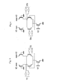
- the figure 3 is an example of an electronic circuit that can act as a buffer circuit 50 made with a differential architecture (the data received and all the signals being transmitted on two complementary channels in phase opposition).
- the figure 4 is an example of an electronic circuit, with a differential architecture, which can act as a delay element of the delay circuit 54, the latter comprising a plurality of such elements in series whose number is adapted to determine the width of the pulses to be formed.
- the figure 5 is a example of an electronic circuit with a differential architecture that can be used to realize the exclusive OR gate 53.
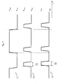
- the figure 7 is a timing diagram illustrating an example of a received signal (curve C1), the corresponding form of the voltage pulses generated by the phase pulse generator 30 (curve C2), and the corresponding form of the current pulses generated by the generator of synchronization pulses 20 (curve C3).
- the phase comparator 26 has an output 33 on which it delivers an amplitude signal proportional to the phase shift between its two inputs 27, 28, that is to say the difference in phase between the received signal (the pulses delivered by the phase pulse generator 30 being in phase with the edges of the received signal) and the reception clock signal supplied by the oscillator 19.
- the signal delivered on the output 33 of the phase comparator 26 is at a rest value which is adapted to have no effect on the oscillator 19.
- This idle value can be a zero value or another value, depending on the characteristics of the the control input 24 of the oscillator 19.
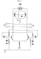
- the figure 6 is an example of an electronic circuit with a differential architecture that can be used to realize the phase comparator 26 in the form of an exclusive OR gate having a single output terminal delivering a current signal and forming via an output impedance 38, the output 33 in voltage of the phase comparator 26.
- this circuit is a multiplier.
- the amplitude of the pulses delivered by the phase pulse generator 30 is large enough for this multiplier to operate outside its linear zone, the output current not depending on the amplitude of the input voltages, but only on their phases.
- This multiplier is therefore equivalent to an exclusive OR gate and its gain in phase comparison is maximum, as well as the bandwidth of the loop. phase lock 25, and therefore the capture range of the device according to the invention.
- all or part of the output impedance 38 of the phase comparator 26 can be integrated in the input 34 of the loop filter 35.
- V1 and V2 are bias voltages
- I is a bias current
- the output 33 of the phase comparator 26 is connected to the input 34 of a loop filter 35 generating an average voltage of the signal supplied by the phase comparator 26 and making it possible to filter the high frequency variations of the phase difference between the received signal and the reception clock signal.
- the output 36 of the loop filter 35 is connected to the control input 24 of the oscillator 19, so that the natural frequency fos is slaved to the phase difference between the received signal and the reception clock signal.
- the natural frequency fos of the oscillator is equal to the bit clock frequency fsr of the received signal. If a phase shift occurs, the phase lock loop 25 thus formed makes it possible to modify the value of the natural frequency fos of the oscillator to make up for the phase shift.
- phase control loop 25 Due to the presence of the specific phase pulse generator for supplying the phase comparator 26, the latter can be extremely simple without affecting the capture range of the phase loop 25. No manual external adjustment is necessary in particular as regards the natural frequency fos of the oscillator 19. In addition, whatever the signal received, the phase control loop 25 makes it possible to ensure that the reception clock signal supplied by the oscillator 19 always in phase with the received signal.
- phase shifter circuit (s) 37 placed (s) between the branch node 11 and each of the inputs 17, 18 of the sampling circuit 15. It is indeed important that the sampling circuit 15 conducts a sampling of the signal received in the central zone of the period of each bit of data of the received signal where the value of the corresponding voltage is the most stable and where the noise margin is greatest, and this in order to avoid realizing the sampling at the beginning or the end of the period of each bit where the signal voltage, being set, is subject to phase drift (traditionally referred to as "jitter”) as shown in figure 12 .
- phase drift traditionally referred to as "jitter”
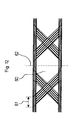
- the figure 12 represents indeed the real pace of a received signal, generally noisy, each bit being in the form of an "eye” taking into account the drift of phase ("jitter") 61.
- the sampling must occur ideally at the center of the eye 60, that is to say at the instant represented by the line 62.
- the difference between the bit clock frequency fsr of the received bits and the oscillation frequency fos of the oscillator 19 being zero in a device according to the invention, and the set of delays that can be introduced by the other components. of the circuit and the set of propagation delays in the various branches of the circuit being controlled and known, it is possible to determine the structural and constant phase differential delay between the data contained in the received signal and the reception clock signal. delivered by the oscillator 19. This differential delay is compensated by the phase-shifter circuit (s) 37.
- a single phase shifter circuit 37 may be provided in the device according to the invention, at any appropriate place.
- the phase shift between the two branches 12, 14 can be obtained by a plurality of phase shifter circuits 37 distributed in several locations of each branch. In the latter case, the accumulation of the phase shifts introduced by each phase shifter circuit 37 is equal to the total phase shift that must be achieved between the two branches 12, 14.
- phase shifter circuit 37 may be provided.
- a phase shifter circuit 37a between the branch node 11 and the input of signal 17 of the sampling circuit 15; a phase shifter circuit 37b between the output 29 of the oscillator 19 and the clock input 18 of the sampling circuit 15; a phase shifter circuit 37c between the branch node 11 and the input 21 of the pulse generator 20 supplying the oscillator 19; a phase shifter circuit 37d between the output 22 of the pulse generator 20 and the input 23 of the oscillator 19; a phase shifter circuit 37e between the branch node 11 and the input 32 of the phase pulse generator 30; a phase shifter circuit 37f between the output 31 of the phase pulse generator 30 and the second input 28 of the phase comparator 26; a phase shifter circuit 37g between the output 29 of the oscillator 19 and the first input 27 of the phase comparator 26.
- Each phase shifter circuit 37 may be formed of a single delay line.
- the embodiment shown figure 4 differs from that of the figure 1 only by the fact that the two pulse generators 20, 30 are replaced by a single pulse generator 40 supplying pulses with two different matching stages 43, 44, connected in parallel with the output 42 of the pulse generator 40.
- the input 41 of the pulse generator 40 is connected to the branch node 11 to receive the received signal, if necessary via a phase shifter circuit 37h.
- the first matching stage 43 provides, as the synchronization pulse generator 20 of the embodiment of the figure 1 current pulses on its output 45 connected to the current input 23 of the oscillator 19, possibly via the phase shifter circuit 37d.
- the second adaptation stage 44 delivers, as the phase pulse generator 30 of the embodiment of the figure 1 , pulses-in particular voltage-on its output 46 connected to the second input 28 of the phase comparator 26, possibly via the phase shifter circuit 37f.
- the pulse generator 40 and the first matching stage 43 together constitute a current synchronization pulse generator circuit.
- the pulse generator 40 and the second matching stage 44 together constitute a phase-pulse generator circuit generating at its output 46 pulses adapted to the
- the device according to the invention comprises two distinct pulse generators, namely a phase pulse generator 40, 44, and a synchronization pulse generator 40, 43.
- the first matching stage 43 is a circuit performing a conversion of the voltage present on the output 42 of the pulse generator 40, in current injected into the oscillator locked by injection.
- the figure 10 illustrates an example of a differential topology electronic circuit of this first adaptation stage 43.
- the second matching stage 44 is a stage matching the amplitude of the voltage present on the output 42 of the pulse generator 40 to the input 28 of the phase comparator.
- the figure 9 illustrates an example of differential topology realization of this second adaptation stage 44.
- a prototype of a device according to the invention according to the electronic circuit represented figure 11 in the form of an ASIC circuit in 0.13 ⁇ m CMOS technology from STMicroelectronics.
- This encapsulated prototype case has been reported on a glass-Teflon circuit board.
- this prototype bare chip has been reported on a substrate alumina.
- These two reports validated the entire operation of this architecture, which has successfully completed complete electrical characterization tests, including thermal tests up to 85 ° C.
- this prototype was subjected to tests under laser beam where errors could only be triggered with a laser at the highest power possible for this type of test, ie 200 pico-joules , equivalent to a LET (Linear Energy Transfer) of approximately 50 MeV / mg / cm2.
- Heavy ion beam tests were also performed, and a LET of 64 MeV / mg / cm2 was required to trigger errors. In all cases, the number of errors observed was particularly small.
- the invention can be the subject of many variants with respect to the embodiments shown in the figures and described above.
- the various components of the device can be produced by other circuit structures, known in themselves, and providing the same functions. .
Landscapes
- Engineering & Computer Science (AREA)
- Computer Networks & Wireless Communication (AREA)
- Signal Processing (AREA)
- Stabilization Of Oscillater, Synchronisation, Frequency Synthesizers (AREA)
- Synchronisation In Digital Transmission Systems (AREA)
Claims (13)
- Vorrichtung zur Extraktion von Takt und digitalen Daten aus einem seriellen Basisband-Signal, Empfangssignal genannt, das digitale Daten repräsentiert und mit einem Taktsignal codiert ist, das eine Taktfrequenz bits fsr aufweist, umfassend:- eine Schaltung (12) zur Taktextraktion, die mit einem Eingang, Empfangseingang (10) genannt, verbunden ist, der das Empfangssignal entgegennimmt, und Folgendes umfasst:-- einen Injektionssynchron-Oszillator (19), der mindestens einen Anschluss, Stromeingang (23) genannt, umfasst, der ein Signal entgegennimmt, das vom Empfangssignal abgeleitet und mit der Taktfrequenz bits fsr getaktet ist, und an mindestens einem Anschluss, Taktausgang (29) genannt, ein Taktsignal, Empfangstaktsignal genannt, abgibt, das mit der Taktfrequenz bits fsr des Empfangssignals synchronisiert und in Phase ist,-- einen Phasenregelkreis (25), umfassend:--- einen ersten Eingang (27), der mit einem Taktausgang (29) des Injektionssynchron-Oszillators verbunden ist,--- einen zweiten Eingang (28), der von einem vom Empfangssignal abgeleiteten Signal gespeist wird,--- und einen Ausgang (36), der ein Analogspannungssignal, Steuersignal genannt, abgibt und mit einem Eingang, Steuereingang (24) genannt, des Oszillators (19) verbunden ist und sich derart verhält, dass der Wert der Eigenfrequenz fos des Oszillators (19) vom Wert des über diesen Steuereingang (24) empfangenen Steuersignals abhängt, wobei der Wert des Steuersignals derart bemessen ist, dass es entweder ohne Wirkung auf den Oszillator (19) ist, wenn nämlich die Phasendifferenz zwischen dem ersten Eingang (27) und dem zweiten Eingang (28) null ist, oder die Eigenfrequenz fos derart modifiziert, dass diese Letztere den Wert der Taktfrequenz bits fsr des Empfangstaktsignals annimmt,-- eine Schaltung, Phasenimpulsgenerator (30) genannt, die ein Impulssignal mit der Frequenz der Flanken des Empfangssignals bei einer Dauer und einer Amplitude der Impulse, die an die Betriebseigenschaften des Phasenregelkreises (25) angepasst sind, erzeugt und diese Impulse über einen einzigen Ausgang (31) abgibt, der nur mit dem zweiten Eingang (28) des Phasenregelkreises (25) verbunden ist,-- eine Synchronisationsimpulsgeneratorschaltung (20, 40, 43), die ein Stromimpulssignal mit der Frequenz der Flanken des Empfangssignals an einem einzigen Ausgang (22, 45) erzeugt, der nur mit dem Stromeingang (23) des Injektionssynchron-Oszillators (19) verbunden ist,- eine Schaltung (15) zum Abtasten des Empfangssignals mit dem Empfangstaktsignal, wobei diese Abtastschaltung (15) einen ersten Eingang, Signaleingang (17) genannt, der mit dem Empfangseingang (10) verbunden ist, und einen zweiten Eingang, Takteingang (18) genannt, der mit mindestens einem Taktausgang (29) des Injektionssynchron-Oszillators verbunden ist, aufweist, wobei diese Abtastschaltung (15) dafür eingerichtet ist, an mindestens einem Anschluss, Datenausgang (16) genannt, vom Empfangssignal übertragene digitale Daten abzugeben,- mindestens eine Phasenschieberschaltung (37), die dafür eingerichtet ist, eine vorgegebene konstante Phasendifferenz zwischen den Signaleingang (17) und den Takteingang (18) der Abtastschaltung (15) einzubringen, wobei die Gesamtphasendifferenz zwischen diesen beiden Eingängen (17, 18), die durch diese Phasenschieberschaltung (37) entsteht, derart bemessen ist, dass ein Phasenabgleich des Signals am Signaleingang (17) und des Signals am Takteingang (18) gewährleistet ist.
- Vorrichtung nach Anspruch 1, dadurch gekennzeichnet, dass der Phasenregelkreis (25) eine Phasenkomparatorschaltung (26) mit einem ersten Eingang (27), der mit dem Taktausgang (29) verbunden ist, einem zweiten Eingang (28), der mit dem Ausgang (31) des Phasenimpulsgenerators (30) verbunden ist, und einem Ausgang (33), der ein Analogsignal abgibt, dessen Amplitude eine Funktion der Phasendifferenz zwischen dem ersten Eingang (27) und dem zweiten Eingang (28) ist, umfasst, und dadurch, dass der Phasenimpulsgenerator (30) dafür eingerichtet ist, ein Impulssignal mit einer Dauer und einer Amplitude der Impulse zu erzeugen, die an die Betriebseigenschaften dieses Phasenkomparators (26) angepasst sind.
- Vorrichtung nach Anspruch 2, dadurch gekennzeichnet, dass der Ausgang (33) des Phasenkomparators (26) mit dem Eingang (34) eines Schleifenfilters (35) verbunden ist, wobei dieses Schleifenfilter (35) einen Ausgang (36) umfasst, der das Steuersignal abgibt.
- Vorrichtung nach einem der Ansprüche 1 bis 3, dadurch gekennzeichnet, dass der Phasenimpulsgenerator (30) dafür eingerichtet ist, ein Spannungsimpulssignal abzugeben.
- Vorrichtung nach einem der Ansprüche 1 bis 4, dadurch gekennzeichnet, dass der Phasenimpulsgenerator (30) dafür eingerichtet ist, Impulse abzugeben, die eine Breite aufweisen, die gleich der Hälfte der Nenndauer eines Bits des Empfangssignals ist.
- Vorrichtung nach einem der Ansprüche 1 bis 5, dadurch gekennzeichnet, dass der Phasenkomparator (26) von einem Exklusiv-ODER-Gatter gebildet wird.
- Vorrichtung nach einem der Ansprüche 1 bis 6, dadurch gekennzeichnet, dass der Injektionssynchron-Oszillator (19) von dem Typ ist, der von einem LC-Resonanzkreis gebildet wird.
- Vorrichtung nach Anspruch 7, dadurch gekennzeichnet, dass der Injektionssynchron-Oszillator (19) zwei Zweige mit jeweils einem Feldeffekttransistor mit negativem Widerstand umfasst, wobei die beiden Transistoren gemäß einer differentiellen Topologie gekoppelt sind.
- Vorrichtung nach einem der Ansprüche 1 bis 8, dadurch gekennzeichnet, dass sie frei von externen Regelungsmitteln ist.
- Vorrichtung nach einem der Ansprüche 1 bis 9, dadurch gekennzeichnet, dass die Abtastschaltung (15) von einer Kippschaltung D gebildet wird.
- Vorrichtung nach einem der Ansprüche 1 bis 10, dadurch gekennzeichnet, dass sie gemäß einer differentiellen Architektur verwirklicht ist.
- Vorrichtung nach einem der Ansprüche 1 bis 11, dadurch gekennzeichnet, dass sie in Form mindestens einer integrierten Schaltung verwirklicht ist, die mindestens einen Injektionssynchron-Oszillator (19) enthält.
- Vorrichtung nach einem der Ansprüche 1 bis 12, dadurch gekennzeichnet, dass sie dafür eingerichtet ist, mit einer Taktfrequenz bits fsr arbeiten zu können, die höher als 500 MHz ist.
Applications Claiming Priority (2)
| Application Number | Priority Date | Filing Date | Title |
|---|---|---|---|
| FR0702555A FR2914808B1 (fr) | 2007-04-06 | 2007-04-06 | Dispositif d'extraction d'horloge et de donnees numeriques sans reglage externe |
| PCT/FR2008/000478 WO2008139063A2 (fr) | 2007-04-06 | 2008-04-04 | Dispositif d'extraction d'horloge et de donnees numeriques sans reglage externe |
Publications (2)
| Publication Number | Publication Date |
|---|---|
| EP2143231A2 EP2143231A2 (de) | 2010-01-13 |
| EP2143231B1 true EP2143231B1 (de) | 2016-08-31 |
Family
ID=38566953
Family Applications (1)
| Application Number | Title | Priority Date | Filing Date |
|---|---|---|---|
| EP08787917.7A Active EP2143231B1 (de) | 2007-04-06 | 2008-04-04 | Vorrichtung zur rückgewinnung des taktes und digitaler daten ohne extenre regelung |
Country Status (3)
| Country | Link |
|---|---|
| EP (1) | EP2143231B1 (de) |
| FR (1) | FR2914808B1 (de) |
| WO (1) | WO2008139063A2 (de) |
Families Citing this family (2)
| Publication number | Priority date | Publication date | Assignee | Title |
|---|---|---|---|---|
| WO2015038867A1 (en) * | 2013-09-16 | 2015-03-19 | Rambus Inc. | Source-synchronous receiver using edged-detection clock recovery |
| CN114938258B (zh) * | 2022-07-25 | 2022-10-14 | 星河动力(北京)空间科技有限公司 | 火箭控制时钟同步装置、飞行控制器和箭上控制计算机 |
Citations (1)
| Publication number | Priority date | Publication date | Assignee | Title |
|---|---|---|---|---|
| US3010073A (en) * | 1959-11-09 | 1961-11-21 | Ibm | Periodic signal generator |
Family Cites Families (6)
| Publication number | Priority date | Publication date | Assignee | Title |
|---|---|---|---|---|
| US3609408A (en) * | 1969-09-30 | 1971-09-28 | Rca Corp | Clock pulse generator |
| SE506470C2 (sv) * | 1996-04-29 | 1997-12-22 | Ericsson Telefon Ab L M | Förfarande och anordning för klockåtervinning ur en datasignal |
| US6317008B1 (en) * | 1998-01-26 | 2001-11-13 | Agere Systems Guardian Corp. | Clock recovery using an injection tuned resonant circuit |
| JP3931477B2 (ja) * | 1998-12-03 | 2007-06-13 | 三菱電機株式会社 | クロック再生/識別装置 |
| CN1167199C (zh) * | 2000-06-08 | 2004-09-15 | 华为技术有限公司 | 注入型同步窄带再生锁相环 |
| FR2838265B1 (fr) * | 2002-04-04 | 2004-09-17 | Centre Nat Etd Spatiales | Procede et dispositif de transmission de donnees numeriques en serie |
-
2007
- 2007-04-06 FR FR0702555A patent/FR2914808B1/fr active Active
-
2008
- 2008-04-04 WO PCT/FR2008/000478 patent/WO2008139063A2/fr not_active Ceased
- 2008-04-04 EP EP08787917.7A patent/EP2143231B1/de active Active
Patent Citations (1)
| Publication number | Priority date | Publication date | Assignee | Title |
|---|---|---|---|---|
| US3010073A (en) * | 1959-11-09 | 1961-11-21 | Ibm | Periodic signal generator |
Also Published As
| Publication number | Publication date |
|---|---|
| FR2914808B1 (fr) | 2009-06-05 |
| FR2914808A1 (fr) | 2008-10-10 |
| WO2008139063A2 (fr) | 2008-11-20 |
| WO2008139063A3 (fr) | 2008-12-31 |
| EP2143231A2 (de) | 2010-01-13 |
Similar Documents
| Publication | Publication Date | Title |
|---|---|---|
| EP2137873B1 (de) | Vorrichtung zur rückgewinnung des taktsignales zur digitalen regelung der phase ohne externe regelung | |
| EP2494693B1 (de) | Vorrichtung zur erzeugung von taktsignalen für den asymmetrischen vergleich von phasenfehlern | |
| EP1863179B1 (de) | Niveauverschiebungsschaltkreis | |
| EP1956714A1 (de) | Verfahren zum Hinzufügen eines zufallsbedingten Rauschens in einen Zeit-Digital-Wandlungsschaltkreis und Schaltkreise zur Umsetzung des Verfahrens | |
| EP2786492B1 (de) | Frequenzsynthesevorrichtung und -verfahren | |
| EP0358144B1 (de) | Mit einer hohen Frequenz modulierte Halbleiterlaserquelle | |
| EP1049285A1 (de) | Frequenzregelkreis | |
| FR3133458A1 (fr) | Circuit de génération de séquence temporelle | |
| EP0881772A1 (de) | Frequenzteilungsvorrichtung, bestehend aus einem Vorzähler gefolgt von einem programmierbaren Zähler und Anwendung in einem Frequenzsynthetisierer | |
| EP1351428B1 (de) | Verfahren und Vorrichtung zur Taktrückgewinnung | |
| EP2143231A2 (de) | Digitales daten- und taktextraktionsgerät ohne notwendigkeit externer steuerung | |
| EP1606880B1 (de) | Frequenzteiler mit veränderlicher teilungsrate | |
| EP0696116B1 (de) | Verfahren zum Abtasten eines seriellen digitalen Signals | |
| EP0302562A1 (de) | Frequenz-Synthetisierer mit einer Abstimm-Anzeigeeinrichtung | |
| EP3048730B1 (de) | Vorrichtung zur erzeugung einer rückkopplungsschleifenfrequenz | |
| FR2986679A1 (fr) | Generateur de nombres aleatoires vrais | |
| EP1710916B1 (de) | Phasenregelschleife | |
| EP2127112A1 (de) | Funkübertragungseinrichtung | |
| EP3764546B1 (de) | Vorrichtung zur frequenzsynthese mit rückkopplungsschleife | |
| FR2816075A1 (fr) | Generateur ameliore pour la production de signaux d'horloge | |
| Abbas et al. | Fast-Locking Burst-Mode Clock and Data Recovery for Parallel VCSEL-Based Optical Link Receivers | |
| FR3025901A1 (fr) | Dispositif de generation d'un signal d'horloge par multiplication de frequence | |
| EP4648283A1 (de) | Vorrichtung zur erzeugung einer zeitsequenz | |
| FR2905040A1 (fr) | Procede d'elaboration d'un mot numerique representatif d'un rapport non-entier entre les periodes respectives de deux signaux, et dispositif correspondant | |
| EP4184791A1 (de) | Wellensignalgenerator |
Legal Events
| Date | Code | Title | Description |
|---|---|---|---|
| PUAI | Public reference made under article 153(3) epc to a published international application that has entered the european phase |
Free format text: ORIGINAL CODE: 0009012 |
|
| 17P | Request for examination filed |
Effective date: 20091104 |
|
| AK | Designated contracting states |
Kind code of ref document: A2 Designated state(s): AT BE BG CH CY CZ DE DK EE ES FI FR GB GR HR HU IE IS IT LI LT LU LV MC MT NL NO PL PT RO SE SI SK TR |
|
| DAX | Request for extension of the european patent (deleted) | ||
| 17Q | First examination report despatched |
Effective date: 20140205 |
|
| GRAP | Despatch of communication of intention to grant a patent |
Free format text: ORIGINAL CODE: EPIDOSNIGR1 |
|
| INTG | Intention to grant announced |
Effective date: 20160413 |
|
| GRAS | Grant fee paid |
Free format text: ORIGINAL CODE: EPIDOSNIGR3 |
|
| GRAA | (expected) grant |
Free format text: ORIGINAL CODE: 0009210 |
|
| AK | Designated contracting states |
Kind code of ref document: B1 Designated state(s): AT BE BG CH CY CZ DE DK EE ES FI FR GB GR HR HU IE IS IT LI LT LU LV MC MT NL NO PL PT RO SE SI SK TR |
|
| REG | Reference to a national code |
Ref country code: CH Ref legal event code: EP Ref country code: GB Ref legal event code: FG4D Free format text: NOT ENGLISH |
|
| REG | Reference to a national code |
Ref country code: IE Ref legal event code: FG4D Free format text: LANGUAGE OF EP DOCUMENT: FRENCH |
|
| REG | Reference to a national code |
Ref country code: DE Ref legal event code: R096 Ref document number: 602008046021 Country of ref document: DE |
|
| REG | Reference to a national code |
Ref country code: AT Ref legal event code: REF Ref document number: 825793 Country of ref document: AT Kind code of ref document: T Effective date: 20161015 |
|
| REG | Reference to a national code |
Ref country code: LT Ref legal event code: MG4D |
|
| REG | Reference to a national code |
Ref country code: NL Ref legal event code: MP Effective date: 20160831 |
|
| REG | Reference to a national code |
Ref country code: AT Ref legal event code: MK05 Ref document number: 825793 Country of ref document: AT Kind code of ref document: T Effective date: 20160831 |
|
| PG25 | Lapsed in a contracting state [announced via postgrant information from national office to epo] |
Ref country code: NO Free format text: LAPSE BECAUSE OF FAILURE TO SUBMIT A TRANSLATION OF THE DESCRIPTION OR TO PAY THE FEE WITHIN THE PRESCRIBED TIME-LIMIT Effective date: 20161130 Ref country code: FI Free format text: LAPSE BECAUSE OF FAILURE TO SUBMIT A TRANSLATION OF THE DESCRIPTION OR TO PAY THE FEE WITHIN THE PRESCRIBED TIME-LIMIT Effective date: 20160831 Ref country code: HR Free format text: LAPSE BECAUSE OF FAILURE TO SUBMIT A TRANSLATION OF THE DESCRIPTION OR TO PAY THE FEE WITHIN THE PRESCRIBED TIME-LIMIT Effective date: 20160831 Ref country code: LT Free format text: LAPSE BECAUSE OF FAILURE TO SUBMIT A TRANSLATION OF THE DESCRIPTION OR TO PAY THE FEE WITHIN THE PRESCRIBED TIME-LIMIT Effective date: 20160831 |
|
| PG25 | Lapsed in a contracting state [announced via postgrant information from national office to epo] |
Ref country code: SE Free format text: LAPSE BECAUSE OF FAILURE TO SUBMIT A TRANSLATION OF THE DESCRIPTION OR TO PAY THE FEE WITHIN THE PRESCRIBED TIME-LIMIT Effective date: 20160831 Ref country code: GR Free format text: LAPSE BECAUSE OF FAILURE TO SUBMIT A TRANSLATION OF THE DESCRIPTION OR TO PAY THE FEE WITHIN THE PRESCRIBED TIME-LIMIT Effective date: 20161201 Ref country code: AT Free format text: LAPSE BECAUSE OF FAILURE TO SUBMIT A TRANSLATION OF THE DESCRIPTION OR TO PAY THE FEE WITHIN THE PRESCRIBED TIME-LIMIT Effective date: 20160831 Ref country code: LV Free format text: LAPSE BECAUSE OF FAILURE TO SUBMIT A TRANSLATION OF THE DESCRIPTION OR TO PAY THE FEE WITHIN THE PRESCRIBED TIME-LIMIT Effective date: 20160831 Ref country code: ES Free format text: LAPSE BECAUSE OF FAILURE TO SUBMIT A TRANSLATION OF THE DESCRIPTION OR TO PAY THE FEE WITHIN THE PRESCRIBED TIME-LIMIT Effective date: 20160831 Ref country code: NL Free format text: LAPSE BECAUSE OF FAILURE TO SUBMIT A TRANSLATION OF THE DESCRIPTION OR TO PAY THE FEE WITHIN THE PRESCRIBED TIME-LIMIT Effective date: 20160831 |
|
| PG25 | Lapsed in a contracting state [announced via postgrant information from national office to epo] |
Ref country code: EE Free format text: LAPSE BECAUSE OF FAILURE TO SUBMIT A TRANSLATION OF THE DESCRIPTION OR TO PAY THE FEE WITHIN THE PRESCRIBED TIME-LIMIT Effective date: 20160831 Ref country code: RO Free format text: LAPSE BECAUSE OF FAILURE TO SUBMIT A TRANSLATION OF THE DESCRIPTION OR TO PAY THE FEE WITHIN THE PRESCRIBED TIME-LIMIT Effective date: 20160831 |
|
| REG | Reference to a national code |
Ref country code: FR Ref legal event code: PLFP Year of fee payment: 10 |
|
| PG25 | Lapsed in a contracting state [announced via postgrant information from national office to epo] |
Ref country code: PL Free format text: LAPSE BECAUSE OF FAILURE TO SUBMIT A TRANSLATION OF THE DESCRIPTION OR TO PAY THE FEE WITHIN THE PRESCRIBED TIME-LIMIT Effective date: 20160831 Ref country code: PT Free format text: LAPSE BECAUSE OF FAILURE TO SUBMIT A TRANSLATION OF THE DESCRIPTION OR TO PAY THE FEE WITHIN THE PRESCRIBED TIME-LIMIT Effective date: 20170102 Ref country code: SK Free format text: LAPSE BECAUSE OF FAILURE TO SUBMIT A TRANSLATION OF THE DESCRIPTION OR TO PAY THE FEE WITHIN THE PRESCRIBED TIME-LIMIT Effective date: 20160831 Ref country code: CZ Free format text: LAPSE BECAUSE OF FAILURE TO SUBMIT A TRANSLATION OF THE DESCRIPTION OR TO PAY THE FEE WITHIN THE PRESCRIBED TIME-LIMIT Effective date: 20160831 Ref country code: DK Free format text: LAPSE BECAUSE OF FAILURE TO SUBMIT A TRANSLATION OF THE DESCRIPTION OR TO PAY THE FEE WITHIN THE PRESCRIBED TIME-LIMIT Effective date: 20160831 Ref country code: BG Free format text: LAPSE BECAUSE OF FAILURE TO SUBMIT A TRANSLATION OF THE DESCRIPTION OR TO PAY THE FEE WITHIN THE PRESCRIBED TIME-LIMIT Effective date: 20161130 |
|
| REG | Reference to a national code |
Ref country code: DE Ref legal event code: R097 Ref document number: 602008046021 Country of ref document: DE |
|
| PG25 | Lapsed in a contracting state [announced via postgrant information from national office to epo] |
Ref country code: IT Free format text: LAPSE BECAUSE OF FAILURE TO SUBMIT A TRANSLATION OF THE DESCRIPTION OR TO PAY THE FEE WITHIN THE PRESCRIBED TIME-LIMIT Effective date: 20160831 |
|
| PLBE | No opposition filed within time limit |
Free format text: ORIGINAL CODE: 0009261 |
|
| STAA | Information on the status of an ep patent application or granted ep patent |
Free format text: STATUS: NO OPPOSITION FILED WITHIN TIME LIMIT |
|
| 26N | No opposition filed |
Effective date: 20170601 |
|
| PG25 | Lapsed in a contracting state [announced via postgrant information from national office to epo] |
Ref country code: SI Free format text: LAPSE BECAUSE OF FAILURE TO SUBMIT A TRANSLATION OF THE DESCRIPTION OR TO PAY THE FEE WITHIN THE PRESCRIBED TIME-LIMIT Effective date: 20160831 |
|
| REG | Reference to a national code |
Ref country code: CH Ref legal event code: PL |
|
| REG | Reference to a national code |
Ref country code: IE Ref legal event code: MM4A |
|
| PG25 | Lapsed in a contracting state [announced via postgrant information from national office to epo] |
Ref country code: MC Free format text: LAPSE BECAUSE OF FAILURE TO SUBMIT A TRANSLATION OF THE DESCRIPTION OR TO PAY THE FEE WITHIN THE PRESCRIBED TIME-LIMIT Effective date: 20160831 |
|
| PG25 | Lapsed in a contracting state [announced via postgrant information from national office to epo] |
Ref country code: CH Free format text: LAPSE BECAUSE OF NON-PAYMENT OF DUE FEES Effective date: 20170430 Ref country code: LU Free format text: LAPSE BECAUSE OF NON-PAYMENT OF DUE FEES Effective date: 20170404 Ref country code: LI Free format text: LAPSE BECAUSE OF NON-PAYMENT OF DUE FEES Effective date: 20170430 |
|
| REG | Reference to a national code |
Ref country code: BE Ref legal event code: MM Effective date: 20170430 |
|
| REG | Reference to a national code |
Ref country code: FR Ref legal event code: PLFP Year of fee payment: 11 |
|
| PG25 | Lapsed in a contracting state [announced via postgrant information from national office to epo] |
Ref country code: IE Free format text: LAPSE BECAUSE OF NON-PAYMENT OF DUE FEES Effective date: 20170404 |
|
| PG25 | Lapsed in a contracting state [announced via postgrant information from national office to epo] |
Ref country code: BE Free format text: LAPSE BECAUSE OF NON-PAYMENT OF DUE FEES Effective date: 20170430 |
|
| PG25 | Lapsed in a contracting state [announced via postgrant information from national office to epo] |
Ref country code: MT Free format text: LAPSE BECAUSE OF FAILURE TO SUBMIT A TRANSLATION OF THE DESCRIPTION OR TO PAY THE FEE WITHIN THE PRESCRIBED TIME-LIMIT Effective date: 20160831 |
|
| PG25 | Lapsed in a contracting state [announced via postgrant information from national office to epo] |
Ref country code: HU Free format text: LAPSE BECAUSE OF FAILURE TO SUBMIT A TRANSLATION OF THE DESCRIPTION OR TO PAY THE FEE WITHIN THE PRESCRIBED TIME-LIMIT; INVALID AB INITIO Effective date: 20080404 |
|
| PG25 | Lapsed in a contracting state [announced via postgrant information from national office to epo] |
Ref country code: CY Free format text: LAPSE BECAUSE OF NON-PAYMENT OF DUE FEES Effective date: 20160831 |
|
| PG25 | Lapsed in a contracting state [announced via postgrant information from national office to epo] |
Ref country code: TR Free format text: LAPSE BECAUSE OF FAILURE TO SUBMIT A TRANSLATION OF THE DESCRIPTION OR TO PAY THE FEE WITHIN THE PRESCRIBED TIME-LIMIT Effective date: 20160831 |
|
| PG25 | Lapsed in a contracting state [announced via postgrant information from national office to epo] |
Ref country code: IS Free format text: LAPSE BECAUSE OF FAILURE TO SUBMIT A TRANSLATION OF THE DESCRIPTION OR TO PAY THE FEE WITHIN THE PRESCRIBED TIME-LIMIT Effective date: 20161231 |
|
| PGFP | Annual fee paid to national office [announced via postgrant information from national office to epo] |
Ref country code: GB Payment date: 20260316 Year of fee payment: 19 |
|
| PGFP | Annual fee paid to national office [announced via postgrant information from national office to epo] |
Ref country code: FR Payment date: 20260316 Year of fee payment: 19 |
|
| PGFP | Annual fee paid to national office [announced via postgrant information from national office to epo] |
Ref country code: DE Payment date: 20260316 Year of fee payment: 19 |