EP2144111A1 - Aktivmatrixsubstrat, flüssigkristalltafel, flüssigkristallanzeigeeheit, flüssigkristallanzeige und fernsehempfänger - Google Patents
Aktivmatrixsubstrat, flüssigkristalltafel, flüssigkristallanzeigeeheit, flüssigkristallanzeige und fernsehempfänger Download PDFInfo
- Publication number
- EP2144111A1 EP2144111A1 EP08710850A EP08710850A EP2144111A1 EP 2144111 A1 EP2144111 A1 EP 2144111A1 EP 08710850 A EP08710850 A EP 08710850A EP 08710850 A EP08710850 A EP 08710850A EP 2144111 A1 EP2144111 A1 EP 2144111A1
- Authority
- EP
- European Patent Office
- Prior art keywords
- pixel
- liquid crystal
- storage capacitor
- signal line
- data signal
- Prior art date
- Legal status (The legal status is an assumption and is not a legal conclusion. Google has not performed a legal analysis and makes no representation as to the accuracy of the status listed.)
- Withdrawn
Links
Images














Classifications
-
- G—PHYSICS
- G02—OPTICS
- G02F—OPTICAL DEVICES OR ARRANGEMENTS FOR THE CONTROL OF LIGHT BY MODIFICATION OF THE OPTICAL PROPERTIES OF THE MEDIA OF THE ELEMENTS INVOLVED THEREIN; NON-LINEAR OPTICS; FREQUENCY-CHANGING OF LIGHT; OPTICAL LOGIC ELEMENTS; OPTICAL ANALOGUE/DIGITAL CONVERTERS
- G02F1/00—Devices or arrangements for the control of the intensity, colour, phase, polarisation or direction of light arriving from an independent light source, e.g. switching, gating or modulating; Non-linear optics
- G02F1/01—Devices or arrangements for the control of the intensity, colour, phase, polarisation or direction of light arriving from an independent light source, e.g. switching, gating or modulating; Non-linear optics for the control of the intensity, phase, polarisation or colour
- G02F1/13—Devices or arrangements for the control of the intensity, colour, phase, polarisation or direction of light arriving from an independent light source, e.g. switching, gating or modulating; Non-linear optics for the control of the intensity, phase, polarisation or colour based on liquid crystals, e.g. single liquid crystal display cells
- G02F1/133—Constructional arrangements; Operation of liquid crystal cells; Circuit arrangements
- G02F1/136—Liquid crystal cells structurally associated with a semi-conducting layer or substrate, e.g. cells forming part of an integrated circuit
- G02F1/1362—Active matrix addressed cells
- G02F1/13624—Active matrix addressed cells having more than one switching element per pixel
-
- G—PHYSICS
- G02—OPTICS
- G02F—OPTICAL DEVICES OR ARRANGEMENTS FOR THE CONTROL OF LIGHT BY MODIFICATION OF THE OPTICAL PROPERTIES OF THE MEDIA OF THE ELEMENTS INVOLVED THEREIN; NON-LINEAR OPTICS; FREQUENCY-CHANGING OF LIGHT; OPTICAL LOGIC ELEMENTS; OPTICAL ANALOGUE/DIGITAL CONVERTERS
- G02F1/00—Devices or arrangements for the control of the intensity, colour, phase, polarisation or direction of light arriving from an independent light source, e.g. switching, gating or modulating; Non-linear optics
- G02F1/01—Devices or arrangements for the control of the intensity, colour, phase, polarisation or direction of light arriving from an independent light source, e.g. switching, gating or modulating; Non-linear optics for the control of the intensity, phase, polarisation or colour
- G02F1/13—Devices or arrangements for the control of the intensity, colour, phase, polarisation or direction of light arriving from an independent light source, e.g. switching, gating or modulating; Non-linear optics for the control of the intensity, phase, polarisation or colour based on liquid crystals, e.g. single liquid crystal display cells
- G02F1/133—Constructional arrangements; Operation of liquid crystal cells; Circuit arrangements
- G02F1/1333—Constructional arrangements; Manufacturing methods
- G02F1/1337—Surface-induced orientation of the liquid crystal molecules, e.g. by alignment layers
- G02F1/133707—Structures for producing distorted electric fields, e.g. bumps, protrusions, recesses, slits in pixel electrodes
-
- G—PHYSICS
- G09—EDUCATION; CRYPTOGRAPHY; DISPLAY; ADVERTISING; SEALS
- G09G—ARRANGEMENTS OR CIRCUITS FOR CONTROL OF INDICATING DEVICES USING STATIC MEANS TO PRESENT VARIABLE INFORMATION
- G09G3/00—Control arrangements or circuits, of interest only in connection with visual indicators other than cathode-ray tubes
- G09G3/20—Control arrangements or circuits, of interest only in connection with visual indicators other than cathode-ray tubes for presentation of an assembly of a number of characters, e.g. a page, by composing the assembly by combination of individual elements arranged in a matrix no fixed position being assigned to or needed to be assigned to the individual characters or partial characters
- G09G3/34—Control arrangements or circuits, of interest only in connection with visual indicators other than cathode-ray tubes for presentation of an assembly of a number of characters, e.g. a page, by composing the assembly by combination of individual elements arranged in a matrix no fixed position being assigned to or needed to be assigned to the individual characters or partial characters by control of light from an independent source
- G09G3/36—Control arrangements or circuits, of interest only in connection with visual indicators other than cathode-ray tubes for presentation of an assembly of a number of characters, e.g. a page, by composing the assembly by combination of individual elements arranged in a matrix no fixed position being assigned to or needed to be assigned to the individual characters or partial characters by control of light from an independent source using liquid crystals
- G09G3/3611—Control of matrices with row and column drivers
- G09G3/3648—Control of matrices with row and column drivers using an active matrix
- G09G3/3655—Details of drivers for counter electrodes, e.g. common electrodes for pixel capacitors or supplementary storage capacitors
-
- G—PHYSICS
- G02—OPTICS
- G02F—OPTICAL DEVICES OR ARRANGEMENTS FOR THE CONTROL OF LIGHT BY MODIFICATION OF THE OPTICAL PROPERTIES OF THE MEDIA OF THE ELEMENTS INVOLVED THEREIN; NON-LINEAR OPTICS; FREQUENCY-CHANGING OF LIGHT; OPTICAL LOGIC ELEMENTS; OPTICAL ANALOGUE/DIGITAL CONVERTERS
- G02F1/00—Devices or arrangements for the control of the intensity, colour, phase, polarisation or direction of light arriving from an independent light source, e.g. switching, gating or modulating; Non-linear optics
- G02F1/01—Devices or arrangements for the control of the intensity, colour, phase, polarisation or direction of light arriving from an independent light source, e.g. switching, gating or modulating; Non-linear optics for the control of the intensity, phase, polarisation or colour
- G02F1/13—Devices or arrangements for the control of the intensity, colour, phase, polarisation or direction of light arriving from an independent light source, e.g. switching, gating or modulating; Non-linear optics for the control of the intensity, phase, polarisation or colour based on liquid crystals, e.g. single liquid crystal display cells
- G02F1/133—Constructional arrangements; Operation of liquid crystal cells; Circuit arrangements
- G02F1/1333—Constructional arrangements; Manufacturing methods
- G02F1/1337—Surface-induced orientation of the liquid crystal molecules, e.g. by alignment layers
- G02F1/133776—Surface-induced orientation of the liquid crystal molecules, e.g. by alignment layers having structures locally influencing the alignment, e.g. unevenness
-
- G—PHYSICS
- G02—OPTICS
- G02F—OPTICAL DEVICES OR ARRANGEMENTS FOR THE CONTROL OF LIGHT BY MODIFICATION OF THE OPTICAL PROPERTIES OF THE MEDIA OF THE ELEMENTS INVOLVED THEREIN; NON-LINEAR OPTICS; FREQUENCY-CHANGING OF LIGHT; OPTICAL LOGIC ELEMENTS; OPTICAL ANALOGUE/DIGITAL CONVERTERS
- G02F1/00—Devices or arrangements for the control of the intensity, colour, phase, polarisation or direction of light arriving from an independent light source, e.g. switching, gating or modulating; Non-linear optics
- G02F1/01—Devices or arrangements for the control of the intensity, colour, phase, polarisation or direction of light arriving from an independent light source, e.g. switching, gating or modulating; Non-linear optics for the control of the intensity, phase, polarisation or colour
- G02F1/13—Devices or arrangements for the control of the intensity, colour, phase, polarisation or direction of light arriving from an independent light source, e.g. switching, gating or modulating; Non-linear optics for the control of the intensity, phase, polarisation or colour based on liquid crystals, e.g. single liquid crystal display cells
- G02F1/133—Constructional arrangements; Operation of liquid crystal cells; Circuit arrangements
- G02F1/1333—Constructional arrangements; Manufacturing methods
- G02F1/1343—Electrodes
- G02F1/134309—Electrodes characterised by their geometrical arrangement
- G02F1/134345—Subdivided pixels, e.g. for grey scale or redundancy
-
- G—PHYSICS
- G02—OPTICS
- G02F—OPTICAL DEVICES OR ARRANGEMENTS FOR THE CONTROL OF LIGHT BY MODIFICATION OF THE OPTICAL PROPERTIES OF THE MEDIA OF THE ELEMENTS INVOLVED THEREIN; NON-LINEAR OPTICS; FREQUENCY-CHANGING OF LIGHT; OPTICAL LOGIC ELEMENTS; OPTICAL ANALOGUE/DIGITAL CONVERTERS
- G02F1/00—Devices or arrangements for the control of the intensity, colour, phase, polarisation or direction of light arriving from an independent light source, e.g. switching, gating or modulating; Non-linear optics
- G02F1/01—Devices or arrangements for the control of the intensity, colour, phase, polarisation or direction of light arriving from an independent light source, e.g. switching, gating or modulating; Non-linear optics for the control of the intensity, phase, polarisation or colour
- G02F1/13—Devices or arrangements for the control of the intensity, colour, phase, polarisation or direction of light arriving from an independent light source, e.g. switching, gating or modulating; Non-linear optics for the control of the intensity, phase, polarisation or colour based on liquid crystals, e.g. single liquid crystal display cells
- G02F1/133—Constructional arrangements; Operation of liquid crystal cells; Circuit arrangements
- G02F1/136—Liquid crystal cells structurally associated with a semi-conducting layer or substrate, e.g. cells forming part of an integrated circuit
- G02F1/1362—Active matrix addressed cells
- G02F1/136213—Storage capacitors associated with the pixel electrode
-
- G—PHYSICS
- G02—OPTICS
- G02F—OPTICAL DEVICES OR ARRANGEMENTS FOR THE CONTROL OF LIGHT BY MODIFICATION OF THE OPTICAL PROPERTIES OF THE MEDIA OF THE ELEMENTS INVOLVED THEREIN; NON-LINEAR OPTICS; FREQUENCY-CHANGING OF LIGHT; OPTICAL LOGIC ELEMENTS; OPTICAL ANALOGUE/DIGITAL CONVERTERS
- G02F1/00—Devices or arrangements for the control of the intensity, colour, phase, polarisation or direction of light arriving from an independent light source, e.g. switching, gating or modulating; Non-linear optics
- G02F1/01—Devices or arrangements for the control of the intensity, colour, phase, polarisation or direction of light arriving from an independent light source, e.g. switching, gating or modulating; Non-linear optics for the control of the intensity, phase, polarisation or colour
- G02F1/13—Devices or arrangements for the control of the intensity, colour, phase, polarisation or direction of light arriving from an independent light source, e.g. switching, gating or modulating; Non-linear optics for the control of the intensity, phase, polarisation or colour based on liquid crystals, e.g. single liquid crystal display cells
- G02F1/133—Constructional arrangements; Operation of liquid crystal cells; Circuit arrangements
- G02F1/136—Liquid crystal cells structurally associated with a semi-conducting layer or substrate, e.g. cells forming part of an integrated circuit
- G02F1/1362—Active matrix addressed cells
- G02F1/136286—Wiring, e.g. gate line, drain line
-
- G—PHYSICS
- G09—EDUCATION; CRYPTOGRAPHY; DISPLAY; ADVERTISING; SEALS
- G09G—ARRANGEMENTS OR CIRCUITS FOR CONTROL OF INDICATING DEVICES USING STATIC MEANS TO PRESENT VARIABLE INFORMATION
- G09G2300/00—Aspects of the constitution of display devices
- G09G2300/04—Structural and physical details of display devices
- G09G2300/0421—Structural details of the set of electrodes
- G09G2300/0426—Layout of electrodes and connections
-
- G—PHYSICS
- G09—EDUCATION; CRYPTOGRAPHY; DISPLAY; ADVERTISING; SEALS
- G09G—ARRANGEMENTS OR CIRCUITS FOR CONTROL OF INDICATING DEVICES USING STATIC MEANS TO PRESENT VARIABLE INFORMATION
- G09G2300/00—Aspects of the constitution of display devices
- G09G2300/04—Structural and physical details of display devices
- G09G2300/0439—Pixel structures
- G09G2300/0443—Pixel structures with several sub-pixels for the same colour in a pixel, not specifically used to display gradations
-
- G—PHYSICS
- G09—EDUCATION; CRYPTOGRAPHY; DISPLAY; ADVERTISING; SEALS
- G09G—ARRANGEMENTS OR CIRCUITS FOR CONTROL OF INDICATING DEVICES USING STATIC MEANS TO PRESENT VARIABLE INFORMATION
- G09G2320/00—Control of display operating conditions
- G09G2320/02—Improving the quality of display appearance
- G09G2320/0233—Improving the luminance or brightness uniformity across the screen
-
- G—PHYSICS
- G09—EDUCATION; CRYPTOGRAPHY; DISPLAY; ADVERTISING; SEALS
- G09G—ARRANGEMENTS OR CIRCUITS FOR CONTROL OF INDICATING DEVICES USING STATIC MEANS TO PRESENT VARIABLE INFORMATION
- G09G2320/00—Control of display operating conditions
- G09G2320/02—Improving the quality of display appearance
- G09G2320/028—Improving the quality of display appearance by changing the viewing angle properties, e.g. widening the viewing angle, adapting the viewing angle to the view direction
-
- G—PHYSICS
- G09—EDUCATION; CRYPTOGRAPHY; DISPLAY; ADVERTISING; SEALS
- G09G—ARRANGEMENTS OR CIRCUITS FOR CONTROL OF INDICATING DEVICES USING STATIC MEANS TO PRESENT VARIABLE INFORMATION
- G09G3/00—Control arrangements or circuits, of interest only in connection with visual indicators other than cathode-ray tubes
- G09G3/20—Control arrangements or circuits, of interest only in connection with visual indicators other than cathode-ray tubes for presentation of an assembly of a number of characters, e.g. a page, by composing the assembly by combination of individual elements arranged in a matrix no fixed position being assigned to or needed to be assigned to the individual characters or partial characters
- G09G3/34—Control arrangements or circuits, of interest only in connection with visual indicators other than cathode-ray tubes for presentation of an assembly of a number of characters, e.g. a page, by composing the assembly by combination of individual elements arranged in a matrix no fixed position being assigned to or needed to be assigned to the individual characters or partial characters by control of light from an independent source
- G09G3/36—Control arrangements or circuits, of interest only in connection with visual indicators other than cathode-ray tubes for presentation of an assembly of a number of characters, e.g. a page, by composing the assembly by combination of individual elements arranged in a matrix no fixed position being assigned to or needed to be assigned to the individual characters or partial characters by control of light from an independent source using liquid crystals
- G09G3/3611—Control of matrices with row and column drivers
- G09G3/3614—Control of polarity reversal in general
Definitions
- the present invention relates to a pixel division method liquid crystal display in which each pixel is constituted by a plurality of subpixels, and to an active matrix substrate and a liquid crystal panel, each of which is applied to the liquid crystal display.
- Fig. 35 shows a configuration of a conventional active matrix substrate used for a pixel division method liquid crystal display.
- the conventional active matrix substrate includes data signal lines 215 and scanning signal lines 216 which intersect at right angles to each other, first and second storage capacitor wirings 218a and 218b, and pixel regions 205 provided in a matrix pattern.
- a layer in which the data signal lines 215 are provided is higher than a layer in which the scanning signal lines 216 are provided.
- Each scanning signal line 216 extends in a row direction (horizontal direction in the drawing) so as to cross the pixel regions 205.
- Each data signal line 215 extends in a column direction (vertical direction in the drawing) along one side of pixel regions (edge along a direction in which the data signal line 215 intersects at right angles to the scanning signal lines 216).
- the first or second storage capacitor wiring 218a or 218b extends in the row direction (horizontal direction in the drawing) so as to superpose adjacent end portions of two pixel regions adjacent in the column direction.
- a switching element 212 including first and second transistors 212a and 212b, first and second pixel electrodes 217a and 217b, the first and second storage capacitor wirings 218a and 218b, first and second drain drawing wirings 227a and 227b, and first and second contact holes 211a and 211b are formed.
- the first and second pixel electrodes 217a and 217b are disposed on one (upper in the drawing) and the other (lower in the drawing) sides of the scanning signal line 216, respectively.
- the switching element 212 is provided in the vicinity of an intersection of the data signal line 215 and the scanning signal line 216. As shown in Fig. 36 , each of the pixel electrodes (217a and 217b) provided in the pixel regions adjacent in the column direction is connected to the same data signal line 215 via the switching element 212.
- a source electrode 209a of the first transistor is drawn in the row direction from the data signal line 215.
- a drain electrode 208a of the first transistor is formed so as to face the source electrode 209a and connected to the first pixel electrode 217a via the first drain drawing wiring 227a and the contact hole 211a.
- a first storage capacitor is formed on a superposition section in which the first pixel electrode 217a and the first storage capacitor wiring 218a superpose each other.
- a source electrode 209b of the second transistor is drawn in the row direction from the data signal line 215.
- a drain electrode 208b of the second transistor is formed so as to be superposed on a second scanning electrode section 216b and face the source electrode 209b.
- the drain electrode 208b is connected to the second pixel electrode 217b via the second drain drawing wiring 227b and the contact hole 211b. Moreover, a second storage capacitor is formed on a superposition section in which the second pixel electrode 217b and the second storage capacitor wiring 218b superpose each other.
- each pixel is formed in such a manner that (i) it is formed with the pixel region 205, and regions on a counter substrate and in a liquid crystal layer which regions correspond to the pixel region 205, (ii) a first subpixel is formed with a region on which the first pixel electrode 217a is provided, and regions on the counter substrate and in the liquid crystal layer which regions correspond to the region on which the first pixel electrode 217a is provided, and (iii) a second subpixel is formed with a region on which the second pixel electrode 217b is provided, and regions on the counter substrate and in the liquid crystal layer which regions correspond to the region on which the second pixel electrode 217b is provided.
- the same signal potential is supplied from the data signal line 215 to the first or second pixel electrodes 217a or 217b.
- potentials of the first and second storage capacitor wirings 218a and 218b are individually controlled so as to set the first and second pixel electrodes 217a and 217b to different potentials via the first and second storage capacitors.
- a liquid crystal display including the aforementioned active matrix substrate, constituting each pixel by a high-luminance subpixel (bright subpixel) and a low-luminance subpixel (dark subpixel) makes it possible to display halftone by area coverage modulation and thus viewing angle dependence of ⁇ characteristic (e.g. excess brightness) can be improved.
- ⁇ characteristic e.g. excess brightness
- dot inversion driving (1H/1V inversion driving) is often applied.
- the dot inversion driving in the same frame, signal potentials are supplied to switching elements adjacent in the row direction so that polarities of the signal potentials are different from each other and on the other hand, signal potentials are supplied to switching elements adjacent in the column direction so that polarities of the signal potentials are different from each other.
- the frequency of polarity inversion on the data signal line during one frame period is high. Therefore, when this is applied particularly to a large-scale liquid crystal display, there occurs such a problem that the data signal line is insufficiently charged or power consumption is increased.
- the present invention has been made in consideration of the aforementioned problem. It is an object of the present invention to provide an active matrix substrate for enhancing display quality of a pixel division method liquid crystal display in which the nH/1V inversion driving is performed.
- An active matrix substrate of the present invention includes: pixel regions; scanning signal lines extending in a row direction so as to cross the pixel regions corresponding thereto; data signal lines extending in a column direction; switching elements which are provided in the vicinity of corresponding intersections of the data signal lines and the scanning signal lines and each of which is connected to the data signal line and the scanning signal line forming the intersection in the vicinity of which the switching element is provided; storage capacitor wirings each of which is provided so as to correspond to a gap between pixel regions adjacent with each other in the column direction; and a pair of pixel electrodes in each pixel region, the pair of pixel electrodes forming storage capacitors with different ones of the storage capacitor wirings respectively, wherein: the pair of pixel electrodes provided in each pixel region adjacent with each other in the column direction is both connected to one of adjacent data signal lines via the switching element provided in the vicinity of an intersection of the one of the data signal lines and the scanning signal line crossing the pixel region, or to the other of the adjacent data signal lines via the switching element provided in the vicinity of an
- the present active matrix substrate can also be described as an active matrix substrate including pixel regions disposed in row and column directions where the row direction is an extending direction of a scanning signal line, each pixel region has a pair of pixel electrodes connected to the same one of the scanning signal lines and to the same one of the data signal lines via a switching element wherein the pixel electrodes form capacitors with storage capacitor wirings in such a manner that pixel electrodes in one pixel region form the capacitors with different ones of the storage capacitor wirings, respectively, and one of two pixel electrodes provided on one pixel region and one of the two pixel electrodes provided on a pixel region adjacent to the pixel region in the column direction, form the capacitors with the same one of the storage capacitor wirings, wherein each of two pixel electrodes provided on each pixel region in the same pixel region array is connected to one or the other of two adjacent data signal lines and n consecutive pixel regions are sequentially grouped into blocks in the same pixel region array where n ⁇ 2, for pixel regions belonging to the same block,
- pixels and data signal lines are connected in a staggered state as mentioned above. Therefore, when the data signal line is operated by the nH/1V inversion driving (such driving that: for the row direction, different polarities are applied for each switching element; and for the column direction, different polarities are applied for every n adjacent switching elements), polarities of two pixels adjacent in the row direction and polarities of two pixels adjacent in the column direction (each dot (pixel)) can be inversed. With this, the data signal line can be sufficiently charged by the nH/1V inversion driving, power consumption can be reduced, and the irregular disposition of bright subpixels as shown in Fig. 37 will not occur. With this, a liquid crystal display of high display quality in which display is less likely to be uneven can be realized.
- an inversion cycle of a data signal can be made longer (the data signal can be inversed for every n horizontal period). Therefore, moving picture performance can also be improved by performing pseudo impulse driving or writing an interpolation image with the frequency of image writing increased.
- the present active matrix substrate can be arranged such that: the switching element includes first and second transistors; the pair of pixel electrodes is referred to as first and second pixel electrodes which are provided on either side of the corresponding scanning signal line; the storage capacitor wirings are referred to as a first storage capacitor wiring when the storage capacitor wiring superposes the first pixel electrode, meanwhile the storage capacitor wirings are referred to as a second storage capacitor wiring when the storage capacitor wiring superposes the second pixel electrode; and the first and second pixel electrodes in pair are connected to the same data signal line respectively via the first and second transistors corresponding thereto.
- a liquid crystal panel of the present invention includes:
- the present liquid crystal panel is desirably arranged such that: in each pixel region, first and second subpixel regions are provided so as to sandwich therebetween the corresponding scanning signal line; one of the pair of pixel electrodes is provided to the first subpixel region and the other of the pair of pixel electrodes is provided to the second subpixel region; the liquid crystal panel includes first and second subpixels, (i) the first subpixels each including the first subpixel region and a region on the counter substrate which region corresponds to the first subpixel region and (ii) the second subpixels each including the second subpixel region and a region on the counter substrate which region corresponds to the second subpixel region; and the first and second subpixels include first and second alignment controlling structures, respectively. With this, a plurality of alignment regions (domains) can be formed in each subpixel and thus viewing angle characteristic can be improved.
- each of the first and second alignment controlling structures includes at least one of (i) a rib provided on the counter substrate, (ii) a slit formed on the pixel electrode, and (iii) a slit formed on a common electrode of the counter electrode.
- the present liquid crystal panel is arranged such that (i) the rib, (ii) the slit formed on the pixel electrode, and (iii) the slit formed on the common electrode are V-shaped when viewed in the row direction.
- the present liquid crystal panel can be arranged such that: the switching element includes first and second transistors; the pair of pixel electrodes is referred to as first and second pixel electrodes which are provided on the first and second subpixel regions, respectively; the storage capacitor wirings are referred to as a first storage capacitor wiring when the storage capacitor wiring forms a capacitor with the first pixel electrode, meanwhile the storage capacitor wirings are referred to as a second storage capacitor wiring when the storage capacitor wiring forms a capacitor with the second pixel electrode; and the first and second pixel electrodes in pair are connected to the same data signal line respectively via the first and second transistors corresponding thereto.
- the liquid crystal panel may also be arranged such that the first alignment controlling structure provided on each pixel has a shape which is obtained by rotating by 180° the first alignment controlling structure provided on a pixel adjacent to the pixel.
- the first alignment controlling structure provided on one of two adjacent pixels has a shape which is obtained by rotating by 180° the first alignment controlling structure provided on the other of the two pixels. Therefore, in a case where the two pixels are referred to as pixels X and Y, alignment regions formed along the scanning signal line in the first subpixel of the pixel X and in the first subpixel of the pixel Y are different in kind.
- the present arrangement is suitable for an MVA liquid crystal panel or the like such that: the shape of the first alignment controlling structure is such that a projected image of the shape is asymmetrical with respect to a straight line passing a center of the first subpixel region and perpendicular to the scanning signal lines, and is symmetrical with respect to a straight line passing the center of the first subpixel region and parallel to the scanning signal lines, when the projected image is cast on a plane parallel to a surface of the liquid crystal panel and including the scanning signal lines; and the shape of the second alignment controlling structure is such that a projected image of the shape is asymmetrical with respect to a straight line passing a center of the second subpixel region and perpendicular to the scanning signal lines, and is symmetrical with respect to a straight line passing the center of the second subpixel region and parallel to the scanning signal lines, when the projected image is cast on a plane parallel to the surface of the liquid crystal panel and including the scanning signal lines.
- the present liquid crystal panel is preferably arranged such that in each pixel, the first and second subpixels correspond to bright and dark pixels at the time of display, respectively. This is because random alignment in a bright pixel has a greater influence on the balance of viewing angle characteristic than random alignment in a dark pixel.
- the present liquid crystal panel is preferably arranged such that each pair of the pixels adjacent with each other is identical in color. With this, parts of adjacent first subpixels of the same color (e.g., two adjacent bright subpixels of the same color) which parts are subjected to random alignment are diluted over not less than two kinds of alignment regions. Therefore, viewing angle characteristic can be more improved.
- the present liquid crystal panel is desirably arranged such that the second alignment controlling structure provided on each pixel has a shape which is obtained by rotating by 180° the second alignment controlling structure provided on a pixel adjacent to the pixel.
- parts of adjacent first subpixels e.g., two adjacent bright subpixels
- parts of adjacent second subpixels e.g., two adjacent dark subpixels
- viewing angle characteristic can be more improved.
- the present liquid crystal panel is desirably arranged such that in each pixel, the first alignment controlling structure of the pixel is identical in shape with the second alignment controlling structure of the pixel. With this, bright and dark pixels can be more flexibly disposed at the time of display.
- the present liquid crystal panel is desirably arranged such that: by the first alignment controlling structures provided on each pixel, a plurality of alignments are formable along the scanning signal line in the first subpixel thereof; and by the first alignment controlling structures provided on the pixels adjacent thereto, a plurality of alignments are formable along the scanning signal line in the first subpixel thereof.
- a plurality of alignments are formable along the scanning signal line in the first subpixel thereof.
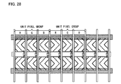
- the present liquid crystal panel can also be arranged such that in case where each pixel is grouped into pixel groups each consisting of a trio of pixels respectively corresponding to red, green, and blue disposed sequentially along a scanning signal line, the first alignment controlling structure provided on a pixel of a color belonging to one pixel group has a shape which is obtained by rotating by 180° the first alignment controlling structure provided on a pixel of the same color belonging to a pixel group adjacent to the pixel group.
- parts of first subpixels of the same color adjacent in the row direction e.g., two bright subpixels of the same color adjacent in the row direction
- viewing angle characteristic can be more improved.
- the present liquid crystal panel can also be arranged such that in a case where the direction along the scanning signal lines is referred to as the row direction, the first subpixel region has two end portions along the row direction, and the first alignment controlling structure includes at least one of (i) a V-shaped rib which is provided on the counter substrate and which is superposed on both of the two end portions of the first subpixel region and bent between the end portions in the row direction, (ii) a slit which is formed on the pixel electrode and V-shaped when viewed in the row direction, and (iii) a slit which is formed on the common electrode provided on the counter electrode and which is V-shaped when viewed in the row direction.
- the present liquid crystal panel can also be arranged such that in each pixel having the switching element which is provided between adjacent first and second data signal lines and connected to the first data signal line, each of the first and second alignment controlling structures of the pixel includes at least one of (i) the rib which is V-shaped when viewed in the row direction from the second data signal line, (ii) the slit which is formed on the pixel electrode and V-shaped when viewed in the row direction from the second data signal line, and (iii) the slit which is formed on the common electrode and V-shaped when viewed in the row direction from the second data signal line.
- the present liquid crystal panel may be arranged such that: the first transistor has a drain electrode connected to the first pixel electrode via a first drain drawing wiring and a first contact hole, and the second transistor has a drain electrode connected to the second pixel electrode via a second drain drawing wiring and a second contact hole; and at least parts of the first and second drain drawing wirings superpose the first and second alignment controlling structures, respectively. Furthermore, the present liquid crystal panel may also be arranged such that at least parts of the first and second contact holes superpose the first and second alignment controlling structures, respectively. With this, in a case where each alignment controlling structure is a light-blocking type, aperture ratio can be improved.
- the present liquid crystal panel may also be arranged such that: each first storage capacitor wiring has a first storage capacitor wiring extending section and each second storage capacitor wiring has a second storage capacitor wiring extending section, wherein the first storage capacitor wiring extending section is extended to the first pixel electrode to which the first storage capacitor wiring corresponds, and the second storage capacitor wiring extending section is extended to the second pixel electrode to which the second storage capacitor wiring corresponds; and at least parts of the first and second storage capacitor wiring extending sections superpose the first and second alignment controlling structures, respectively.
- aperture ratio can be maintained and a storage capacitor can be increased by each storage capacitor wiring extending section.
- the present liquid crystal panel may also be arranged such that: the first transistor has a drain electrode connected to the first pixel electrode via a first drain drawing wiring and a first contact hole, and the second transistor has a drain electrode connected to the second pixel electrode via a second drain drawing wiring and a second contact hole; and each first drain drawing wiring has a first superposition section superposed on the first storage capacitor wiring extending section and each second drain drawing wiring has a second superposition section superposed on the second storage capacitor wiring extending section.
- the first storage capacitor wiring extending section and the first drain drawing wiring can be connected together by penetrating an insulating film under the first superposition section.
- the first pixel electrode which is present in a defective pixel and the first storage capacitor wiring can be connected together via the first storage capacitor wiring extending section. This makes it possible to reduce a potential of the first pixel electrode to a potential of the first storage capacitor wiring.
- the present liquid crystal panel is desirably arranged such that: the first alignment controlling structure has a slit formed on the first pixel electrode, and the second alignment controlling structure has a slit formed on the second pixel electrode; and the first and second contact holes are formed (i) between the first superposition section and the first drain electrode and (ii) between the second superposition section and the second drain electrode, respectively; and each first drain drawing wiring has a part between the first drain electrode and the first contact hole, which part superposes any of the slits, and each second drain drawing wiring has a part between the second drain electrode and the second contact hole, which part superposes any of the slits.
- the present liquid crystal panel may also be arranged such that: the first transistor has a drain electrode connected to the first pixel electrode via a first drain drawing wiring and one or more contact holes and the second transistor has a drain electrode connected to the second pixel electrode via a second drain drawing wiring and one or more contact holes; and each first drain drawing wiring is hollowed where the first drain drawing wiring intersects with the contact hole and each second drain drawing wiring is hollowed where the second drain drawing wiring intersects with the contact hole.
- aperture ratio can be improved by the hollow.
- redundancy can be secured in terms of electric connection of the drain drawing wiring and each pixel electrode and thus poor connection can be prevented.
- the present liquid crystal panel may also be arranged such that: in a case where directions along the data signal line and the scanning signal line are referred to as row and column directions, respectively, each first drain drawing wiring is hollowed by having two hollows corresponding to two of the contact holes, the two hollows being extended in the row and column directions, respectively; and each second drain drawing wiring is hollowed by having two hollows corresponding to two of the contact holes, the two hollows being extended in the row and column directions, respectively.
- each first drain drawing wiring is hollowed by having two hollows corresponding to two of the contact holes, the two hollows being extended in the row and column directions, respectively
- each second drain drawing wiring is hollowed by having two hollows corresponding to two of the contact holes, the two hollows being extended in the row and column directions, respectively.
- a liquid crystal display unit of the present invention includes a liquid crystal panel as set forth above; and a driver.
- a liquid crystal display of the present invention includes a liquid crystal display unit as set forth above.
- the present liquid crystal display is arranged such that the scanning lines and the data signal lines are driven so that during one frame period, a signal potential having the negative polarity with respect to a standard potential is supplied to the switching elements in the vicinity of the intersections belonging to the A group and on the other hand, a signal potential having the positive polarity with respect to the standard potential is supplied to the switching elements in the vicinity of the intersections belonging to the B group.
- each dot (pixel) can be inversed. That is, the data signal line can be sufficiently charged by the nH/1V inversion driving, and the irregular disposition of bright subpixels as shown in Fig. 37 will not occur. With this, a liquid crystal display of high display quality in which display is less likely to be uneven can be realized.
- an inversion cycle of the data signal can be made longer (the data signal can be inversed for every n horizontal period). Therefore, moving picture performance can also be improved by performing pseudo impulse driving or writing an interpolation image with the frequency of image writing increased.
- nH/1V inversion driving can be applied, power consumption in a driver can be reduced and thus generation of heat in the driver can be prevented.
- a driver IC can be miniaturized. With this, an overall size of a liquid crystal display can also be reduced.
- the present liquid crystal display may also be arranged such that potentials of the first and second storage capacitor wirings are controlled so that phases of potential waveform of the first and second storage capacitor wirings are shifted by 180°.
- the present liquid crystal panel may also be arranged such that: each first storage capacitor wiring is controlled in potential such that the potential rises after each of the transistors is switched off and the rise state is maintained until each of the transistors is switched off in the next frame and on the other hand, each second storage capacitor wiring is controlled in potential such that the potential falls after each of the transistors is switched off and the fall state is maintained until each of the transistors is switched off in the next frame; or each first storage capacitor wiring is controlled in potential such that the potential falls after each of the transistors has been switched off and the fall state is maintained until each of the transistors is switched off in the next frame and on the other hand, each second storage capacitor wiring is controlled in potential such that the potential rises after each of the transistors has been switched off and the rise state is maintained until each of the transistors is switched off in the next frame.
- the present liquid crystal display may also be arranged such that potential rises of the first storage capacitor wiring and potential falls of the second storage capacitor wiring are shifted by one horizontal period, or potential falls of the first storage capacitor wiring and potential rises of the second storage capacitor wiring are shifted by one horizontal period.
- the present liquid crystal display can also be described as a liquid crystal display including pixel regions disposed in row and column directions where the row direction is an extending direction of a scanning signal line, each pixel region has a pair of pixel electrodes connected to the same one of the scanning signal lines and to the same one of the data signal lines via a switching element wherein the pixel electrodes form capacitors with storage capacitor wirings in such a manner that pixel electrodes in one pixel region form the capacitors with different ones of the storage capacitor wirings, respectively, and one of two pixel electrodes provided on one pixel region and one of the two pixel electrodes provided on a pixel region adjacent to the pixel region in the column direction, form the capacitors with the same one of the storage capacitor wirings, wherein each of two pixel electrodes provided on each pixel region in the same pixel region array is connected to one or the other of two adjacent data signal lines and n consecutive pixel regions are sequentially grouped into blocks in the same pixel region array where n ⁇ 2, for pixel regions belonging to the same block,
- the present liquid crystal display is desirably arranged such that the data signal lines are supplied alternatively with a signal potential equal to or higher than a standard potential and a signal potential equal to or lower than the standard potential for every n horizontal period in such a manner that one data signal line is supplied with one of the signal potentials in one horizontal period, while a data signal line adjacent to the data signal line is supplied with the other one of the signal potentials in the horizontal period.
- the present liquid crystal display may also be arranged such that: storage capacitor wiring signals whose levels are alternated in accordance with a cyclic level shift are supplied to the storage capacitor wirings in such a manner that two storage capacitor wirings forming the capacitors with the pair of pixel electrodes in one pixel region are supplied respectively with storage capacitor wiring signals which are alternative to each other in terms of the levels initially after a scanning signal line to which the pair of the pixel electrodes is connected is scanned.
- a television receiver of the present invention includes a liquid crystal display as set forth above; and a tuner section for receiving television broadcast.
- each dot (pixel) can be inversed when the data signal line is operated by the nH/1V inversion driving. That is, with the nH/1V inversion driving, the data signal line can be sufficiently charged and bright subpixels can be regularly disposed. With this, a liquid crystal display of high display quality in which display is less likely to be uneven can be realized. This effect may be particularly remarkable in a large-scale liquid crystal display.
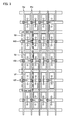
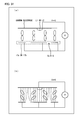
- Fig. 1 is a plan view of a liquid crystal panel according to an embodiment of the present invention. It should be noted that though the present liquid crystal panel includes an active matrix substrate of the present invention, a liquid crystal layer, and a color filter substrate, Fig. 1 does not show the liquid crystal layer and the color filter substrate.
- Fig. 2 is an enlarged plan view showing a part of Fig. 1 .
- the present active matrix substrate includes data signal lines 15 and scanning signal lines 16 which intersect at right angles to each other, first and second storage capacitor wirings 18a and 18b, and pixel regions 5 provided in a matrix pattern.
- a layer in which the data signal lines 15 are provided is higher than a layer in which the scanning signal lines 16 are provided.
- Each scanning signal line 16 extends in a row direction (horizontal direction in the drawing) so as to cross the pixel regions 5.
- Each data signal line 15 extends in a column direction (vertical direction in the drawing) along one side of pixel regions (edge along a direction in which the data signal line 15 intersects at right angles to the scanning signal lines 16).
- the first or second storage capacitor wiring 18a or 18b extends in the row direction (horizontal direction in the drawing) so as to superpose adjacent end portions of two pixel regions adjacent in the column direction.
- a switching element 12 including first and second transistors 12a and 12b, first and second pixel electrodes 17a and 17b, the first and second storage capacitor wirings 18a and 18b, first and second drain drawing wirings 27a and 27b, and first and second contact holes 11a and 11b are formed.
- the first and second pixel electrodes 17a and 17b are disposed on one (upper in the drawing) and the other (lower in the drawing) sides of the scanning signal line 16, respectively.
- the switching element 12 is provided in the vicinity of an intersection of the data signal line 15 and the scanning signal line 16.
- each of the first and second pixel electrodes 17a and 17b provided in any of the pixel regions 5 is connected to either of two data signal lines 15 on either side of the pixel region 5 via the switching element 12.
- a source electrode 9a of the first transistor is drawn in the row direction from the data signal line 15.
- a drain electrode 8a of the first transistor is formed so as to face the source electrode 9a and connected to the first pixel electrode 17a via the first drain drawing wiring 27a and the contact hole 11a.
- a first storage capacitor is formed on a superposition section in which the first pixel electrode 17a and the first storage capacitor wiring 18a superpose each other.
- a source electrode 9b of the second transistor is drawn in the row direction from the data signal line 15.
- a drain electrode 8b of the second transistor is formed so as to face the source electrode 9b.
- the drain electrode 8b is connected to the second pixel electrode 17b via the second drain drawing wiring 27b and the contact hole 11b.
- a second storage capacitor is formed on a superposition section in which the second pixel electrode 17b and the second storage capacitor wiring 18b superpose each other.
- each pixel is formed in such a manner that (i) it is formed with the pixel region 5, and regions on a color filter substrate and in a liquid crystal layer which regions correspond to the pixel region 5, (ii) a first subpixel is formed with a region on which the first pixel electrode 17a is provided, and regions on the counter substrate and in the liquid crystal layer which regions correspond to the region on which the first pixel electrode 17a is provided, and (iii) a second subpixel is formed with a region on which the second pixel electrode 17b is provided, and regions on the counter substrate and in the liquid crystal layer which regions correspond to the region on which the second pixel electrode 17b is provided.
- the same signal potential is supplied from the data signal line 15 to the first or second pixel electrodes 17a or 17b.
- potentials of the first and second storage capacitor wirings 18a and 18b are individually controlled so as to set the first and second pixel electrodes 17a and 17b to different potentials via the first and second storage capacitors.
- a liquid crystal display including the present liquid crystal panel constituting each pixel by a high-luminance subpixel (bright subpixel) and a low-luminance subpixel (dark subpixel) makes it possible to display halftone by area coverage modulation and thus viewing angle dependence of ⁇ characteristic (e.g. excess brightness) can be improved.
- ⁇ characteristic e.g. excess brightness
- Figs. 1 , 3 and 4 the following describes a relationship of connection of first and second pixel electrodes which are provided in each pixel region on an active matrix substrate of the present liquid crystal panel to a data signal line.
- a liquid crystal panel is applied to a liquid crystal display in which the nH/1V inversion driving as set forth above is performed.
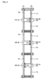
- Fig. 3 is a schematic view showing a part of the aforementioned active matrix substrate
- Fig. 4 is an enlarged plan view showing a part of Fig. 3 , which part is enclosed with a bold dashed line in Fig. 3 .
- intersections of the same data signal line and the scanning signal lines are alternately grouped into A and B groups for every n (n: not less than 2) adjacent intersections and intersections adjacent in the row direction are grouped into different groups, thereby the intersections of the data signal lines and the scanning signal lines are grouped into the A and B groups.
- Fig. 3 shows a case where n is 2 (that is, a case where a liquid crystal panel is applied to a liquid crystal display in which the 2H/1V inversion driving is performed).
- each of the first and second pixel electrodes 17a and 17b provided in any of the pixel regions is connected: (i) to a first data signal line, which is one of two data signal lines on either side of the pixel region, via the switching element 12 provided in the vicinity of the intersection of the first data signal line and the scanning signal line 16 crossing the pixel region; or (ii) to a second data signal line, which is the other of the two data signal lines on either side of the pixel region, via the switching element 12 provided in the vicinity of the intersection of the second data signal line and the scanning signal line 16 crossing the pixel region.
- a pixel region as above and two data signal lines on either side thereof are referred to as a pixel region 5S and first and second data signal lines 15x and 15y, respectively, as shown in Figs. 3 and 4 .
- Two pixel electrodes (17a and 17b) provided on the pixel region 5S are connected to the first data signal line 15x via a switching element 12x provided in the vicinity of an intersection 20Sx of a scanning signal line 16S crossing the pixel region 5S and the first data signal line 15x.
- the intersection 20Sx belongs to the A group.
- a pixel region adjacent to the pixel region 5S in the column direction is referred to as an adjacent pixel region.
- an intersection of the scanning signal line crossing the adjacent pixel region and the first data signal line 15x and (ii) the intersection 20Sx of the scanning signal line 16S crossing the pixel region 5S and the first data signal line 15x belong to the same group (A)
- two pixel electrodes included in this adjacent pixel region are both connected to the second data signal line 15y via the switching element.
- an active matrix substrate of the present liquid crystal panel can be configured.
- Fig. 20 shows a case where n is 3 (i.e., a case where a liquid crystal panel is applied to a liquid crystal display in which 3H/1V inversion driving is performed).
- Fig. 5 is a schematic view showing part of a display region of the present liquid crystal display.
- Fig. 6 is an enlarged plan view showing a part of Fig. 5 , which part is enclosed with a bold dashed line in Fig. 5 .
- the negative and positive polarities are supplied to (i) the switching element which is in the vicinity of the intersection belonging to the A group and (ii) the switching element which is in the vicinity of the intersection belonging to the B group, respectively.
- potentials of adjacent storage capacitor wirings are reversely fluctuated in such a manner that: a rising potential is supplied to a storage capacitor wiring 18 ⁇ ; a falling potential is supplied to a storage capacitor wiring 18 ⁇ adjacent to the storage capacitor wiring 18 ⁇ ; the rising potential is supplied to a storage capacitor wiring 18 ⁇ adjacent to the storage capacitor wiring 18 ⁇ ; and the falling potential is supplied to a storage capacitor wiring 18 ⁇ adjacent to the storage capacitor wiring 18 ⁇ (potential control of the storage capacitor wiring is to be described in details later).
- the display as shown in Fig. 5 is performed.
- a first subpixel of a pixel 5q is a bright subpixel since the subpixel is under potential rise by the storage capacitor wiring 18 ⁇ after positive polarity is written from the data signal line 15x.
- a second subpixel of the pixel region 5q is a dark subpixel since the subpixel is under potential fall by the storage capacitor wiring 18 ⁇ after positive polarity is written from the data signal line 15x.
- a first subpixel of a pixel 5s is a bright subpixel since the subpixel is under potential fall by the storage capacitor wiring 18 ⁇ after the negative polarity is written from the data signal line 15x.
- a second subpixel of the pixel region 5s is a dark subpixel since the subpixel is under potential rise by the storage capacitor wiring 18 ⁇ after the negative polarity is written from the data signal line 15x.
- a first subpixel of a pixel 5p is a bright subpixel since the subpixel is under potential rise by the storage capacitor wiring 18 ⁇ after the positive polarity is written from the data signal line 15y.
- a second subpixel of the pixel region 5p is a dark subpixel since the subpixel is under potential fall by the storage capacitor wiring 18 ⁇ after the positive polarity is written from the data signal line 15y.
- each dot (pixel) is inverted as shown in Fig. 5 and dots are not irregularly disposed as shown in Fig. 37 . With this, even and clear display can be realized.
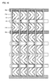
- the present liquid crystal panel can also be configured by MVA (Multidomain Vertical Alignment) as shown in Fig. 7 .
- MVA Multidomain Vertical Alignment
- Fig. 7 does not show the liquid crystal layer but shows a rib only for the color filter substrate.
- Fig. 8 (a) is an enlarged plan view showing a part of Fig. 7 .
- first and second subpixel regions are provided so as to sandwich the scanning signal line 16 therebetween.
- First and second subpixels are configured to include: (i) the first subpixel region and a region on a color filter substrate which region corresponds to the first subpixel region and (ii) the second subpixel region and a region on the color filter substrate which region corresponds to the second subpixel region, respectively.
- the first subpixel is provided with the first pixel electrode 17a superposed on almost all the first subpixel region.
- the first subpixel is further provided with a first alignment controlling structure including a first rib L1 and slits (pixel electrode slits) S1 to S4.
- the second subpixel is provided with the second pixel electrode 17b superposed on almost all the second subpixel region.
- the second subpixel is further provided with a second alignment controlling structure including a second rib L2 and slits (pixel electrode slits) S5 to S8. Then one pixel 55 is constituted by the first and second subpixels.
- the first subpixel located on one side of the scanning signal line 16 has an end portion E1 along the scanning signal line 16 and an end portion E2 facing the end portion E1 and the second subpixel located on the other side of the scanning signal line 16 has an end portion E1 along the scanning signal line 16 and an end portion E2 facing the end portion E1.
- the region on the color filter substrate which region corresponds to the first subpixel is provided with the first rib L1 which is V-shaped when viewed in the row direction (in a direction from the left to the right in the drawing) so that a start section T and a termination section M are located on the end portions E1 and E2, respectively.
- the region on the color filter substrate which region corresponds to the second subpixel is provided with the second rib L2 which is V-shaped when viewed in the row direction (in the direction from the left to the right in the drawing) so that a start section T and a termination section M are located on the end portions E1 and E2, respectively. That is, the first rib L1 and the second rib L2 are provided in the same direction.
- a plurality of slits S1 to S4 are provided in the first pixel electrode 17a so as to correspond to the first rib L1.
- a plurality of slits S5 to S8 are provided in the second pixel electrode 17b so as to correspond to the second rib L2.
- the slits S2 and S4 are provided on either side of a segment of the first rib L1 from the start section T to a bend section K so as to be substantially parallel to the segment.
- the slits S1 and S3 are provided on either side of a segment of the first rib L1 from the bend section K to the termination section M so as to be substantially parallel to this segment.
- the slits S5 and S7 are provided on either side of a segment of the second rib L2 from the start section T to a bend section K so as to be substantially parallel to this segment.
- the slits S6 and S8 are provided on either side of a segment of the second rib L2 from the bend section K to the termination section M so as to be substantially parallel to this segment.
- the slits S5 to S8 are similar to the slits S1 to S4 in shape and where to dispose the slits S5 to S8 with respect to the second rib L2 is similar to where to dispose the slits S1 to S4 with respect to the first rib L1. It should be noted that for the first or second rib L1 or L2, an angle formed by the start section T, the bend section K, and the termination section M ( ⁇ TKM) is about 90°.
- the slit S1, one side of the first rib L1 (the segment KM), and the slit S3 are parallel to each other and obliquely stretch with respect to the scanning signal line 16 (at an angle of about 45°).
- the slit S2, one side of the first rib L1 (the segment TK), and the slit S4 are parallel to each other and obliquely stretch with respect to the scanning signal line 16 (at an angle of about 135°).
- a portion of the one side of the first rib L1 (the segment TK) and a portion of the slit S4 are located on the end portion (along the scanning signal line 16) of the first subpixel.
- the slit S6, one side of the second rib L2 (the segment KM), and the slit S8 are parallel to each other and obliquely stretch with respect to the scanning signal line 16 (at an angle of about 135°).
- the slit S5, one side of the second rib L2 (the segment TK), and the slit S7 are parallel to each other and obliquely stretch with respect to the scanning signal line 16 (at an angle of about 45°).
- a portion of the one side of the second rib L2 (the segment TK) and a portion of the slit S7 are located on the end portion (along the scanning signal line 16) of the second subpixel.
- alignment regions D3 and D4 are formed on either side of the segment of the first rib L1 from the start section T and to bend section K and alignment regions D1 and D2 are formed on either side of the segment of the first rib L1 from the bend section K to the termination section M, as shown in Fig. 8 (b) .
- the alignment regions D1 to D4 are formed as follows: The alignment region D2 is formed on a side of the slit S1 which side faces away from the first rib L1; The alignment region D3 is formed on a side of the slit S2 which side faces away from the first rib L1; The alignment region D1 is formed on a side of the slit S3 which side faces away from the first rib L1; The alignment region D4 is formed on a side of the slit S4 which side faces away from the first rib L1.
- alignment regions D1 and D2 are formed on either side of the segment of the second rib L2 from the start section T to the bend section K and alignment regions D3 and D4 are formed on either side of the segment of the second rib L2 from the bend section K to the termination section M, as shown in Fig. 8 (b).
- the alignment regions D1 to D4 are formed as follows: The alignment region D2 is formed on a side of the slit S5 which side faces away from the second rib L2; The alignment region D3 is formed on a side of the slit S6 which side faces away from the second rib L2; The alignment region D1 is formed on a side of the slit S7 which side faces away from the second rib L2; The alignment region D4 is formed on a side of the slit S8 which side faces away from the second rib L2. With this, a broader viewing angle can be realized in a liquid crystal display to which the present liquid crystal panel is applied.
- the first alignment controlling structure (rib and slits) provided on a pixel 55x which is one of two pixels 55x and 55y adjacent in the column direction has a shape which is obtained by rotating by 180° the first alignment controlling structure (rib and slits) provided on the pixel 55y which is the other of the two pixels 55x and 55y adjacent in the column direction.
- the first and second alignment controlling structures are substantially identical in shape. Accordingly, the second alignment controlling structure (rib and slits) provided on the pixel 55x has a shape which is obtained by rotating by 180° the second alignment controlling structure (rib and slits) provided on the pixel 55y.
- ribs L11 and L12, first and second pixel electrodes 17c and 17d, and slits S11 to S18, each of which is provided on the pixel 55y can be obtained by rotating by 180° the ribs L1 and L2, the first and second pixel electrodes 17a and 17b, and the slits S1 to S8, each of which is provided on the pixel 55x.
- the slit S11, one side of the first rib L11, and the slit S13 are parallel to each other and obliquely stretch with respect to the scanning signal line 16 (at an angle of about 135°).
- the slit S12, one side of the first rib L11, and the slit S14 are parallel to each other and obliquely stretch with respect to the scanning signal line 16 (at an angle of about 45°).
- a portion G of the one side of the first rib L1 and a portion H of the slit S4 are located on the end portion (along the scanning signal line 16) of the first subpixel.
- the slit S16, one side of the second rib L12, and the slit S18 are parallel to each other and obliquely stretch with respect to the scanning signal line 16 (at an angle of about 45°).
- the slit S15, one side of the second rib L12, and the slit S17 are parallel to each other and obliquely stretch with respect to the scanning signal line 16 (at an angle of about 135°).
- a portion I of the one side of the second rib L12 (the segment TK) and a portion J of the slit S17 are located on the end portion (along the scanning signal line 16) of the second subpixel.
- the pixel 55x as shown in Fig.
- a portion B of the one side of the first rib L1 and a portion A of the slit S4 are located on the end portion of the first subpixel (along the scanning signal line 16) and a portion F of the one side of the second rib L2 and a portion C of the slit S7 are located on the end portion of the second subpixel (along the scanning signal line 16).
- Fig. 9 (b) shows the distribution of the alignment regions D1 to D4 formed on the pixels 55x and 55y. It should be noted that in each of the pixels 55x and 55y, the first and second subpixels correspond to bright and dark subpixels, respectively.
- parts of random alignment in the alignment regions D1 to D4 of the bright and dark subpixels in the two adjacent pixels 55x and 55y are as follows: Parts of random alignment in the alignment regions D1 to D4 of the bright subpixel in the pixel 55x are 0 (none), 0 (none), XM3, and XM4 ⁇ + XM4 ⁇ , respectively. Parts of random alignment in the alignment regions D1 to D4 of the dark subpixel in the pixel 55x are XA1 ⁇ + XA1 ⁇ , XA2, 0 (none), and 0 (none), respectively.
- Parts of random alignment in the alignment regions D1 to D4 of the bright subpixel in the pixel 55y are YM1, YM2 ⁇ + YM2 ⁇ , 0 (none), and 0 (none), respectively.
- Parts of random alignment in the alignment regions D1 to D4 of the dark subpixel in the pixel 55y are 0 (none), 0 (none), YA3 ⁇ + YA3 ⁇ , and YA4, respectively.
- parts of random alignment in the alignment regions D1 to D4 which parts are included in two bright subpixels are YM1, YM2 ⁇ + YM2 ⁇ , XM3, and XM4 ⁇ + XM4 ⁇ , respectively.
- parts of random alignment in the alignment regions D1 to D4 which parts are included in two dark subpixels are XA1 ⁇ + XA1 ⁇ , XA2, YA3 ⁇ + YA3 ⁇ , and YA4, respectively.
- the above shows that in the present liquid crystal panel, the parts of random alignment to which the two bright subpixels included in the pixels 55x and 55y adjacent in the column direction is subjected are diluted over the alignment regions D1 to D4. Furthermore, in the present liquid crystal panel, the first and second alignment controlling structures are provided in the pixels 55x and 55y so that YM1, YM2 ⁇ + YM2 ⁇ , XM3, and XM4 ⁇ + XM4 ⁇ are substantially equal in size. Therefore, areas of random alignment in the alignment regions D1 to D4 are (influence of random alignment to which the alignment regions are subjected is) almost equalized.
- the parts of random alignment to which the two dark subpixels included in the pixels 55x and 55y adjacent in the column direction is subjected are diluted over the alignment regions D1 to D4.
- the first and second alignment controlling structures are provided in the pixels 55x and 55y so that XA1 ⁇ + XA1 ⁇ , XA2, YA3 ⁇ + YA3 ⁇ , and YA4 are substantially equal in size. Therefore, areas of random alignment in the alignment regions D1 to D4 are (influence of random alignment to which the alignment regions are subjected is) almost equalized.
- the above is also applied to a case where bright and dark subpixels are replaced with each other in each pixel.
- the sizes of the parts of random alignment can be approximated to lengths on the scanning signal line 16 which are shown in Fig. 9 (a) as follows: YM1, YM2 ⁇ , YM2 ⁇ , XM3, XM4 ⁇ , XM4 ⁇ , XA1 ⁇ , XA1 ⁇ , XA2, YA3 ⁇ , YA3 ⁇ , and YA4 can be approximated to lengths between: G and H, P and G, H and Q, A and B, P and A, B and Q, P and C, F and Q, C and F, P and I, J and Q, and I and J, respectively.
- P and Q show either edge of the subpixel along the scanning signal line.
- the ribs L1 and L2 of the two pixels adjacent in the column direction are reversely provided. Therefore, influence of the part of random alignment along the scanning signal line 16 is diluted over the alignment regions D1 to D4. This makes it possible not to cause a large difference to viewing angle characteristic in each direction.
- the first and second ribs are separate (independent from each other with a gap therebetween). Therefore, for example, in a case where a one drop filling process (described later) is practiced, production of vacuum bubbles in liquid crystals can be prevented. This is because the gap between the first and second ribs facilitates the spread of liquid crystals. Furthermore, also in a case where an alignment film is formed by an ink-jet technique, the gap between the first and second ribs facilitates the spread of the alignment film. This makes it possible to prevent the alignment film from being unevenly formed.
- liquid crystal panel shown in Figs. 7 and 8 (a) can also be arranged such that the first and second ribs L1 and L2 are connected together by a rib Lc provided so as to be superposed on the scanning signal line 16, as shown in Fig. 29 .
- a zigzag rib is provided on one pixel.
- the present liquid crystal panel can also be arranged as Fig. 30 .
- the first and second ribs L1 and L2 in Fig. 8 (a) are replaced with first and second common electrode slits (slits provided on common electrodes) Sp and Sq, respectively.
- the liquid crystal panel of Fig. 30 is arranged similarly to that of Fig. 8 (a) .
- liquid crystal molecules are tilted in different directions with respect to each region partitioned with (i) the first common electrode slit Sp and each slit S formed on the first pixel electrode 17a or (ii) the second common electrode slit Sq and each slit S formed on the second pixel electrode 17b (a dashed line in Fig. 31 (b) shows an electrical flux line).
- four alignment regions are formed in each of the first and second subpixels (similarly to Fig. 9 (b) ).
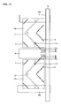
- the present liquid crystal panel may also be arranged such that in each pixel, a rib is directed toward where the switching element 12 is connected. That is, as shown in Figs. 11 and 12 , the ribs L1 and L2 are provided on the pixel 55 which is located between the adjacent data signal lines 15x and 15y and has the switching element 12 connected to the data signal line 15x.
- the ribs L1 and L2 are arranged such that the start sections T and the termination sections H thereof are closer to the data signal line 15x than the bend sections K thereof. With this, most parts of the first and second drain drawing wirings 27a and 27b can be formed under the first and second ribs L1 and L2, respectively. Therefore, aperture ratio of the pixel 55 can be improved.
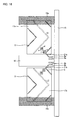
- Fig. 19 shows a cross-sectional view taken along the line Y of Fig. 11 .
- the scanning signal line 16 and a storage capacitor wiring (not illustrated) are formed on a substrate 31.
- the first drain drawing wiring 27a is formed via a gate insulating film 23.
- the first pixel electrode 17a is formed via an interlayer insulating film 25.
- an alignment film 9 is formed so as to cover the first pixel electrode 17a.
- the interlayer insulating film 25a is removed and the first drain drawing wiring 27a and the first pixel electrode 17a are connected together.
- a color filter substrate 30 faces the active matrix substrate 3 via a liquid crystal layer 40.
- a color filter 14 positioned to correspond to the pixel electrode 17a and a black matrix 13 closing a gap between color filters 14are formed.
- a counter electrode 28 is formed on the color filter 14 and the black matrix 13.
- a rib L is formed on a part of the counter electrode 28.
- an alignment film 19 is formed so as to cover the counter electrode 28 and the rib L.
- the present liquid crystal panel may also be arranged as shown in Fig. 13 . That is, a first storage capacitor wiring extending section 38a extends from the first storage capacitor wiring 18a so as to superpose the first pixel electrode 17a on the first storage capacitor wiring extending section 38a. On the other hand, a second storage capacitor wiring extending section 38b extends from the second storage capacitor wiring 18b so as to superpose the second pixel electrode 17b on the second storage capacitor wiring extending section 38b.
- the first and second storage capacitor wiring extending sections 38a and 38b superpose the first and second ribs L1 and L2, respectively.
- the first drain drawing wiring 27a has a first superposition section 33a to be superposed on the first storage capacitor wiring extending section 38a.
- the second drain drawing wiring 27b has a second superposition section 33b to be superposed on the second storage capacitor wiring extending section 38b. Moreover, most parts of the first and second drain drawing wirings 27a and 27b are formed under the first and second ribs L1 and L2, respectively.
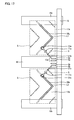
- Fig. 18 shows a cross-sectional view taken along the line x of Fig. 13 .
- the scanning signal line 16 and the first storage capacitor wiring extending section 38a are formed on the substrate 31.
- the first drain drawing wiring 27a is formed via the gate insulating film 23.
- the first pixel electrode 17a is formed via the interlayer insulating film 25.
- the alignment film 9 is formed so as to cover the first pixel electrode 17a.
- the color filter substrate 30 faces the active matrix substrate 3 via the liquid crystal layer 40.
- the color filter 14 positioned to correspond to the pixel electrode 17a and the black matrix 13 closing a gap between color filters 14 are formed.
- the counter electrode 28 is formed on the color filter 14 and the black matrix 13, the counter electrode 28 is formed.
- the rib L is formed on the part of the counter electrode 28.
- the alignment film 19 is formed so as to cover the counter electrode 28 and the rib L. Under the rib L, a part of the first drain drawing wiring 27a (the first superposition section) is superposed on a part of the first storage capacitor wiring extending section 38a via the gate insulating film 23.
- the first storage capacitor wiring extending section 38a and the first drain drawing wiring 27a can be connected together by penetrating the insulating film under the first superposition section 33a.
- the drain drawing wiring 27a can be disconnected between the first contact hole 11a and the first drain electrode 8a.
- the first pixel electrode 17a which is present in a defective pixel and the first storage capacitor wiring 18a can be connected together via the first storage capacitor wiring extending section 38a. This makes it possible to reduce a potential of the first pixel electrode 17a to a potential of the first storage capacitor wiring 18a.
- a defective pixel in which malfunction has occurred can be less noticeable by changing the defective pixel into a black dot.
- the liquid crystal panel shown in Fig. 10 can also be modified as shown in Fig. 14 . That is, the ribs are reversely provided with respect to each pixel for the column direction (up and down direction in the drawing), without the need of changing a shape of each switching element 12.
- a pixel in which the rib is directed toward where the switching element 12 is connected is as shown in Fig. 11 .
- a pixel in which the rib is not directed toward where the switching element 12 is connected is as shown in Fig. 15 .
- the drain drawing wirings 27a and 27b and the contact holes 11a and 11b are positioned where no rib and slit are provided thereon and thereunder. Then as shown in Fig.
- a hollow 99a or 99b intersecting with corresponding one of the contact holes 11a and 11b is formed on corresponding one of the drain drawing wirings 27a and 27b.
- the present liquid crystal panel may also be arranged as shown in Fig. 16 . That is, two contact holes c and d are formed on the drain drawing wiring 27a. Furthermore, a extended hollow e or f intersecting at right angles to corresponding one of the contact holes c and d is formed on the drain drawing wiring 27a. It should be noted that one and the other of the hollows extend in the column and row directions, respectively. With this, such an effect that an area of contact is unlikely to be reduced can be achieved even if random alignment occurs.
- the present liquid crystal panel can be arranged as shown in Fig. 17 . That is, the first storage capacitor wiring extending section 38a extends from the first storage capacitor wiring 18a so as to superpose the first pixel electrode 17a on the first storage capacitor wiring extending section 38a.
- the second storage capacitor wiring extending section 38b extends from the second storage capacitor wiring 18b so as to superpose the second pixel electrode 17b on the second storage capacitor wiring extending section 38b.
- the first and second storage capacitor wiring extending sections 38a and 38b superpose the first and second ribs L1 and L2, respectively.
- the first drain drawing wiring 27a has the first superposition section 33a to be superposed on the first storage capacitor wiring extending section 38a.
- the second drain drawing wiring 27b has the second superposition section 33b to be superposed on the second storage capacitor wiring extending section 38b.
- the first drain drawing wiring 27a has, between the second drain electrode 8a and the first contact hole 11a, a part on which the slit S is superposed.
- the second drain drawing wiring 27b has, between the second drain electrode 8b and the second contact hole 11b, a part on which the slit S is superposed.
- the first storage capacitor wiring extending section 38 and the first drain drawing wiring 27a can be connected together by penetrating the insulating film under the first superposition section 33a.
- the drain drawing wiring 27a can be disconnected between the first contact hole 11a and the first drain electrode 8a (under the slit S) where no pixel electrode is provided. This makes the disconnection process easy.
- the present liquid crystal panel may also be arranged as shown in Fig. 28 . That is, three pixels which correspond to red (R), green (G), and (B) and are disposed in the row direction are referred to as one pixel region group. For two pixel regions of the same color which are included in two pixel region groups adjacent in the row direction, each rib provided on one of the two pixel regions has a shape which is obtained by rotating by 180° each rib provided on the other of the two pixel regions. With this, in a liquid crystal display including the present liquid panel, for a pixel (two-pixel) unit of the same color, influence of the part of random alignment along the scanning signal line 16 is diluted over the alignment regions. This makes it possible not to cause a large difference to viewing angle characteristic in each direction.
- a sputtering technique so as to have a thickness of 1000 to 3000 ⁇ .
- Such a film is patterned by a photo-etching technique so as to be in the shape as required and thereby a scanning signal line (also serving as a gate electrode of each transistor) and a storage capacitor wiring are formed.
- a silicon nitride film (SiNx) serving as a gate insulating film (ii) a high-resistance semiconductor layer of amorphous silicon, polysilicon, or the like, and (iii) a low-resistance semiconductor layer of n + amorphous silicon or the like are sequentially formed by a plasma CVD (chemical vapor phase deposition) technique or the like. (i) to (iii) are patterned by the photo-etching technique.
- thicknesses of (i) the silicon nitride film as the gate insulating film, (ii) the amorphous silicon film as the high-resistance semiconductor layer, and (iii) the n + amorphous silicon film as the low-resistance semiconductor layer are about: 3000 to 5000 ⁇ , 1000 to 3000 ⁇ , and 400 to 700 ⁇ , respectively, for example.
- a metal film of titanium, chromium, aluminum, molybdenum, tantalum, tungsten, copper, or the like, (ii) an alloy film of these metals, or (iii) a laminated film in which the metal film or the alloy film is included is formed, by a method, such as the sputtering technique, so as to have a thickness of 1000 to 3000 ⁇ .
- a film is patterned by the photo-etching technique or the like so as to be in the shape as required and thereby a data signal line, a source electrode, a drain electrode, and a drain drawing wiring are formed.
- channel etching is performed by dry etching by making the data signal line, the source electrode, the drain electrode, and the drain drawing wiring in a mask pattern.
- a thickness of the i layer is optimized and each transistor (channel region) is formed.
- a semiconductor layer which is not covered with the data signal line, the source electrode, the drain electrode, and the drain drawing wiring is removed by etching and a thickness of the i layer which thickness is necessary for the capability of each transistor is left.
- an interlayer insulating film (i) a photosensitive acrylic resin film, (ii) an inorganic insulating film of silicon nitride, oxide silicon, or the like, (iii) a laminated film of the photosensitive acrylic resin film and the inorganic insulating film, or (iv) the like is formed so as to cover each transistor (channel region), the data signal line, the source electrode, the drain electrode, and the drain drawing wiring.
- the photosensitive acrylic resin film which has been formed by a spin coat technique and has a thickness of 20000 to 40000 ⁇ or (iii) a laminated film of the silicon nitride film and the photosensitive acrylic resin film can be applied.
- a silicon nitride film is formed as the interlayer insulating film (a passivation film).
- a polyimide resin film, a nonphotosensitive resin film, or a spin-on glass (SOG) film can also be applied as the interlayer insulating film.
- a hole is formed by etching the interlayer insulating film in accordance with a position of a contact hole.
- photosensitive resist is patterned by a photolithography technique (exposure and development) and the photosensitive resist is etched.
- a transparent conductive film of ITO (indium tin oxide), IZO, zinc oxide, tin oxide, or the like is formed so as to have a thickness of about 1000 to 2000 ⁇ by the sputtering technique or the like.
- the transparent conductive film is patterned by the photo-etching technique so as to be in the shape as required and thereby each pixel electrode is formed.
- each pixel electrode is formed so as to include a slit or the like.
- an alignment film is applied by the ink-jet technique or the like. According to the above steps, an active matrix substrate is formed.
- Liquid crystal may be filled by such a method (vacuum filling method) that: thermosetting sealing resin is provided with an inlet through which liquid crystal is filled; the inlet is soaked with liquid crystal in a vacuum; the liquid crystal is filled by releasing air; and thereafter the inlet is sealed with UV cure resin.
- liquid crystal may also be filled by a one drop filling process as described below.
- UV cure sealing resin including spacer, such as fiberglass is applied on the circumference of the active matrix substrate and liquid crystal is dropped on the color filter substrate by the one drop process.
- a suitable amount of liquid crystal can be regularly dropped in an inner part of the seal.
- the drop amount is determined by a cell gap value and a value of volume of a cell in which liquid crystal needs to be filled.
- atmosphere in a combining device is decompressed to 1Pa. Under such a decompressed state, the substrates are combined together. In this way, by making atmosphere to atmospheric pressure, a sealed part is crushed.
- UV is irradiated by a UV cure device so as to temporarily cure the sealing resin.
- the sealing resin is baked so as to be finally cured. At this point, liquid crystal is spread inside the sealing resin and the liquid crystal is filled in a cell.
- the color filter substrate On the color filter substrate, (i) colored layers (R, G, and B) disposed in a matrix pattern so as to correspond to each pixel of the active matrix substrate, (ii) a black matrix provided in a gap between the colored layers, (iii) a counter electrode (common electrode), and (iv) the like are formed.
- a color filter substrate By combining such a color filter substrate with the present active matrix substrate, and dropping and sealing liquid crystal as mentioned above, the present liquid crystal panel is formed.
- the present liquid crystal display unit and liquid crystal display are arranged as below.
- Fig. 27 to either side of a liquid crystal panel, two polarization plates A and B are combined so that polarization axes of the polarization plates A and B intersect at right angles to each other. Furthermore, an optical compensation sheet or the like may be laminated on the polarization plate if necessary.
- drivers a gate driver 102 and a source driver 101
- TCP Transmission Career Package
- TCP is positioned with respect to a panel terminal electrode, heated and finally pressed. Thereafter, a circuit substrate 103 (PWB: Printed wiring board) for connecting the drivers TCP together and an input terminal of TCP are connected together with ACF. With this, a liquid crystal display unit 100 is completed.
- PWB Printed wiring board
- a display control circuit 113 is connected to the drivers (101 and 102) of the liquid crystal display unit via the circuit board 103.
- an illumination device (backlight unit) 104 By integrating the liquid crystal display unit and the display control circuit 113 with an illumination device (backlight unit) 104, a liquid crystal display 110 is completed.
- Fig. 21 is a timing chart showing operation of each section in the present liquid crystal display.
- Vg, Vs, Vcs1, Vcs2, Vlc1, and Vlc2 are voltages of: the scanning line 16, the data line 15 (source voltage), the first storage capacitor wiring 18a, the second storage capacitor wiring 18b, the first pixel electrode 17a, and the second pixel electrode 17b, respectively.
- each of the voltages of the first and second storage capacitor wirings 18a and 18b is modulated with an amplitude voltage Vad and their phases are shifted by 180°. That is, just after Vg is L at T2 (the TFTs 12a and 12b are off), Vcs1 and Vcs2 are controlled to be H and L, respectively.
- Vcs1 can be waveform remaining High (or Low) at T3 just after Vg is L at T2 (the TFTs 12a and 12b are off) and Vcs2 can also be waveform remaining Low (or High) at T4 after one horizontal period (1H) from T3. That is, potentials are controlled in such a manner of: increasing Vcs1 after each transistor is off and maintaining the rise state in the frame, and decreasing Vcs2 after 1H period from the rise of Vcs1 and maintaining the fall state in the frame; or decreasing Vcs1 after each transistor is off and maintaining the fall state in the frame, and increasing Vcs2 after 1H period from the fall of Vcs1 and maintaining the rise state in the frame. With this, waveform distortion of Vcs1 and Vcs2 has less influence on drain effective potential and thus this is effective in reducing uneven luminance.
- Fig. 33 is a schematic view showing a relationship of connection of a pixel to each wiring (a data signal line, a scanning line, or a storage capacitor wiring) in the present liquid crystal display, and a method for driving the present liquid crystal display.
- Fig. 34 is a timing chart showing one example of the method for driving the present liquid crystal display.
- the present liquid crystal display includes the data signal lines (15Y and 15X), the scanning signal lines (G1 to G6), and the storage capacitor wirings (Cs1 to Cs6).
- the row direction horizontal direction in the drawing
- pixels enclosed with thin dashed lines are disposed in the row and column directions.
- two pixel electrodes provided on one pixel are connected to the same scanning signal and data signal lines via the switching element and form capacitors with different storage capacitor wirings.
- One of two pixel electrodes provided on one of two pixels adjacent in the column direction and one of the two pixel electrodes provided on the other of the two pixels form capacitors with the same storage wiring.
- two pixel electrodes provided on a pixel PX1 are connected to the scanning signal line G1 and the data signal line 15Y via the switching element, and form capacitors with different storage capacitor wirings (Cs1 and Cs2).
- One of two pixel electrodes provided on one (PX1) of two pixels adjacent in the column direction and one of the two pixel electrodes provided on the other (PX2) of the two pixels form capacitors with the same storage capacitor wiring (Cs2).
- two pixel electrodes provided on any pixel in the same pixel array are connected to one or the other of two adjacent data signal lines.
- the data signal line to which two pixel electrodes provided on one of the pixels are connected is different from the data signal line to which two pixel electrodes provided on the other of the pixels are connected.
- the data signal line to which two pixel electrodes provided on one of the pixels are connected is the same as the data signal line to which two pixel electrodes provided on the other of the pixels are connected.
- two pixel electrodes provided on any of the pixels (PX1 to PX5) in a pixel array PLj are connected to one (15Y) or the other (15X) of two adjacent data signal lines.
- the pixel array PLj when consecutive pixels PX1 and PX2 are blocked and thereafter pixels PX3 and PX4 are blocked, for the two pixels PX1 and PX2 belonging to the same block and being adjacent in the column direction, two pixel electrodes provided on one (PX1) of the pixels are connected to the data signal line 15Y and two pixel electrodes provided on the other (PX2) of the pixels are connected to the data signal line 15X.
- two pixel electrodes provided on one (PX2) of the pixels are connected to the data signal line 15X as mentioned above and two pixel electrodes provided on the other (PX3) of the pixels are also connected to the data signal line 15X.
- digital data DAT (15Y) corresponding to the data signal line 15Y of Fig. 33 , digital data DAT (15X) corresponding to the data signal line 15X of Fig. 33 , a signal potential Vs (15Y) to be supplied to the data signal line 15Y of Fig. 33 , a Cs signal (storage capacitor wiring signal) Scs1... to be supplied to the storage capacitor wiring Cs1 ... of Fig. 33 are set as shown in Fig. 34 , for example.
- H in Fig. 34 means a horizontal period (horizontal scanning period).
- Vs (15Y) and Vs (15X) can be obtained by analog conversion of DAT (15Y) and DAT (15X), respectively.
- DAT (15Y) and DAT (15X) are generated from (i) DAT (digital data) for pixel arrays PLi and PLj and (ii) DAT (digital data) for pixel arrays PLj and PLk, respectively.
- DAT digital data
- data corresponding to pixels PX1, PX4, and PX5 in the pixel array PLj is provided during the first, fourth, and fifth horizontal periods and data corresponding to pixels in the second, third, and sixth rows of the pixel array PLi is provided during the second, third, and sixth horizontal periods.
- DAT For DAT (15X), data corresponding to pixels PX2 and PX3 in the pixel array PLj is provided during the second and third horizontal periods and data corresponding to the pixels in the first, fourth, and fifth rows of the pixel array PLk is provided during the first, fourth, and fifth horizontal periods.
- Vs (15Y) obtained by analog conversion of DAT (15Y) is: equal to or lower than the standard potential (of the negative polarity) during the first and second periods; equal to or higher than the standard potential (of the positive polarity) during the third and fourth periods; and equal to or lower than the standard potential (of the negative polarity) during the fifth and sixth periods.
- Vs (15X) obtained by analog conversion of DAT (15X) is: equal to or higher than the standard potential (of the positive polarity) during the first and second periods; equal to or lower than the standard potential (of the negative polarity) during the third and fourth periods; and equal to or higher than the standard potential (of the positive polarity) during the fifth and sixth periods.
- the signal potential equal to or higher than the standard potential (of the positive polarity) for example, is supplied to one (15X) of two adjacent data signal lines
- the signal potential equal to or lower than the standard potential (of the negative polarity) is supplied to the other (15Y) of the two adjacent data signal lines.
- the Cs signal Scs1 ... is a signal whose levels (High and Low) are alternated in accordance with a cyclic level shift (basic cycle: 13H).
- the levels of the Cs signals are alternative to each other when the levels are alternated initially after the scanning signal line to which the two pixel electrodes are connected is scanned. For example, in Fig.
- the level of the Cs signal Scs1 is alternated in an negative (a fall) direction initially after the scanning signal line G1 to which the two pixel electrodes are connected is scanned, and the level of the Cs signal Scs2 is alternated in a positive (a rise) direction initially after the scanning signal line G1 is scanned.
- the Cs signals Scs1 and Scs2 are set as follows:
- the Cs signal Scs1 shifts its level from L to H 11H before the scanning signal line G1 is scanned and maintains substantially the same level until the scanning.
- the Cs signal Scs1 shifts its level from H to L by synchronization when the third horizontal period which is after the scanning starts.
- the Cs signal Scs2 shifts its level from H to L 11H before the scanning signal line G1 is scanned and maintains substantially the same level until the scanning.
- the Cs signal Scs2 shifts its level from L to H by synchronization when the third horizontal period which is after the scanning starts.
- the Cs signals Scs1 and Scs2 are set to shift their levels not less than 10H (not less than a predetermined period) before the scanning signal lines G1 and G2 are scanned. It should be noted that odd-numbered Cs signals after Scs1 and even-numbered Cs signals after Scs2 are set so that their phases are sequentially retarded by 2H.
- the present liquid crystal display driven as shown in Fig. 34 makes it possible to inverse polarities (the positive and negative polarities) of signal potentials written on the pixels for each dot (pixel). With this, bright and dark subpixels can be disposed checkwise as shown in Fig. 33 and thus clear display can be realized.
- Fig. 24 is a block diagram showing a configuration of the liquid crystal display 110 for a television receiver.
- the liquid crystal display 110 includes a liquid crystal display unit 100, a Y/C separation circuit 80, a video chroma circuit 81, an A/D converter 82, a liquid crystal controller 83, a backlight drive circuit 85, a backlight 86, a microcomputer 87, and a gradation circuit 98.
- the liquid crystal display unit 100 includes a liquid crystal panel described in the aforementioned embodiments, and source and gate drivers for driving the liquid crystal panel.
- a complex color video signal Scv as a television signal is inputted from the outside to the Y/C separation circuit 80.
- the complex color video signal Scv is separated into a luminance signal and a color signal.
- the luminance signal and the color signal are converted to an analog RGB signal corresponding to three fundamental colors of light in the video chroma circuit 81.
- the analog RGB signal is converted to a digital RGB signal by the A/D converter 82.
- the digital RGB signal is inputted to the liquid crystal controller 83.
- horizontal and vertical sync signals are extracted from the complex color video signal Scv inputted from the outside. These sync signals are also inputted to the liquid crystal controller 83 via the microcomputer 87.
- the digital RGB signal is inputted from the liquid crystal controller 83 with a timing signal in accordance with the aforementioned sync signals at a predetermined timing. Furthermore, in the gradation circuit 98, gradation voltages of three fundamental colors R, G, and B of color display are generated and the gradation voltages are also supplied to the liquid crystal display unit 100.
- drive signals data and scanning signals, and the like
- a color image is displayed on a display section inside the liquid crystal display unit 100 in accordance with the drive signals.
- the backlight drive circuit 85 drives the backlight 86 under control by the microcomputer 87 and thereby light is irradiated on a back side of the present liquid crystal panel.
- Control of the whole system, including the aforementioned processes is carried out by the microcomputer 87.
- the video signal complex color video signal
- a video signal picked up by a camera or supplied via the Internet line is also usable.
- the liquid crystal display 110 image display in accordance with various video signals can be performed.
- a tuner section 90 is connected to the liquid crystal display 110, as shown in Fig. 25 .
- a television receiver 601 of the present invention is arranged.
- the tuner section 90 extracts, from receiving waves (high-frequency signals) received by an antenna (not illustrated), a channel signal to receive and converts the channel signal to an intermediate frequency signal.
- the tuner section 90 detects the intermediate frequency signal, thereby extracting the complex color video signal Scv as the television signal.
- the complex color video signal Scv is inputted to the liquid crystal display 110 as mentioned above and an image is displayed by the liquid crystal display 110 in accordance with the complex color video signal Scv.
- Fig. 26 is an exploded perspective view showing one example of configuration of the present television receiver.
- the present television receiver 601 includes, as constituent features thereof, first and second housings 801 and 806 in addition to the liquid crystal display 110.
- the liquid crystal display 110 is arranged such that the first and second housings 801 and 806 hold the liquid crystal display 110 so as to wrap therein the liquid crystal display 110.
- an opening 801a is formed for transmitting an image displayed on a display 800.
- the second housing 806 covers a back side of the display 800.
- the second housing 806 is provided with an operating circuit 805 for operating the display 800.
- the second housing 806 is further provided with a supporting member 808 therebelow.
- a liquid crystal panel and a liquid crystal display of the present invention are suitable for a liquid crystal television, for example.
Landscapes
- Physics & Mathematics (AREA)
- Engineering & Computer Science (AREA)
- Nonlinear Science (AREA)
- Crystallography & Structural Chemistry (AREA)
- Chemical & Material Sciences (AREA)
- General Physics & Mathematics (AREA)
- Mathematical Physics (AREA)
- Optics & Photonics (AREA)
- Power Engineering (AREA)
- Microelectronics & Electronic Packaging (AREA)
- Spectroscopy & Molecular Physics (AREA)
- Computer Hardware Design (AREA)
- Theoretical Computer Science (AREA)
- Liquid Crystal (AREA)
- Control Of Indicators Other Than Cathode Ray Tubes (AREA)
- Liquid Crystal Display Device Control (AREA)
- Devices For Indicating Variable Information By Combining Individual Elements (AREA)
Applications Claiming Priority (2)
| Application Number | Priority Date | Filing Date | Title |
|---|---|---|---|
| JP2007123963 | 2007-05-08 | ||
| PCT/JP2008/051954 WO2008139757A1 (ja) | 2007-05-08 | 2008-02-06 | アクティブマトリクス基板、液晶パネル、液晶表示ユニット、液晶表示装置、テレビジョン受像機 |
Publications (2)
| Publication Number | Publication Date |
|---|---|
| EP2144111A1 true EP2144111A1 (de) | 2010-01-13 |
| EP2144111A4 EP2144111A4 (de) | 2011-03-30 |
Family
ID=40001980
Family Applications (1)
| Application Number | Title | Priority Date | Filing Date |
|---|---|---|---|
| EP20080710850 Withdrawn EP2144111A4 (de) | 2007-05-08 | 2008-02-06 | Aktivmatrixsubstrat, flüssigkristalltafel, flüssigkristallanzeigeeinheit, flüssigkristallanzeige und fernsehempfänger |
Country Status (5)
| Country | Link |
|---|---|
| US (1) | US8144279B2 (de) |
| EP (1) | EP2144111A4 (de) |
| JP (1) | JP5138679B2 (de) |
| CN (1) | CN101617270B (de) |
| WO (1) | WO2008139757A1 (de) |
Families Citing this family (13)
| Publication number | Priority date | Publication date | Assignee | Title |
|---|---|---|---|---|
| JP5307230B2 (ja) * | 2009-04-03 | 2013-10-02 | シャープ株式会社 | 液晶表示装置 |
| JP2011151268A (ja) * | 2010-01-22 | 2011-08-04 | Sharp Corp | 発光装置 |
| JP5378592B2 (ja) * | 2010-03-19 | 2013-12-25 | シャープ株式会社 | 表示装置および表示駆動方法 |
| US8193103B2 (en) * | 2010-07-29 | 2012-06-05 | Truesense Imaging, Inc. | CCD sensors with multiple contact patterns |
| US8293663B2 (en) * | 2010-07-29 | 2012-10-23 | Truesense Imaging, Inc. | CCD sensors with multiple contact patterns |
| TWI471670B (zh) * | 2010-09-29 | 2015-02-01 | Au Optronics Corp | 液晶顯示面板 |
| CN102654686B (zh) * | 2012-02-15 | 2015-04-08 | 京东方科技集团股份有限公司 | 一种液晶显示面板及显示装置 |
| JP5589018B2 (ja) * | 2012-03-28 | 2014-09-10 | 株式会社ジャパンディスプレイ | 液晶表示装置 |
| CN103197480B (zh) * | 2013-03-22 | 2015-07-01 | 京东方科技集团股份有限公司 | 阵列基板及其制作方法、显示面板 |
| KR102447947B1 (ko) * | 2015-05-28 | 2022-09-28 | 삼성디스플레이 주식회사 | 표시장치 |
| JP6554403B2 (ja) * | 2015-11-24 | 2019-07-31 | 株式会社ジャパンディスプレイ | 液晶表示装置 |
| CN106814506B (zh) * | 2017-04-01 | 2018-09-04 | 深圳市华星光电技术有限公司 | 一种液晶显示面板及装置 |
| KR20220168507A (ko) * | 2021-06-16 | 2022-12-23 | 주식회사 케이엠더블유 | 이중편파 안테나 및 이를 포함하는 이중편파 안테나 조립체 |
Family Cites Families (14)
| Publication number | Priority date | Publication date | Assignee | Title |
|---|---|---|---|---|
| JP2743841B2 (ja) | 1994-07-28 | 1998-04-22 | 日本電気株式会社 | 液晶表示装置 |
| JP2002072985A (ja) * | 2000-09-01 | 2002-03-12 | Matsushita Electric Ind Co Ltd | アクティブマトリックス型液晶表示装置、媒体及び情報集合体 |
| JP2002229519A (ja) * | 2001-01-31 | 2002-08-16 | Matsushita Electric Ind Co Ltd | 表示装置およびその駆動方法 |
| JP4342200B2 (ja) | 2002-06-06 | 2009-10-14 | シャープ株式会社 | 液晶表示装置 |
| KR100890022B1 (ko) * | 2002-07-19 | 2009-03-25 | 삼성전자주식회사 | 액정 표시 장치 및 그 구동 방법 |
| JP2004354742A (ja) * | 2003-05-29 | 2004-12-16 | Toshiba Matsushita Display Technology Co Ltd | 液晶表示装置、液晶表示装置の駆動方法および製造方法 |
| JP2005165038A (ja) * | 2003-12-03 | 2005-06-23 | Sharp Corp | 液晶表示装置およびその駆動方法、ゲートドライバ |
| JP4578915B2 (ja) * | 2004-09-30 | 2010-11-10 | シャープ株式会社 | アクティブマトリクス型液晶表示装置およびそれに用いる液晶表示パネル |
| JP4393549B2 (ja) | 2005-03-18 | 2010-01-06 | シャープ株式会社 | 液晶表示装置 |
| CN1687838A (zh) * | 2005-05-27 | 2005-10-26 | 友达光电股份有限公司 | 有源阵列基板及其制造方法 |
| KR101371604B1 (ko) * | 2007-11-26 | 2014-03-06 | 삼성디스플레이 주식회사 | 액정 표시 장치 |
| TWI393973B (zh) * | 2009-04-06 | 2013-04-21 | Chunghwa Picture Tubes Ltd | 液晶顯示器及相關方法 |
| CN101866087B (zh) * | 2009-04-14 | 2012-03-21 | 群康科技(深圳)有限公司 | 子像素结构及液晶显示面板 |
| KR101657217B1 (ko) * | 2010-01-14 | 2016-09-19 | 삼성디스플레이 주식회사 | 액정 표시 장치 및 그 구동 방법 |
-
2008
- 2008-02-06 US US12/526,700 patent/US8144279B2/en not_active Expired - Fee Related
- 2008-02-06 EP EP20080710850 patent/EP2144111A4/de not_active Withdrawn
- 2008-02-06 JP JP2009514028A patent/JP5138679B2/ja not_active Expired - Fee Related
- 2008-02-06 WO PCT/JP2008/051954 patent/WO2008139757A1/ja not_active Ceased
- 2008-02-06 CN CN200880005287XA patent/CN101617270B/zh not_active Expired - Fee Related
Also Published As
| Publication number | Publication date |
|---|---|
| US20100073337A1 (en) | 2010-03-25 |
| JP5138679B2 (ja) | 2013-02-06 |
| EP2144111A4 (de) | 2011-03-30 |
| CN101617270A (zh) | 2009-12-30 |
| JPWO2008139757A1 (ja) | 2010-07-29 |
| WO2008139757A1 (ja) | 2008-11-20 |
| CN101617270B (zh) | 2011-03-16 |
| US8144279B2 (en) | 2012-03-27 |
Similar Documents
| Publication | Publication Date | Title |
|---|---|---|
| US8144279B2 (en) | Active matrix substrate, liquid crystal panel, liquid crystal display unit, liquid crystal display and television receiver | |
| JP4938032B2 (ja) | 液晶パネル、液晶表示装置、およびテレビジョン装置 | |
| JP5214466B2 (ja) | 液晶表示パネル、液晶表示素子、及び、液晶表示装置 | |
| US8436805B2 (en) | Active matrix substrate, liquid crystal panel, liquid crystal display unit, liquid crystal display device, and television receiver | |
| JP5442754B2 (ja) | アクティブマトリクス基板、液晶パネル、液晶表示装置、液晶表示ユニット、テレビジョン受像機 | |
| US8570453B2 (en) | Active matrix substrate, liquid crystal panel, liquid crystal display unit, liquid crystal display device and television receiver | |
| US8866715B2 (en) | Active matrix substrate, liquid crystal panel, liquid crystal display device, liquid crystal display unit, and television receiver | |
| JP5179670B2 (ja) | 液晶表示装置 | |
| CN102197336A (zh) | 有源矩阵基板、液晶面板、液晶显示单元、液晶显示装置、电视接收机 | |
| CN102203663A (zh) | 有源矩阵基板、液晶面板、液晶显示单元、液晶显示装置、电视接收机 | |
| CN102239441B (zh) | 有源矩阵基板、液晶面板、液晶显示单元、液晶显示装置、电视接收机 | |
| JP5572213B2 (ja) | 表示装置、液晶表示装置、テレビジョン受像機 | |
| CN102132202A (zh) | 有源矩阵基板、液晶面板、液晶显示装置、液晶显示单元、电视接收机 | |
| US7518686B2 (en) | Liquid crystal display | |
| HK1126286A1 (en) | Active matrix substrate, display device and television receiver | |
| HK1126286B (en) | Active matrix substrate, display device and television receiver |
Legal Events
| Date | Code | Title | Description |
|---|---|---|---|
| PUAI | Public reference made under article 153(3) epc to a published international application that has entered the european phase |
Free format text: ORIGINAL CODE: 0009012 |
|
| 17P | Request for examination filed |
Effective date: 20090813 |
|
| AK | Designated contracting states |
Kind code of ref document: A1 Designated state(s): AT BE BG CH CY CZ DE DK EE ES FI FR GB GR HR HU IE IS IT LI LT LU LV MC MT NL NO PL PT RO SE SI SK TR |
|
| DAX | Request for extension of the european patent (deleted) | ||
| A4 | Supplementary search report drawn up and despatched |
Effective date: 20110228 |
|
| RIC1 | Information provided on ipc code assigned before grant |
Ipc: G09G 3/36 20060101ALI20110222BHEP Ipc: G02F 1/1368 20060101AFI20081205BHEP Ipc: G02F 1/133 20060101ALI20110222BHEP Ipc: G02F 1/1343 20060101ALI20110222BHEP Ipc: G02F 1/1362 20060101ALI20110222BHEP Ipc: G02F 1/1333 20060101ALI20110222BHEP |
|
| 17Q | First examination report despatched |
Effective date: 20111219 |
|
| GRAP | Despatch of communication of intention to grant a patent |
Free format text: ORIGINAL CODE: EPIDOSNIGR1 |
|
| INTG | Intention to grant announced |
Effective date: 20150520 |
|
| STAA | Information on the status of an ep patent application or granted ep patent |
Free format text: STATUS: THE APPLICATION IS DEEMED TO BE WITHDRAWN |
|
| 18D | Application deemed to be withdrawn |
Effective date: 20151001 |