EP2144371A2 - Verfahren und Vorrichtung zur digitalen Synthese langer Multizyklus-Mikrowellenimpulse - Google Patents
Verfahren und Vorrichtung zur digitalen Synthese langer Multizyklus-Mikrowellenimpulse Download PDFInfo
- Publication number
- EP2144371A2 EP2144371A2 EP20090275051 EP09275051A EP2144371A2 EP 2144371 A2 EP2144371 A2 EP 2144371A2 EP 20090275051 EP20090275051 EP 20090275051 EP 09275051 A EP09275051 A EP 09275051A EP 2144371 A2 EP2144371 A2 EP 2144371A2
- Authority
- EP
- European Patent Office
- Prior art keywords
- transmission line
- segments
- line conductors
- conductors
- segment
- Prior art date
- Legal status (The legal status is an assumption and is not a legal conclusion. Google has not performed a legal analysis and makes no representation as to the accuracy of the status listed.)
- Withdrawn
Links
- 238000000034 method Methods 0.000 title claims description 12
- 230000015572 biosynthetic process Effects 0.000 title description 13
- 238000003786 synthesis reaction Methods 0.000 title description 13
- 230000005540 biological transmission Effects 0.000 claims abstract description 164
- 239000004020 conductor Substances 0.000 claims abstract description 105
- 230000001965 increasing effect Effects 0.000 abstract description 15
- 230000000694 effects Effects 0.000 description 8
- CZMRCDWAGMRECN-UHFFFAOYSA-N 2-{[3,4-dihydroxy-2,5-bis(hydroxymethyl)oxolan-2-yl]oxy}-6-(hydroxymethyl)oxane-3,4,5-triol Chemical compound OCC1OC(CO)(OC2OC(CO)C(O)C(O)C2O)C(O)C1O CZMRCDWAGMRECN-UHFFFAOYSA-N 0.000 description 5
- XUIMIQQOPSSXEZ-UHFFFAOYSA-N Silicon Chemical compound [Si] XUIMIQQOPSSXEZ-UHFFFAOYSA-N 0.000 description 4
- 229910052710 silicon Inorganic materials 0.000 description 4
- 239000010703 silicon Substances 0.000 description 4
- 230000007423 decrease Effects 0.000 description 3
- 238000000926 separation method Methods 0.000 description 3
- 230000004913 activation Effects 0.000 description 2
- 239000000969 carrier Substances 0.000 description 2
- 230000015556 catabolic process Effects 0.000 description 2
- 238000006243 chemical reaction Methods 0.000 description 2
- 238000007599 discharging Methods 0.000 description 2
- 239000000835 fiber Substances 0.000 description 2
- 239000000463 material Substances 0.000 description 2
- 230000008569 process Effects 0.000 description 2
- 230000000644 propagated effect Effects 0.000 description 2
- 230000005855 radiation Effects 0.000 description 2
- 230000002441 reversible effect Effects 0.000 description 2
- 239000004065 semiconductor Substances 0.000 description 2
- 239000007787 solid Substances 0.000 description 2
- 230000007704 transition Effects 0.000 description 2
- RYGMFSIKBFXOCR-UHFFFAOYSA-N Copper Chemical compound [Cu] RYGMFSIKBFXOCR-UHFFFAOYSA-N 0.000 description 1
- 230000002730 additional effect Effects 0.000 description 1
- 238000003491 array Methods 0.000 description 1
- 230000002238 attenuated effect Effects 0.000 description 1
- 229910052802 copper Inorganic materials 0.000 description 1
- 239000010949 copper Substances 0.000 description 1
- 230000008878 coupling Effects 0.000 description 1
- 238000010168 coupling process Methods 0.000 description 1
- 238000005859 coupling reaction Methods 0.000 description 1
- 230000003247 decreasing effect Effects 0.000 description 1
- 230000005684 electric field Effects 0.000 description 1
- 230000008030 elimination Effects 0.000 description 1
- 238000003379 elimination reaction Methods 0.000 description 1
- 238000004146 energy storage Methods 0.000 description 1
- 230000006872 improvement Effects 0.000 description 1
- 238000011065 in-situ storage Methods 0.000 description 1
- 230000001939 inductive effect Effects 0.000 description 1
- 230000003287 optical effect Effects 0.000 description 1
- 230000005693 optoelectronics Effects 0.000 description 1
- 229920003223 poly(pyromellitimide-1,4-diphenyl ether) Polymers 0.000 description 1
- 238000005381 potential energy Methods 0.000 description 1
- 238000011084 recovery Methods 0.000 description 1
- 230000009467 reduction Effects 0.000 description 1
- 230000004044 response Effects 0.000 description 1
- 238000003860 storage Methods 0.000 description 1
- 230000002123 temporal effect Effects 0.000 description 1
- 230000009466 transformation Effects 0.000 description 1
Images



Classifications
-
- H—ELECTRICITY
- H03—ELECTRONIC CIRCUITRY
- H03K—PULSE TECHNIQUE
- H03K3/00—Circuits for generating electric pulses; Monostable, bistable or multistable circuits
- H03K3/86—Generating pulses by means of delay lines and not covered by the preceding subgroups
-
- H—ELECTRICITY
- H03—ELECTRONIC CIRCUITRY
- H03K—PULSE TECHNIQUE
- H03K3/00—Circuits for generating electric pulses; Monostable, bistable or multistable circuits
- H03K3/02—Generators characterised by the type of circuit or by the means used for producing pulses
- H03K3/53—Generators characterised by the type of circuit or by the means used for producing pulses by the use of an energy-accumulating element discharged through the load by a switching device controlled by an external signal and not incorporating positive feedback
Definitions
- the present invention relates to a method and apparatus for generating microwaves and more particularly to a microwave source and a method for generating microwaves by digital synthesis.
- Digital synthesis of microwaves uses transmission lines and switches to generate a series of alternating polarity pulses.
- the coupling of the resulting pulse train to a load such as an antenna results in the radiation of a short microwave pulse. This approach has been investigated for over 30 years.
- Zucker in "Light Activated Semiconductor Switches," UCRL Preprint, Oct. 1977 , discusses the use of a light-activated semiconductor switch, the basic principle of which is to create carriers in situ, thus obviating the need for diffusing the carriers necessary to transition a transistor or thyristor switch from a reversed biased (OFF) condition to a forward biased (ON) condition.
- Zucker discusses the use of a laser beam whose frequency is matched to the switching device band gap (1.09eV for silicon) to turn ON a LASS switch in less than 1 ps.
- a switch having sub nanosecond turn on time, and capable of being turned off after current ceases to flow would be required for microwave generation in order to allow for quick recharge and refire and for the establishment of coherence among independent microwave sources.
- a circuit called a Blumlein generator ( GB-A-589127 , 1941 ), depicted in Figure 1B , has been used and based on a voltage inversion principle to generate power.
- the Blumlein generator operates using two identical two conductor lines. They can be incorporated in a single three conductor transmission line. In the latest version, the central conductor is charged to a voltage (V) relative to each of the outer two conductors.
- V voltage
- a single switch connects the central conductor to one of the outer conductors. When the switch is closed, the voltage on the switched line is inverted and, after a time equal to the delay of this line, both lines start to discharge to a load, converting the full stored potential energy into power on the load during double transit time of the line.
- the Blumlein generators may be implemented in a stacked configuration (for increasing power) to enable the conversion of power from more than two transmission line segments. This is shown in Figure 1C as one of the options for two stacked Blumlein generators.
- the stacked Blumlein generators like the conventional Blumlein generator, generate a single unipolar pulse when all switches are closed (at the same time) that drives the load after the equal time delay of each line. Neither the Blumlein generator nor the stacked one, however, has been used for digital synthesis or to generate microwave signals in a series of bipolar pulses on the common load.
- US-B-7 268 641 discloses digital synthesis of microwaves based on transmission line conductive segments where the transmission line conductive segments are coupled to continuous transmission-line conductors by closing switches which are connected in parallel with transmission line conductors, rather than in series. This permits the number of transmission line segments or transmission-line sections to be increased. However, when the number of sections increases substantially, the full electrical (and physical) length of the multi-sectional generator also increases proportionally. With the increase in physical and electrical length, however, conductive losses associated with generating pulses traveling to the load also increase and the efficiency of the generator decreases. Therefore, even in configurations with switching elements positioned in parallel to transmission lines, conductive losses can quickly predominate and practically limit the number of sections implemented. As a result, there is limited power and energy delivered to the load.
- the characteristic impedances of both transmission lines in each section should be increased. However, for a given fixed maximum voltage on each switch, this causes the power/energy to be decreased and there will be some optimum for the selected number of sections and particular specifications depending on the implementation. In all cases, to achieve the high power/energy on the load, the number of section is a principal limitation.
- apparatus for generating a plurality of electrical pulses on a transmission line
- the apparatus comprising: at least two transmission line conductors; and a plurality of conductive segments interposed between and electrically isolated from said at least two transmission line conductors, each segment being coupled to one of said at least two transmission line conductors through a switch and being capable of being charged and discharged to create a microwave pulse train on said at least two transmission line conductors; said segments and said at least two transmission line conductors being configured to obtain a ratio of impedance between said segments and one of said transmission line conductors and the segments and the other one of said transmission line conductors of at least 10:1.
- conductive segments are positioned within a transmission line structure in order to generate multi-cycle microwave pulses.
- the conductive segments are switchable coupled to one or the other conductor of the transmission lines, inside the transmission line structure.
- Microwave pulses may be induced in the transmission line by closing the switches in a controlled manner to discharge successive segments, or successive groups of segments, into the transmission lines.
- the induced pulses travel uninterrupted along the transmission lines in a desired direction to the load.
- Efficiency of systems and energy delivered to the load according to the present invention is increased and/or maximized by adjusting the ratio of characteristic impedances associated with the positions of transmission line conductive segments according to an optimum ratio.
- an apparatus for generating a plurality of electrical pulses on a transmission line includes at least two transmission line conductors and at least 10 conductive segments interposed between and electrically isolated from the two transmission line conductors. Each segment is coupled to one of the transmission line conductors through a switch and is capable of being charged and discharged to create a microwave pulse train on the transmission line conductors.
- the segments and transmission line conductors are configured to obtain a ratio of impedance between the segments and one of the transmission line conductors and the segments and the other one of the transmission line conductors of at least 10:1.
- the ratio of impedance is 20:1 or greater and the switches comprise optically activated switches.
- an apparatus for generating a plurality of electrical pulses includes at least two transmission line conductors and a plurality of electrical conductors (segments) interposed between mentioned two transmission line conductors.
- the at least two transmission line conductors are positioned at a distance D2 and have characteristic impedance (impedance) Z2 between this fist continuous transmission line conductor and each conductive segment.
- These segments are also positioned at distance D1 from the second transmission line conductor. This distance D1 gives characteristic impedance Z1 between each segment and the same length of continuous second transmission line conductor.
- Each segment is capable to being charged relative to both (first and second) transmission line conductors.
- Each segment is also operatively connected through a switch to discharge the conductive segments to create a pulse, which propagate on the transmission line.
- the ratio of D2/D1 is selected to create an impedance ratio that is near optimum for efficiency and for amount of energy transfer to the load.
- the plurality segments may include pairs of conductive segments that are discharged at the same moment of time. Each conductive segment within each pair of conductive segments may charged to the same or a different voltage potential relative to one another depending on the implementation. In addition, adjacent pairs of conductive segments may be charged to a different voltage potential relative each other.
- the conductive segments may include upper conductive segments coupled to an upper one of the transmission line conductors through the switches and the conductive segments may include lower conductive segments coupled to a lower one of the transmission line conductors through the switches. Alternatively, the upper and lower conductive segments may be coupled to each other through switches.
- a method of generating microwave signals includes first switching to discharge at least one first segment into transmission line conductors and second switching, after a period of delay, to discharge at least one second segment into transmission line conductors in order to create a bipolar pulse, wherein one (first) transmission line conductor is positioned a distance D2 apart from conductive segments 1, 3, 5, .... and have an impedance Z2 and wherein the segments are positioned within the transmission line structure at a distance D1 from the corresponding second transmission line conductor and has an impedance Z1 and wherein the ratio of D2/D1 is selected to create an impedance ratio that is near optimum for efficiency and amount of energy transferring to the load.
- the interposed segments 2, 4, 6,... are positioned at distance D1 from the first transmission line conductor and at distance D2 from the second transmission line conductor.
- the second and each following switching may occur after the first (previous) switching by an amount of time determined to allow a wave generated in the transmission line conductors by the second switching to join the tail of a wave generated in the transmission line conductors by the first (previous) switching.
- conductor segments are positioned within a transmission line structure in order to generate microwave pulses.
- the conductor segments are switchably coupled to one or the other conductive segment of the transmission lines, while the switches are connected between adjacent segments in the transmission line structure.
- Microwave pulses may be induced in the transmission line by closing the switches in a controlled manner to discharge successive segments, or successive groups of segments, into the transmission lines.
- the induced pulses travel uninterrupted along the transmission lines in a desired direction to the load.
- Efficiency of systems according to the present invention is increased and/or maximized by adjusting the impedance ratio associated with the transmission line conductor segments relative to the transmission lines according to an optimum ratio.
- the lowest characteristic impedance Z1 is referred to as the transmission line with switches and the value of Z1 may depend on the maximum voltage acceptable for the switch which is assumed to be fixed.
- Transmission lines without switches have higher characteristic impedance Z2, and the preferable ratio of Z2 to Z1 typically increases with increasing numbers of sections, because the overall length of the generator increases.
- the optimum value for the ratio Z2/Z1 is a compromise between overall storage energy in transmission lines (requires lower ratio Z2/Z1 and losses during transmission (requires higher ratio Z2/Z1). That is why the optimum ratio, which provides the maximum energy delivered to the load increases with increasing numbers of sections.
- the total dimension of the generator (including folded design) could be the practical limiting factor when implementing an optimum value of Z2/Z1. In such cases, compared to the electrical optimum, a lower value of Z2/Z1 could be chosen.
- Figure 2 depicts a digital synthesis transmission line structure 200 that generates microwave pulses according to that described in US-B-7 268 641 .
- the digital synthesis transmission line 200 includes two continuous conductors 205 and 210 on either side of a plurality of center transmission line segments (conductors) 220. These segments within parts of conductors 205 and 210 have the same length as the parts of the conductors 205 and 210 and each segment 220 with corresponding parts of conductors 205 and 210 forms two stacked transmission lines as a section of a full structure.
- the first conductive or central segment is charged to a different voltage than the adjacent central segments 220 relative to surrounding conductors 205 and 210.
- the first segment 220 has a positive charge relative to the surrounding conductors 205 and 210.
- Adjacent central segments 220 have opposite polarity. Thus, for example, adjacent center segments may be charged as a series to +V, -V, +V, -V, as shown.
- the structure 200 further comprises switches 215 that couple each center segment 220 to the conductor 210.
- each of the switches 215 is closed in a desired sequence.
- the discharge of each center segment 220 i.e. discharge of lower and upper transmission lines in a single section associated with a corresponding segment 220, generates a single rectangular pulse.
- This pulse in the transmission line with conductors 205 and 210 predominantly travels to the right. (A fraction also travels to the left as discussed below).
- the pulse travels to the right in the transmission lines (205 and 210) from the closing of the first switch shown as (1), it passes the beginning of the second central segment, and the switch shown as (2) is closed, and the second center segment 220, which is charged negatively, is discharged through switch (2) into the transmission lines (205 and 210).
- the pulse has the opposite polarity when compared to the pulse induced by the first segment, and some energy travels backward along the transmission lines.
- a train of pulses having alternating polarities is produced.
- the number of pulses is determined by number of conductive segments and corresponding switches.
- the width and height of the pulses may be varied by varying the geometry of the center segment relative to the conductors 205 and 210, the dielectric constant of material within the transmission line structure, and the distance of the central conductor segment from the upper and lower surfaces 205 and 210, among other variations.
- other factors affecting the waveform produced by the structure 200 which are controllable to produce a desired effect, include the amount of charge placed on each segment (center conductor 220) and the timing of turning on (closing) each of the switches 215.
- Figure 3 depicts a sample of ideal bipolar pulses in a train waveform produced and traveling to the right by a structure such as that shown in Figure 2 . Some distortions of a pulse train due to reflections for pulses #2, 3, 4, etc. are not shown.
- the amplitude of the bipolar pulse is +V and -V.
- the width of each polarity pulse is 2T, where T is the transit time along the length of each line formed by corresponding conductive segments. When equal conductive segments are spaced immediately next to each other, and there is no space in time between positive and negative pulses, it generally takes 3T from the closing of a switch for the pulse to pass the beginning of the next conductive segment and closing the next switch.
- Figure 4 depicts an exemplary pulse generated by the digital synthesis implementation of Figure 2 .
- the width (W) of transmission line conductors (assuming practical cases when W» D), i.e. their characteristic impedances and corresponding load impedance 2Z does not affect on efficiency.
- Efficiency may be calculated as a ratio of energy delivered to the load to energy stored in all transmission line sections before switching.
- the illustrative graph of Figure 4 shows that the amplitudes of the pulses on the right side of the graph are high and that the amplitude of pulses gradually diminishes toward the left side of the graph.
- the pulses on the right side correspond to pulses produced by transmission line sections that are close to the main load on the right side of the generator of Figure 2 .
- the pulses on the left side correspond to pulses generated by transmission line sections that are on the left side of the pulse generator, and as such, these pulses have been attenuated by the further physical and electrical distance they must traverse to reach the main load.
- Figure 4 shows the relatively high attenuation of pulses produced in sections that are relatively far from the main load. It will be understood that additional loads may be implemented on the left side of the pulse generator, for example a matched load, to absorb low power and energy pulses and thereby provide better pulse shape by absorbing reflected waves.
- FIG. 5 illustrates the result of a catastrophic failure (breakdown) of a switch in section #40 in a 50-section transmission line structure with equal (or almost equal) characteristic impedances implemented as shown in Figure 2 .
- Figure 5 shows that as a result of such a switch failure, all pulses generated by sections 1, 2, ..., 39 (to the left of the failed switch) are suppressed by the short-circuit in section #40.
- the pulses generated by all switches and transmission line segments to the right of section #40 still propagate to the load.
- the short circuited line operates in effect as a series connected inductive stub for all pulses generated in preceding sections. Accordingly, there is still a need for a pulse generator that does not suffer from the severe negative effects of a catastrophic switch failure on the pulses generated by the structure.
- FIG. 6 An exemplary implementation is shown in Figure 6 .
- a series of N transmission line segments 600 are positioned between two conductors 605 and 610 respectively. Each segment is coupled to the conductor 610 through a respective switch.
- This configuration creates two transmission lines for each segment (one section of structure), with impedance Z2 for the transmission line formed by segment 600 and conductor 605 at a distance of separation of D2.
- the other transmission line has an impedance Z1 formed by segment 600 and conductor 610 at a distance of separation of D1 in the same section.
- the line segments 600 with switches 1, 3, 5, ..., are charged positively (or negatively) with respect to their common conductor 610, while transmission lines Z2 without switches are oppositely charged relative to the corresponding line segments 600.
- the even line segments 2, 4, 6, ... have an opposite charge relative to the odd segments 1, 3, 5, ...
- the resulting voltage between upper and lower common conductors connected at the end of the last section to the load is equal to zero in each section.
- the impedance ratio Z2/Z1 should be high, and consequently the ratio D2/D1 is also high, particularly when the dielectric implemented is the same between 600 and 605 and 600 and 610.
- the load 615 (RL2) at the left end of the generator helps to dampen down the effect of reflected waves that reaches the load RL1 at the right end.
- the electrical length of segments 600 may be not equal.
- a different pulses width (different main frequencies) may be realized.
- different impedances Z1 and/or Z2 for different sections also may be realized for optimum overall efficiency of generator.
- Figure 7 depicts another implementation of the generator according to an embodiment of the present invention.
- the transmission line segments 705 and 710 are respectively coupled through switches to transmission line conductors 700 and 715 in an alternating fashion.
- Each segment is positioned a distance D1 from the corresponding continuous conductor of transmission line and has an characteristic impedance of Z1.
- the conductive segments 705 and 710 are separated by a distance of D2, or by characteristic impedance of Z2.
- the resulting characteristic impedance of each section is Z1+Z2 in which each single pulse is generated and than traveling to the main load 720 (RL1) on the right side and to load 725 (RL2) on the left side.
- the transmission lines in all sections with impedance Z1 (connected to switches) are all charged in the same polarity with respect to corresponding common conductors 700 and 715, unlike Figure 6 where the polarity alternates.
- the wave's propagation is the same for both generators shown in Figures 6 and 7 .
- the structure, of Figure 7 may be suitable for a folded design when all switches are located on the periphery of the structure, facilitating activation.
- a cross-section of a four-sectional folded design is illustrated in Figure 8 .
- Figure 8 depicts a folded four-section design based on structure Figure 7 . It should be noted that real proportions in dimensions are not illustrated on Figures 6, 7 , and, especially, in Figure 8 . Typically, the length of segments are much larger than D1 +D2.
- common transmission line conductors 805 and 810 are positioned in a folded configuration around transmission line segments 815 and represents transmission line conductors 715 and 700 respectively.
- the transmission line segments 815 are all charged positively relative to the common conductors, but yet are coupled in an alternating fashion through switches 820 to conductors 805 and 810. These segments represent segments 705 and 710 sequentially.
- this folded design Figure 8 electrically resembles Figure 7 and produces pulses at a load 825.
- the switches are also positioned at the edges of the structure facilitating their access and control by fibers.
- the time delay Td is equal 3T, as discussed above for Figure 3 .
- ratios D2/D1 for Figures 6, 7 and 8 .
- ratio D2/D1 is very high compared, for example, with the number of sections.
- the characteristic impedance Z1+Z2 is high enough relative to Z1 and provides low losses during transferring of pulses to the load. These losses will be much lower compared to the losses in the process on many reflections in cross-sections between impedances Z1 and Z1+Z2.
- the energy initially stored in transmission lines with impedances Z1 and Z2 is always more than half of the energy stored in prior art generator's with high attenuation when Z2 ⁇ Z1.
- There is an optimum ratio Z2/Z1 dictated mostly by the given value of Z1 and the number of sections.
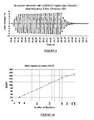
- the result, shown in FIG. 9 is a significant increase in efficiency compared to Figure 4 .
- the energy on the load is also increased by 50% compared to the case of Figure 4 , in spite of the charged energy being about 50% lower because of the high ratio of Z2/Z1.
- the chosen ratio of Z2/Z1 in this example is near the optimum for maximum energy delivered to the main load.
- the graph in Figure 10 represents a finding that illustrates the tendency of the optimum ratio of Z2/Z1 to increase with the number of sections in a generator where a 2-3 mil, low dielectric constant material is chosen for D1, and for high frequency pulses. All variations in the length of conductive segments and in impedances Z1 and/or Z2, as discussed for Figure 6 are applicable for Figures 7 , 8 and for followed Figure 11 .
- transmission line conductors 1105 and 1110 surround transmission line segments 1115 and 1120.
- the transmission lines are coupled to a main load 1125 and at the left side to a load 1130.
- the transmission line segments 1115 and 1120 are coupled to their corresponding transmission line at a distance D1 and have impedance Z1.
- the segments 1115 and 1120 are oppositely charged and pairs of switches at the same stage are activated together to create a double voltage pulse. It should be noted that the principle of increasing ratio of characteristic impedances of transmission lines without switches to characteristic impedances of transmission lines with switches may be applied to structures shown on Figures 13, 14, 15 in US-B-7 514 464 .
- the switch at transmission line segment #40 short circuited, operates as a series connected stub for all pulses generated by the preceding sections.
- the impedance of this transmission-line stub is 15 times lower compared to characteristic impedance of long transmission line with impedance Z1+Z2 (Z2 » Z1), in which generated pulses are traveling to the load 1125. This difference provides a much lower negative effect compared to the case where Z1 ⁇ Z2.
Landscapes
- Microwave Amplifiers (AREA)
- Waveguide Switches, Polarizers, And Phase Shifters (AREA)
Applications Claiming Priority (1)
| Application Number | Priority Date | Filing Date | Title |
|---|---|---|---|
| US12/216,490 US7986196B2 (en) | 2008-07-07 | 2008-07-07 | Method and apparatus for digital synthesis of long multi-cycle microwave pulses |
Publications (2)
| Publication Number | Publication Date |
|---|---|
| EP2144371A2 true EP2144371A2 (de) | 2010-01-13 |
| EP2144371A3 EP2144371A3 (de) | 2015-05-20 |
Family
ID=41226358
Family Applications (1)
| Application Number | Title | Priority Date | Filing Date |
|---|---|---|---|
| EP20090275051 Withdrawn EP2144371A3 (de) | 2008-07-07 | 2009-07-03 | Verfahren und Vorrichtung zur digitalen Synthese langer Multizyklus-Mikrowellenimpulse |
Country Status (2)
| Country | Link |
|---|---|
| US (2) | US7986196B2 (de) |
| EP (1) | EP2144371A3 (de) |
Families Citing this family (5)
| Publication number | Priority date | Publication date | Assignee | Title |
|---|---|---|---|---|
| US7633182B2 (en) * | 2005-11-09 | 2009-12-15 | Bae Systems Advanced Technologies, Inc. | Bipolar pulse generators with voltage multiplication |
| US7902695B2 (en) * | 2009-03-13 | 2011-03-08 | Bae Systems Information And Electronic Systems Integration Inc. | Bipolar pulse generators with voltage multiplication and pulse separation |
| US8744004B2 (en) * | 2010-03-26 | 2014-06-03 | Bae Systems Information And Electronic Systems Integration Inc. | High power pulse generator |
| US9306371B2 (en) * | 2011-07-18 | 2016-04-05 | Bae Systems Information And Electronic Systems Intergration Inc. | Frequency agile high power microwave generator |
| US9935218B2 (en) * | 2015-01-02 | 2018-04-03 | BAE Systems Information and Electronic Systems Integreation Inc. | Generation of flexible high power pulsed waveforms |
Citations (8)
| Publication number | Priority date | Publication date | Assignee | Title |
|---|---|---|---|---|
| GB589127A (en) | 1941-10-10 | 1947-06-12 | Alan Dower Blumlein | Improvements in or relating to apparatus for generating electrical impulses |
| US4176295A (en) | 1978-06-15 | 1979-11-27 | Westinghouse Electric Corp. | High peak power microwave generator using light activated switches |
| US4329686A (en) | 1980-06-18 | 1982-05-11 | The University Of Rochester | Methods and apparatus for generating microwave pulses and for the measurement and control thereof |
| US5109203A (en) | 1986-04-24 | 1992-04-28 | Energy Compression Research Corp. | Generated and method for generating microwaves |
| US5185586A (en) | 1986-04-24 | 1993-02-09 | Energy Compression Research Corp. | Method and apparatus for digital synthesis of microwaves |
| US7268641B2 (en) | 2005-06-08 | 2007-09-11 | Bae Systems Information And Electronic Systems Integration, Inc. | Method and apparatus for digital synthesis of microwaves |
| US7514464B2 (en) | 2003-12-18 | 2009-04-07 | Pfizer Limited | Substituted arylpyrazoles |
| US7518464B2 (en) | 2005-06-08 | 2009-04-14 | Bae Systems Information And Electronic Systems Integration Inc. | Method and apparatus for digital synthesis of microwaves through balanced transmission line structures |
Family Cites Families (3)
| Publication number | Priority date | Publication date | Assignee | Title |
|---|---|---|---|---|
| US5153442A (en) * | 1989-06-12 | 1992-10-06 | The United States Of America As Represented By The Secretary Of The Army | High power, solid state RF pulse generators |
| AU729396B2 (en) * | 1996-04-04 | 2001-02-01 | Mitsubishi Heavy Industries, Ltd. | Apparatus and method for treating exhaust gas and pulse generator used therefor |
| US7633182B2 (en) * | 2005-11-09 | 2009-12-15 | Bae Systems Advanced Technologies, Inc. | Bipolar pulse generators with voltage multiplication |
-
2008
- 2008-07-07 US US12/216,490 patent/US7986196B2/en not_active Expired - Fee Related
-
2009
- 2009-07-03 EP EP20090275051 patent/EP2144371A3/de not_active Withdrawn
-
2011
- 2011-06-14 US US13/159,680 patent/US8373518B2/en not_active Expired - Fee Related
Patent Citations (8)
| Publication number | Priority date | Publication date | Assignee | Title |
|---|---|---|---|---|
| GB589127A (en) | 1941-10-10 | 1947-06-12 | Alan Dower Blumlein | Improvements in or relating to apparatus for generating electrical impulses |
| US4176295A (en) | 1978-06-15 | 1979-11-27 | Westinghouse Electric Corp. | High peak power microwave generator using light activated switches |
| US4329686A (en) | 1980-06-18 | 1982-05-11 | The University Of Rochester | Methods and apparatus for generating microwave pulses and for the measurement and control thereof |
| US5109203A (en) | 1986-04-24 | 1992-04-28 | Energy Compression Research Corp. | Generated and method for generating microwaves |
| US5185586A (en) | 1986-04-24 | 1993-02-09 | Energy Compression Research Corp. | Method and apparatus for digital synthesis of microwaves |
| US7514464B2 (en) | 2003-12-18 | 2009-04-07 | Pfizer Limited | Substituted arylpyrazoles |
| US7268641B2 (en) | 2005-06-08 | 2007-09-11 | Bae Systems Information And Electronic Systems Integration, Inc. | Method and apparatus for digital synthesis of microwaves |
| US7518464B2 (en) | 2005-06-08 | 2009-04-14 | Bae Systems Information And Electronic Systems Integration Inc. | Method and apparatus for digital synthesis of microwaves through balanced transmission line structures |
Non-Patent Citations (3)
| Title |
|---|
| "Picosecond Microwave Pulse Generation", APPL. PHYS. LETTERS, vol. 38, no. 6, 1981 |
| PROUD ET AL.: "High Frequency Waveform Generation Using Optoelectronic Switching in Silicon", IEEE TRANS ON MICROWAVE THEORY AND TECHNIQUES, vol. MTT-26, no. 3, 1978 |
| ZUCKER: "Light Activated Semiconductor Switches", UCRL PREPRINT, October 1977 (1977-10-01) |
Also Published As
| Publication number | Publication date |
|---|---|
| US20100001807A1 (en) | 2010-01-07 |
| US8373518B2 (en) | 2013-02-12 |
| US20110254607A1 (en) | 2011-10-20 |
| US7986196B2 (en) | 2011-07-26 |
| EP2144371A3 (de) | 2015-05-20 |
Similar Documents
| Publication | Publication Date | Title |
|---|---|---|
| US7365615B2 (en) | Method and apparatus for digital synthesis of microwaves | |
| US7692509B2 (en) | Method and apparatus for digital synthesis of microwaves through balanced transmission line structures | |
| US8373518B2 (en) | Method and apparatus for digital synthesis of long multi-cycle microwave pulses | |
| EP2099131A2 (de) | Auf Transmissionslinien basierender Hochspannungsimpulsgenerator | |
| US4888556A (en) | Linear induction accelerator and pulse forming networks therefor | |
| US8232682B2 (en) | High power bipolar pulse generators | |
| EP2800273B1 (de) | Vorrichtung und verfahren zur verwendung bei der steuerung einer impulsabgabe | |
| CN106941346B (zh) | 基于PCBBlumlein传输线和PCB传输线变压器的模块化固态纳秒脉冲发生器 | |
| US5185586A (en) | Method and apparatus for digital synthesis of microwaves | |
| US9196817B2 (en) | High voltage switches having one or more floating conductor layers | |
| US5109203A (en) | Generated and method for generating microwaves | |
| US5153442A (en) | High power, solid state RF pulse generators | |
| US11218182B2 (en) | Systems and methods for generating radio frequency signals | |
| US8207634B2 (en) | Compact multi-cycle high power microwave generator | |
| CN111900955B (zh) | 一种多路高压脉冲同步触发系统及方法 | |
| CN115037282B (zh) | 一种纳秒高压脉冲驱动晶闸管过流导通装置和方法 | |
| RU2117386C1 (ru) | Генератор высоковольтных импульсов | |
| USH843H (en) | High power RF generation with optically activated bulk GaAs devices | |
| Nunnally et al. | A Basic UWB Transmitter Design and Experiments: Blumlein Impulse Generator and Tem Radiator | |
| Baum | Compact Electric Antennas | |
| Kim et al. | High-power/high-pulse repetition frequency (PRF) pulse generation using a laser-diode-activated photoconductive GaAs switch |
Legal Events
| Date | Code | Title | Description |
|---|---|---|---|
| PUAI | Public reference made under article 153(3) epc to a published international application that has entered the european phase |
Free format text: ORIGINAL CODE: 0009012 |
|
| AK | Designated contracting states |
Kind code of ref document: A2 Designated state(s): AT BE BG CH CY CZ DE DK EE ES FI FR GB GR HR HU IE IS IT LI LT LU LV MC MK MT NL NO PL PT RO SE SI SK SM TR |
|
| PUAL | Search report despatched |
Free format text: ORIGINAL CODE: 0009013 |
|
| AK | Designated contracting states |
Kind code of ref document: A3 Designated state(s): AT BE BG CH CY CZ DE DK EE ES FI FR GB GR HR HU IE IS IT LI LT LU LV MC MK MT NL NO PL PT RO SE SI SK SM TR |
|
| AX | Request for extension of the european patent |
Extension state: AL BA RS |
|
| RIC1 | Information provided on ipc code assigned before grant |
Ipc: H03K 3/86 20060101AFI20150410BHEP Ipc: H03K 3/53 20060101ALI20150410BHEP |
|
| 17P | Request for examination filed |
Effective date: 20151112 |
|
| RBV | Designated contracting states (corrected) |
Designated state(s): AT BE BG CH CY CZ DE DK EE ES FI FR GB GR HR HU IE IS IT LI LT LU LV MC MK MT NL NO PL PT RO SE SI SK SM TR |
|
| STAA | Information on the status of an ep patent application or granted ep patent |
Free format text: STATUS: THE APPLICATION IS DEEMED TO BE WITHDRAWN |
|
| 18D | Application deemed to be withdrawn |
Effective date: 20170201 |