EP2144375A2 - Récepteur haute fréquence et dispositif haute fréquence l'utilisant - Google Patents
Récepteur haute fréquence et dispositif haute fréquence l'utilisant Download PDFInfo
- Publication number
- EP2144375A2 EP2144375A2 EP09163963A EP09163963A EP2144375A2 EP 2144375 A2 EP2144375 A2 EP 2144375A2 EP 09163963 A EP09163963 A EP 09163963A EP 09163963 A EP09163963 A EP 09163963A EP 2144375 A2 EP2144375 A2 EP 2144375A2
- Authority
- EP
- European Patent Office
- Prior art keywords
- signal
- noise
- high frequency
- receiving
- pick
- Prior art date
- Legal status (The legal status is an assumption and is not a legal conclusion. Google has not performed a legal analysis and makes no representation as to the accuracy of the status listed.)
- Withdrawn
Links
Images



Classifications
-
- H—ELECTRICITY
- H04—ELECTRIC COMMUNICATION TECHNIQUE
- H04B—TRANSMISSION
- H04B15/00—Suppression or limitation of noise or interference
- H04B15/02—Reducing interference from electric apparatus by means located at or near the interfering apparatus
- H04B15/04—Reducing interference from electric apparatus by means located at or near the interfering apparatus the interference being caused by substantially sinusoidal oscillations, e.g. in a receiver or in a tape-recorder
-
- H—ELECTRICITY
- H04—ELECTRIC COMMUNICATION TECHNIQUE
- H04B—TRANSMISSION
- H04B1/00—Details of transmission systems, not covered by a single one of groups H04B3/00 - H04B13/00; Details of transmission systems not characterised by the medium used for transmission
- H04B1/38—Transceivers, i.e. devices in which transmitter and receiver form a structural unit and in which at least one part is used for functions of transmitting and receiving
- H04B1/40—Circuits
- H04B1/50—Circuits using different frequencies for the two directions of communication
- H04B1/52—Hybrid arrangements, i.e. arrangements for transition from single-path two-direction transmission to single-direction transmission on each of two paths or vice versa
- H04B1/525—Hybrid arrangements, i.e. arrangements for transition from single-path two-direction transmission to single-direction transmission on each of two paths or vice versa with means for reducing leakage of transmitter signal into the receiver
Definitions
- the present invention relates to a high frequency device using a high frequency receiver which enables images to be displayed on a display portion based on a signal from a digital signal processor.
- the high frequency device can be a portable phone, a portable game, a portable computer, a portable dictionary, a car navigation system, or the like.
- high frequency devices function as portable phones, portable games, portable computers, portable dictionaries, car navigation systems, and even portable TVs.
- a display portion In such a conventional high frequency device, a display portion, a system controller, and other components radiate a clock signal and a noise signal, which is a harmonic of the clock signal. These signals come into a TV antenna, causing degradation of reception quality, particularly in a weak electric field.
- the noise signals which have come into the TV antenna from the plurality of noise signal sources are cancelled using a plurality of noise cancellers.
- the noise signals from the noise signal sources differently affect the degradation of TV reception quality depending on the use conditions of the phone.
- the use conditions include: receiving a TV signal, recording TV program while the phone is in use, and recording TV program while the camera is in use.
- noise signals are cancelled using the same number of noise cancellers as the noise signal sources in consideration of various TV reception conditions. This requires a long processing time.
- the high frequency receiver of the present invention cancels a plurality of noise signals which are contained in a high frequency signal and outputted from a plurality of noise signal sources.
- the high frequency receiver cancels the noise signals by selecting at least one of a plurality of pick-up noise signals extracted from a plurality of pick-up antennas disposed near the noise signal sources.
- the high frequency receiver further includes on-off switches, which are turned on in descending order of the effects of the pick-up noise signals on the degradation of reception quality so as to implement noise cancelling.
- noise cancelling can be completed in a short time, thereby improving the reception quality of the high-frequency signal.
- High frequency device 101 can receive a UHF digital broadcast signal as a high-frequency signal, and has a phone function.
- High frequency device 101 includes high frequency receiver 103, transceiver 107, digital signal processor 109, and system controller 111.
- High frequency receiver 103 includes input terminal 103a connected to TV antenna 102.
- Transceiver 107 includes input-output terminal 107a connected to mobile phone antenna 105.
- Digital signal processor 109 is connected to the output signal of high frequency receiver 103 and to the input and output signals of transceiver 107.
- System controller 111 controls high frequency receiver 103, transceiver 107, and digital signal processor 109.
- High frequency device 101 further includes video display portion 115, audio output portion 117, and audio input portion 119, which are connected to digital signal processor 109.
- High frequency receiver 103 includes matching box 121, noise canceller 123, tuner 125, and demodulator circuit 127, which are connected in this order between input terminal 103a and output terminal 103b.
- Matching box 121 reduces the matching loss between TV antenna 102 and high frequency receiver 103.
- Noise canceller 123 cancels noise signals.
- Tuner 125 receives TV signals.
- Demodulator circuit 127 demodulates an input signal and outputs a TS (transport stream) signal.
- High frequency receiver 103 further includes receiving-signal-quality determining circuit 129, which determines the reception quality by comparing a BER (bit error rate) or a C/N (carrier-to-noise ratio) outputted from demodulator circuit 127 with a predetermined reference value.
- Receiving-signal-quality detecting circuit 129 supplies its determination signal to system controller 111 so as to control the entire system and to effect the start of the noise cancelling operation by noise canceller 123.
- Noise canceller 123 includes compositor 131 and cancel signal generating circuits 133, 137, and 138.
- Compositor 131 is connected between the output of matching box 121 and the input of tuner 125.
- Cancel signal generating circuit 133 is connected between input 131a of compositor 131 and input terminal 123a of noise canceller 123.
- Cancel signal generating circuit 137 is connected between input 131b of compositor 131 and input terminal 123b of noise canceller 123.
- Cancel signal generating circuit 138 is connected between input 131c of compositor 131 and input terminal 123c of noise canceller 123.
- Cancel signal generating circuit 133 includes phase controller 133a and gain controller 133b connected in series between its input and output.
- Cancel signal generating circuit 137 includes phase controller 137a and gain controller 137b connected in series between its input and output.
- Cancel signal generating circuit 138 includes phase controller 138a and gain controller 138b connected in series between its input and output.
- High frequency receiver 103 further includes input terminals 103c, 103d, and 103e connected to pick-up antennas 142a, 142b, and 142c, respectively.
- Input terminals 103c, 103d, and 103e are also referred to as input units 103c, 103d, and 103e, respectively.
- switches 139, 140, and 141 can be controlled either exclusively or in combination.
- Transceiver 107 includes transmitter-receiver circuit 144, modulator-demodulator circuit 143, power supply circuit 145, and pick-up antenna 142a.
- Transmitter-receiver circuit 144 is connected to input-output terminal 107a so as to process transmitted and received phone signals.
- Modulator-demodulator circuit 143 is connected to the output of transmitter-receiver circuit 144 so as to process modulated and demodulated signals.
- Power supply circuit 145 supplies power to transmission power amplifier (PA) included in transmitter-receiver circuit 144.
- Pick-up antenna 142a is disposed near power supply circuit 145 so as to extract a pick-up noise signal.
- PA transmission power amplifier
- Pick-up antennas 142b and 142c for extracting pick-up noise signals are disposed near digital signal processor 109 and near video display portion 115, respectively.
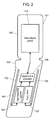
- Fig. 2 shows the arrangement of blocks, which are main components of high frequency device 101, where second case 165 is opened apart from first case 161 so that the user can talk or watch TV on the phone.
- first and second cases 161 and 165 are connected openably and closably by hinge part 163.
- second case 165 can be folded over first case 161 by hinge part 163 so as to be more compact and more portable.
- First case 161 includes TV antenna 102, high frequency receiver 103, mobile phone antenna 105, transceiver 107, and digital signal processor 109.
- Second case 165 includes video display portion 115 exposed on its side facing first case 161.
- high frequency device 101 thus structured will be described as follows with reference to Figs. 1 and 2 .
- An audio signal from audio input portion 119 is converted into a digital signal by digital signal processor 109, modulated by modulator-demodulator circuit 143, transmitted through transmitter-receiver circuit 144 and outputted from mobile phone antenna 105.
- a signal received by mobile phone antenna 105 is selected and frequency-converted by transmitter-receiver circuit 144, demodulated by modulator-demodulator circuit 143, converted into an analog signal by digital signal processor 109, and transmitted to video display portion 115 and audio output portion 117. This allows the user to view image or listen to audio.
- power supply circuit 145 supplying power to the transmission power amplifier (PA) of transmitter-receiver circuit 144, video display portion 115, and digital signal processor 109 radiate a clock signal and a UHF band noise signal, which is a harmonic of the clock signal. These signals come into TV antenna 102, causing degradation of reception quality, particularly in a weak electric field.
- PA transmission power amplifier
- noise canceller 123 The noise signals are reduced by noise canceller 123 as follows.
- Matching box 121 allows impedance matching between TV antenna 102 and high frequency receiver 103, ensuring receiving sensitivity even when TV antenna 102 is shorter.
- Matching box 121 outputs the TV signal and the high-frequency signal containing the noise signals came from the noise signal sources to noise canceller 123.
- cancel signal generating circuit 133 is used with switch 139 in the ON position. This makes it possible to cancel the noise signal which has come into TV antenna 102 from power supply circuit 145 for supplying power to the transmission power amplifier (PA) using a pick-up noise signal extracted from pick-up antenna 142a.
- PA transmission power amplifier
- cancel signal generating circuit 137 is used with switch 140 in the ON position. This makes it possible to cancel the noise signal which has come into TV antenna 102 from digital signal processor 109 using a pick-up noise signal extracted from pick-up antenna 142b.
- cancel signal generating circuit 138 is used with switch 141 in the ON position. This makes it possible to cancel the noise signal which has come into TV antenna 102 from video display portion 115 using a pick-up noise signal extracted from pick-up antenna 142c.
- At least one of the pick-up noise signals is selected and at least one of the noise signals can be cancelled.
- Noise canceller 123 outputs a high-frequency signal to tuner 125.
- tuner 125 a reception channel is selected and an intermediate frequency signal or a baseband signal is gain-controlled and frequency-converted at the direction of system controller 111.
- Tuner 125 outputs the frequency-converted signal to demodulator circuit 127.
- Demodulator circuit 127 demodulates the frequency-converted signal into a TS signal and outputs the TS signal through output terminal 103b to digital signal processor 109.
- Digital signal processor 109 outputs a video signal and an audio signal to video display portion 115 and audio output portion 117, respectively. This allows the user to view image or listen to audio.
- Demodulator circuit 127 also outputs a reception quality signal such as a BER or a C/N to receiving-signal-quality determining circuit 129, which determines the reception quality by comparing the BER or the C/N with the predetermined reference value.
- a reception quality signal such as a BER or a C/N
- receiving-signal-quality determining circuit 129 which determines the reception quality by comparing the BER or the C/N with the predetermined reference value.
- receiving-signal-quality determining circuit 129 may use an AGC (automatic gain control) voltage for gain-controlling an amplifier disposed in tuner 125.
- AGC automatic gain control
- the effects of noise signals from noise signal sources on TV reception quality are a problem for the receiving sensitivity in a weak electric field.
- the level of the weak electric field signal can be determined using the AGC voltage of the amplifier arranged at a later stage of tuner 125. In addition, the determination can be made quickly because the AGC voltage has a high response speed.
- Receiving-signal-quality determining circuit 129 outputs a determination signal to system controller 111, which optimizes the phase and the gain of phase controller 133a and gain controller 133b of cancel signal generating circuit 133.
- System controller 111 further optimizes the phase and the gain of phase controller 137a and gain controller 137b of cancel signal generating circuit 137, and also the phase and the gain of phase controller 138a and gain controller 138b of cancel signal generating circuit 138.
- noise canceller 123 receives the noise signals from the noise signal sources and the noise signals from the noise signal sources.
- receiving-signal-quality determining circuit 129 receives the noise signals from the noise signal sources.
- noise signals from the noise signal sources differently affect the degradation of TV reception quality depending on the operating conditions of high frequency device 101.
- Table 1 below shows the effects of the noise signals from the noise signal sources on the degradation of TV reception quality, depending on the operating conditions of high frequency device 101 when receiving a TV signal.
- Table 1 Operating conditions of high frequency device 101 when receiving a TV signal Portable phone Opened or Closed Power supply circuit 145 Digital signal processor 109 Video display portion 115 Pick-up antenna 142a Pick-up antenna 142b Pick-up antenna 142c Switch 139 Switch 140 Switch 141 1 standby mode opened, receiving a TV signal ⁇ ⁇ 2 standby mode closed, recording TV program ⁇ 3 standby mode, camera in use opened, recording TV program ⁇ ⁇ 4 in use opened, recording TV program ⁇ ⁇ ⁇
- Noise signal source has:
- the operating conditions of high frequency device 101 when receiving a TV signal include: receiving a TV signal, recording TV program while the phone is in use, and recording TV program while the camera is in use.
- a TV signal is received with second case 165 open when the phone is in the standby mode.
- noise signals come into TV antenna 102 from video display portion 115 and digital signal processor 109, and enter noise canceller 123.
- TV program recording is performed with second case 165 closed when the phone is in the standby mode.
- a noise signal comes into TV antenna 102 from digital signal processor 109 and enters noise canceller 123.
- an operating condition 3 to receive a TV signal camera portion 113 is operated and at the same time, TV program recording is performed with second case 165 open when the phone is in the standby mode.
- noise signals come into TV antenna 102 from video display portion 115 and digital signal processor 109 and enter noise canceller 123.
- TV program recording is performed while the phone is in use with second case 165 open.
- Noise signals come into TV antenna 102 from power supply circuit 145, video display portion 115, and digital signal processor 109, and enter noise canceller 123.
- the noise signal from power supply circuit 145 is larger than other the noise signals because the signal outputted from transceiver 107 requires a large signal level.
- the noise signal from digital signal processor 109 always have effects on the degradation of TV reception quality.
- digital signal processor 109 provides a higher clock frequency than the other noise signal sources.
- the noise signal from video display portion 115 has some effects on the degradation of TV reception quality because video display portion 115 is displayed open.
- the noise signal from video display portion 115 has some effects on the degradation of TV reception quality.
- the noise signal from power supply circuit 145 has the largest effects because the phone is in use.
- the noise signals from the noise signal sources differently affect the degradation of TV reception quality depending on the operating conditions of high frequency device 101 when receiving a TV signal.
- Fig. 3 is a flowchart of a noise cancelling operation.
- Step 231 a desired channel is selected using tuner 125.
- Step 231 is followed by Step 233.
- receiving-signal-quality determining circuit 129 determines the BER or the C/N based on the predetermined reference value. When it is determined to be good (OK), the determination of the BER is repeated through a return loop.
- Fig. 4A shows an output signal from tuner 125 in this case, where there are few noise signals from the noise signal sources.
- Received signal 255a has a bandwidth 259 of 5.6 MHz, and a center frequency 260 of 4 MHz.
- Noise signal 257 which is a base noise, is the sum of thermal noise power related to Boltzmann constant and the noise figure (NF) of high frequency device 101.
- Step 233 receiving-signal-quality determining circuit 129 determines the BER or the C/N based on the predetermined reference value.
- NG bad
- the process goes to Step 234 where a parameter P is initialized to "0".
- Fig. 4B shows an output signal from tuner 125 when received signal 255b is reduced in a weak electric field.
- Received signal 255b has a C/N reduced by noise signals 262 from the noise signal sources.
- Noise signals 262 are composed of noise signal 262a from power supply circuit 145, which supplies power to transmission power amplifier (PA), noise signal 262b from digital signal processor 109, and noise signal 262c from video display portion 115.
- Noise signal 262a is the largest, noise signal 262b is the second largest, and noise signal 262c is the smallest.
- Step 234 is followed by Step 235 in which the parameter P is set to "P + 1". Step 235 is then followed by Step 237.
- Step 237 switch 139 is turned on to make pick-up antenna 142a extract a pick-up noise signal.
- This allows the noise signal from power supply circuit 145 provided for the transmission power amplifier to be selected based on Table 1 showing the operating conditions to receive a TV signal.
- the noise signal from power supply circuit 145 has the largest effects on the degradation of TV reception quality.
- Step 237 is followed by Step 239.
- Step 239 cancel signal generating circuit 133 and compositor 131 cancel the noise signal which has come through input terminal 103a from power supply circuit 145. Step 239 is followed by Step 241.
- receiving-signal-quality determining circuit 129 determines whether a best value is obtained or not by comparing the current BER or C/N with the previous BER or C/N. The comparison is repeated by returning to Step 239 until the best value is obtained.
- Step 241 When the best value has been obtained in Step 241, the process goes to Step 243 in which the phase and gain of cancel signal generating circuit 133 obtained in Step 239 are maintained. Step 243 is followed by Step 245.
- Step 245 receiving-signal-quality determining circuit 129 determines the BER or the C/N based on the predetermined reference value.
- the process goes back to Step 233.
- the process goes back to Step 235 in which the parameter P is set to "2". Step 235 is followed by Step 237.
- Step 237 switch 140 is turned on with switch 139 in the ON position based on Table 1.
- Switch 139 is turned on to select the noise signal coming from power supply circuit 145, which has the largest effects on the degradation of TV reception quality.
- Switch 140 is turned on to select the noise signal coming from digital signal processor 109, which has the second largest effects on the degradation of TV reception quality.
- Step 237 is followed by Step 239 in which newly-added cancel signal generating circuit 137 and compositor 131 cancel the noise signal which has come through input terminal 103a from power supply circuit 145.
- Step 239 is followed by Step 241.
- receiving-signal-quality determining circuit 129 determines whether a best value is obtained or not by comparing the current BER or C/N with the previous BER or C/N. The comparison is repeated by returning to Step 239 until the best value is obtained.
- Step 241 When the best value has been obtained in Step 241, the process goes to Step 243 in which the phases and gains of cancel signal generating circuits 133 and 137 obtained in Step 239 are maintained. Step 243 is followed by Step 245.
- Step 245 receiving-signal-quality determining circuit 129 determines the BER or the C/N based on the predetermined reference value.
- the process goes back to Step 233.
- the process goes back to Step 235 in which the parameter P is set to "3". Step 235 is followed by Step 237.
- Step 237 switch 141 is turned on with switches 139 and 140 in the ON position based on Table 1 showing the operating conditions to receive a TV signal.
- Switch 141 is turned on to select the noise signal coming from video display portion 115, which has the smallest effects on the degradation of TV reception quality.
- Cancel signal generating circuit 138 cancels the noise signal using the pick-up noise signal picked up by pick-up antenna 142c.
- Step 237 the process goes to Steps 239 and 241, and when the best value is obtained, further goes to Steps 243 and 245.
- Steps 235 through 245 are repeated to reduce noise signals 262 close to noise signal 257, which is the base noise, thereby improving the C/N of the received signal.
- switches 139, 140, and 141 are turned on in this order. Therefore, the number P of switches is three.
- switches 140 and 141 are turned on in this order, and the number P of switches is two.
- the pick-up noise signals extracted from pick-up antennas 142a, 142b, and 142c are selected in descending order of their effects on the degradation of reception quality to perform noise cancelling until the reception quality is determined OK.
- the order in which to turn on the switches can be predetermined according to the operating conditions 1 to 4 to receive a TV signal, thereby completing noise cancelling in a shorter time.
- the noise signal from digital signal processor 109 always has effects on the degradation of TV reception quality. Therefore, it is possible to preferentially select switch 140 connected to pick-up antenna 142b, which picks up the noise signal from digital signal processor 109. Alternatively, it is possible to keep switch 140 in the ON state.
- a TV signal is a digital signal in the embodiment; however, the present invention is also applicable to receiving one segment signal or an analog signal.
Landscapes
- Engineering & Computer Science (AREA)
- Computer Networks & Wireless Communication (AREA)
- Signal Processing (AREA)
- Noise Elimination (AREA)
Applications Claiming Priority (2)
| Application Number | Priority Date | Filing Date | Title |
|---|---|---|---|
| JP2008178818A JP2010021683A (ja) | 2008-07-09 | 2008-07-09 | 高周波受信部とこれを用いた高周波機器 |
| JP2008178817A JP2010021682A (ja) | 2008-07-09 | 2008-07-09 | 高周波受信部とこれを用いた高周波機器 |
Publications (1)
| Publication Number | Publication Date |
|---|---|
| EP2144375A2 true EP2144375A2 (fr) | 2010-01-13 |
Family
ID=41176119
Family Applications (1)
| Application Number | Title | Priority Date | Filing Date |
|---|---|---|---|
| EP09163963A Withdrawn EP2144375A2 (fr) | 2008-07-09 | 2009-06-29 | Récepteur haute fréquence et dispositif haute fréquence l'utilisant |
Country Status (2)
| Country | Link |
|---|---|
| US (1) | US20100007742A1 (fr) |
| EP (1) | EP2144375A2 (fr) |
Cited By (1)
| Publication number | Priority date | Publication date | Assignee | Title |
|---|---|---|---|---|
| EP3020127A1 (fr) * | 2013-07-11 | 2016-05-18 | Qualcomm Incorporated | Alimentation à découpage à l'aide d'une commande de bruit |
Families Citing this family (6)
| Publication number | Priority date | Publication date | Assignee | Title |
|---|---|---|---|---|
| EP1879377A3 (fr) * | 2006-07-13 | 2010-06-16 | Panasonic Corporation | Dispositif portable |
| JP2011010262A (ja) * | 2009-05-28 | 2011-01-13 | Panasonic Corp | 携帯機器 |
| WO2012086566A1 (fr) | 2010-12-22 | 2012-06-28 | シャープ株式会社 | Dispositif de communication sans fil |
| US11057838B2 (en) * | 2011-12-09 | 2021-07-06 | Telefonaktiebolaget Lm Ericsson (Publ) | Adapting output power of a radio transmitting entity |
| US10382823B2 (en) * | 2016-03-28 | 2019-08-13 | Oath Inc. | Video content deep diving |
| CN115457747B (zh) * | 2022-10-21 | 2024-02-27 | 贵州广播电视台 | 一种信号异态的报警方法、装置、设备以及存储介质 |
Citations (1)
| Publication number | Priority date | Publication date | Assignee | Title |
|---|---|---|---|---|
| JP2008022294A (ja) | 2006-07-13 | 2008-01-31 | Matsushita Electric Ind Co Ltd | 携帯機器 |
Family Cites Families (5)
| Publication number | Priority date | Publication date | Assignee | Title |
|---|---|---|---|---|
| KR100351823B1 (ko) * | 2000-04-27 | 2002-09-11 | 엘지전자주식회사 | 사용자 오에스디(osd) 제공 장치 및 방법 |
| JP4417593B2 (ja) * | 2001-08-10 | 2010-02-17 | パイオニア株式会社 | アンテナ切替装置 |
| US6968171B2 (en) * | 2002-06-04 | 2005-11-22 | Sierra Wireless, Inc. | Adaptive noise reduction system for a wireless receiver |
| US20040042569A1 (en) * | 2002-09-03 | 2004-03-04 | Electro-Radiation Incorporated | Method and apparatus to provide communication protection technology for satellite earth stations |
| KR100754647B1 (ko) * | 2002-09-17 | 2007-09-05 | 삼성전자주식회사 | 휴대단말기의 텔레비전 영상신호 표시장치 및 방법 |
-
2009
- 2009-06-17 US US12/486,223 patent/US20100007742A1/en not_active Abandoned
- 2009-06-29 EP EP09163963A patent/EP2144375A2/fr not_active Withdrawn
Patent Citations (1)
| Publication number | Priority date | Publication date | Assignee | Title |
|---|---|---|---|---|
| JP2008022294A (ja) | 2006-07-13 | 2008-01-31 | Matsushita Electric Ind Co Ltd | 携帯機器 |
Cited By (1)
| Publication number | Priority date | Publication date | Assignee | Title |
|---|---|---|---|---|
| EP3020127A1 (fr) * | 2013-07-11 | 2016-05-18 | Qualcomm Incorporated | Alimentation à découpage à l'aide d'une commande de bruit |
Also Published As
| Publication number | Publication date |
|---|---|
| US20100007742A1 (en) | 2010-01-14 |
Similar Documents
| Publication | Publication Date | Title |
|---|---|---|
| EP2144375A2 (fr) | Récepteur haute fréquence et dispositif haute fréquence l'utilisant | |
| CN100512247C (zh) | 高频信号接收装置及其制造方法 | |
| US8185071B2 (en) | Tuner module | |
| EP1826928A1 (fr) | Recepteur haute frequence, circuit integre utilise dans celui-ci, dispositif mobile les utilisant, transmetteur utilise dans celui-ci et leur procede de fabrication | |
| US8577428B2 (en) | Information processing apparatus | |
| US20100253851A1 (en) | Noise canceller and electronic device using the same | |
| JP2008259195A (ja) | 携帯通信端末機の干渉雑音除去装置及び方法 | |
| US20090195701A1 (en) | Noise canceller as well as high-frequency receiver and portable device each using the same | |
| JP4287855B2 (ja) | モバイルのテレビジョン受信機用集積回路 | |
| JP5161854B2 (ja) | 受信装置、受信装置のアンテナ切替え回路、及び受信装置のチューナモジュール | |
| JP4235560B2 (ja) | チューナ用の自動利得制御 | |
| US20050090207A1 (en) | Diversity reception tuner | |
| US20050253973A1 (en) | Mobile device | |
| JP2010021682A (ja) | 高周波受信部とこれを用いた高周波機器 | |
| US7672654B2 (en) | Broadcasting receiver and method of receiving a broadcasting wave | |
| KR20010006770A (ko) | 디지털 신호 수신 장치 및 방법, 및 제공 매체 | |
| US20040031064A1 (en) | Cable receiver having in-band and out-of-band tuners | |
| JP2009253314A (ja) | 高周波受信部とこれを用いた高周波機器 | |
| JP2005311536A (ja) | 無線装置 | |
| JP2010021683A (ja) | 高周波受信部とこれを用いた高周波機器 | |
| EP1710921A1 (fr) | Terminal mobile et procédé pour la réception de signaux de radiodiffusion | |
| US20070030062A1 (en) | Matching device for an antenna and high-frequency receiver using the same | |
| US20050143030A1 (en) | Receiving apparatus | |
| JP2008022294A (ja) | 携帯機器 | |
| JP2010193369A (ja) | 受信システムおよび受信方法 |
Legal Events
| Date | Code | Title | Description |
|---|---|---|---|
| PUAI | Public reference made under article 153(3) epc to a published international application that has entered the european phase |
Free format text: ORIGINAL CODE: 0009012 |
|
| AK | Designated contracting states |
Kind code of ref document: A2 Designated state(s): AT BE BG CH CY CZ DE DK EE ES FI FR GB GR HR HU IE IS IT LI LT LU LV MC MK MT NL NO PL PT RO SE SI SK TR |
|
| STAA | Information on the status of an ep patent application or granted ep patent |
Free format text: STATUS: THE APPLICATION HAS BEEN WITHDRAWN |
|
| 18W | Application withdrawn |
Effective date: 20110803 |