EP2145224B1 - Formation de faisceaux lumineux et motifs avec points centraux d'intensité zéro - Google Patents
Formation de faisceaux lumineux et motifs avec points centraux d'intensité zéro Download PDFInfo
- Publication number
- EP2145224B1 EP2145224B1 EP08729324.7A EP08729324A EP2145224B1 EP 2145224 B1 EP2145224 B1 EP 2145224B1 EP 08729324 A EP08729324 A EP 08729324A EP 2145224 B1 EP2145224 B1 EP 2145224B1
- Authority
- EP
- European Patent Office
- Prior art keywords
- plate
- wavelength
- axis
- plates
- portions
- Prior art date
- Legal status (The legal status is an assumption and is not a legal conclusion. Google has not performed a legal analysis and makes no representation as to the accuracy of the status listed.)
- Not-in-force
Links
- 238000000034 method Methods 0.000 claims description 19
- 239000000203 mixture Substances 0.000 claims description 16
- 238000009826 distribution Methods 0.000 claims description 12
- 239000012780 transparent material Substances 0.000 claims description 9
- 230000010363 phase shift Effects 0.000 claims description 8
- 230000001934 delay Effects 0.000 claims description 3
- 239000010410 layer Substances 0.000 claims 2
- 241000711981 Sais Species 0.000 claims 1
- 238000007493 shaping process Methods 0.000 claims 1
- 239000002356 single layer Substances 0.000 claims 1
- 239000011521 glass Substances 0.000 description 67
- 235000012489 doughnuts Nutrition 0.000 description 21
- 230000003287 optical effect Effects 0.000 description 12
- 238000010791 quenching Methods 0.000 description 12
- 230000005284 excitation Effects 0.000 description 11
- 230000000171 quenching effect Effects 0.000 description 11
- 230000003595 spectral effect Effects 0.000 description 8
- 230000008859 change Effects 0.000 description 5
- 238000003491 array Methods 0.000 description 4
- 238000012937 correction Methods 0.000 description 4
- 230000001902 propagating effect Effects 0.000 description 4
- 230000005855 radiation Effects 0.000 description 4
- 238000001228 spectrum Methods 0.000 description 4
- 238000013519 translation Methods 0.000 description 4
- RTAQQCXQSZGOHL-UHFFFAOYSA-N Titanium Chemical compound [Ti] RTAQQCXQSZGOHL-UHFFFAOYSA-N 0.000 description 3
- 230000006872 improvement Effects 0.000 description 3
- 238000004519 manufacturing process Methods 0.000 description 3
- 238000000386 microscopy Methods 0.000 description 3
- 210000001747 pupil Anatomy 0.000 description 3
- 230000000979 retarding effect Effects 0.000 description 3
- 229910052719 titanium Inorganic materials 0.000 description 3
- 239000010936 titanium Substances 0.000 description 3
- 238000010870 STED microscopy Methods 0.000 description 2
- 239000006117 anti-reflective coating Substances 0.000 description 2
- 230000008901 benefit Effects 0.000 description 2
- 230000015572 biosynthetic process Effects 0.000 description 2
- 230000007423 decrease Effects 0.000 description 2
- 230000003247 decreasing effect Effects 0.000 description 2
- 230000003111 delayed effect Effects 0.000 description 2
- 239000006185 dispersion Substances 0.000 description 2
- 239000000835 fiber Substances 0.000 description 2
- 239000011159 matrix material Substances 0.000 description 2
- 238000005498 polishing Methods 0.000 description 2
- 238000000926 separation method Methods 0.000 description 2
- 241000511976 Hoya Species 0.000 description 1
- 238000010521 absorption reaction Methods 0.000 description 1
- 230000001133 acceleration Effects 0.000 description 1
- 238000004026 adhesive bonding Methods 0.000 description 1
- 230000009286 beneficial effect Effects 0.000 description 1
- 230000005540 biological transmission Effects 0.000 description 1
- 229910052792 caesium Inorganic materials 0.000 description 1
- TVFDJXOCXUVLDH-UHFFFAOYSA-N caesium atom Chemical compound [Cs] TVFDJXOCXUVLDH-UHFFFAOYSA-N 0.000 description 1
- 238000000576 coating method Methods 0.000 description 1
- 238000013480 data collection Methods 0.000 description 1
- 238000013500 data storage Methods 0.000 description 1
- 230000002939 deleterious effect Effects 0.000 description 1
- 238000013461 design Methods 0.000 description 1
- 230000001627 detrimental effect Effects 0.000 description 1
- 238000010586 diagram Methods 0.000 description 1
- 239000012467 final product Substances 0.000 description 1
- 239000007850 fluorescent dye Substances 0.000 description 1
- 229910052734 helium Inorganic materials 0.000 description 1
- 239000001307 helium Substances 0.000 description 1
- SWQJXJOGLNCZEY-UHFFFAOYSA-N helium atom Chemical compound [He] SWQJXJOGLNCZEY-UHFFFAOYSA-N 0.000 description 1
- 238000003384 imaging method Methods 0.000 description 1
- 230000000873 masking effect Effects 0.000 description 1
- 238000005259 measurement Methods 0.000 description 1
- 230000007246 mechanism Effects 0.000 description 1
- QSHDDOUJBYECFT-UHFFFAOYSA-N mercury Chemical compound [Hg] QSHDDOUJBYECFT-UHFFFAOYSA-N 0.000 description 1
- 229910052753 mercury Inorganic materials 0.000 description 1
- 238000001393 microlithography Methods 0.000 description 1
- 239000013307 optical fiber Substances 0.000 description 1
- 238000012576 optical tweezer Methods 0.000 description 1
- 239000002245 particle Substances 0.000 description 1
- 102000004169 proteins and genes Human genes 0.000 description 1
- 108090000623 proteins and genes Proteins 0.000 description 1
- 238000004621 scanning probe microscopy Methods 0.000 description 1
Images


Classifications
-
- G—PHYSICS
- G01—MEASURING; TESTING
- G01N—INVESTIGATING OR ANALYSING MATERIALS BY DETERMINING THEIR CHEMICAL OR PHYSICAL PROPERTIES
- G01N21/00—Investigating or analysing materials by the use of optical means, i.e. using sub-millimetre waves, infrared, visible or ultraviolet light
- G01N21/62—Systems in which the material investigated is excited whereby it emits light or causes a change in wavelength of the incident light
- G01N21/63—Systems in which the material investigated is excited whereby it emits light or causes a change in wavelength of the incident light optically excited
- G01N21/64—Fluorescence; Phosphorescence
-
- G—PHYSICS
- G02—OPTICS
- G02B—OPTICAL ELEMENTS, SYSTEMS OR APPARATUS
- G02B27/00—Optical systems or apparatus not provided for by any of the groups G02B1/00 - G02B26/00, G02B30/00
- G02B27/09—Beam shaping, e.g. changing the cross-sectional area, not otherwise provided for
- G02B27/0938—Using specific optical elements
- G02B27/0988—Diaphragms, spatial filters, masks for removing or filtering a part of the beam
-
- G—PHYSICS
- G02—OPTICS
- G02B—OPTICAL ELEMENTS, SYSTEMS OR APPARATUS
- G02B27/00—Optical systems or apparatus not provided for by any of the groups G02B1/00 - G02B26/00, G02B30/00
- G02B27/09—Beam shaping, e.g. changing the cross-sectional area, not otherwise provided for
- G02B27/0927—Systems for changing the beam intensity distribution, e.g. Gaussian to top-hat
-
- G—PHYSICS
- G01—MEASURING; TESTING
- G01N—INVESTIGATING OR ANALYSING MATERIALS BY DETERMINING THEIR CHEMICAL OR PHYSICAL PROPERTIES
- G01N2201/00—Features of devices classified in G01N21/00
- G01N2201/06—Illumination; Optics
- G01N2201/061—Sources
- G01N2201/06113—Coherent sources; lasers
-
- G—PHYSICS
- G02—OPTICS
- G02B—OPTICAL ELEMENTS, SYSTEMS OR APPARATUS
- G02B21/00—Microscopes
- G02B21/0004—Microscopes specially adapted for specific applications
- G02B21/002—Scanning microscopes
- G02B21/0024—Confocal scanning microscopes (CSOMs) or confocal "macroscopes"; Accessories which are not restricted to use with CSOMs, e.g. sample holders
- G02B21/0032—Optical details of illumination, e.g. light-sources, pinholes, beam splitters, slits, fibers
-
- G—PHYSICS
- G03—PHOTOGRAPHY; CINEMATOGRAPHY; ANALOGOUS TECHNIQUES USING WAVES OTHER THAN OPTICAL WAVES; ELECTROGRAPHY; HOLOGRAPHY
- G03F—PHOTOMECHANICAL PRODUCTION OF TEXTURED OR PATTERNED SURFACES, e.g. FOR PRINTING, FOR PROCESSING OF SEMICONDUCTOR DEVICES; MATERIALS THEREFOR; ORIGINALS THEREFOR; APPARATUS SPECIALLY ADAPTED THEREFOR
- G03F7/00—Photomechanical, e.g. photolithographic, production of textured or patterned surfaces, e.g. printing surfaces; Materials therefor, e.g. comprising photoresists; Apparatus specially adapted therefor
- G03F7/70—Microphotolithographic exposure; Apparatus therefor
- G03F7/70058—Mask illumination systems
- G03F7/70191—Optical correction elements, filters or phase plates for controlling intensity, wavelength, polarisation, phase or the like
Definitions
- the present invention relates to optical devices, and more particularly, devices for modifying the profile of a propagating beam. Still more particularly the present invention relates to devices that create beams either having a substantially zero intensity on their propagation axis and/or that when focused have a substantially zero intensity at a central point in the plane of focus.
- the optimum wavelength of the quenching beam depends on the fluorescent dye or protein, it is desirable to have a method for forming such beams where the wavelength can be changed, sometimes very rapidly, while preserving the zero-intensity of the beam central point. Also, it is sometimes desirable to make such doughnut shaped beams with light of very short pulses that have a relatively broad spectral distribution. Finally, to improve the quality of the doughnut beam produced, it may be desirable to locate the doughnut beam making means as close as possible to the microscope objective lens as possible, in which case the fluorescent light emitted from the specimen would have to pass through said means in addition to both the excitation and quenching beams, and each of these bands of light would in general have different wavelengths. Therefore, ideally, the method for making the zero-centered doughnut-shaped beams would be invariant with respect to the wavelength.
- SLM Spatial Light Modulator
- This proposed solution involves introducing additional optics to direct the beam onto the SLM and pass the reflected beam to the rest of the system, and in some cases to expand the beam for presentation to the SLM and to contract it for presentation to the rest of the optical system, and such optics create an opportunity for scattering, spurious reflection and introduction of additional phase errors.
- the system is relatively expensive, and cannot deal with extremely rapid changes in wavelength required in some microscope techniques or creation of zero-center patterns from an intrinsically broadband source.
- Gugel U.S. Patent Appl 2006/0007535 A1
- Gugel has proposed using the relative wavelength independent phase shift during total internal reflection, combined with the difference in phase shift depending on whether or not there is a metallic backing layer overlying the reflecting surface, to approximate an achromatic phase shift, between a beam portion reflected from a surface with a metallic backing layer compared to a beam portion reflected from a surface without such a metallic backing layer.
- the absorption does show a wavelength dependence, so that it is difficult or impossible to ensure cancellation at the central point over a wide range of wavelengths.
- One object of the present invention is to provide a method of producing beams with an intensity distribution having a substantially zero intensity along the beam axis and/or in the beam focus, where the method allows the wavelength of the light to be changed without requiring any readjustment.
- Another object of the present invention is to provide a method of producing beams with an intensity distribution having a substantially zero intensity along the beam axis and/or in the focus, where the beam has a broad spectral distribution.
- Another object of the present invention is to provide a method of producing beams with an intensity distribution having a substantially zero intensity along the beam axis and/or in the focus which allows laser beams to be converted to such beam without requiring any beam expansion.
- Another object of the present invention is to provide a method of producing beams with an intensity distribution having a substantially zero intensity along the beam axis and/or in the focus that consists of just transparent elements with parallel surfaces.
- Another object of the present invention is to provide a device for producing beams with an intensity distribution having a substantially zero intensity along the beam axis and/or in the focus, that is sufficiently compact to be able to conveniently fit inside a microscope body, even, if necessary, close to the pupil plane of the objective lens.
- a search is made for pairs of glass types that, at a particular thickness for each glass in the pair, the phase difference in propagation of light through one glass of the pair is exactly one half a wavelength relative to the other glass of the pair, for at least three different wavelengths spread out in the wavelength region of difference.
- one glass of the pair is called A and has a thickness TA
- the other glass is B and has a thickness TB
- eight squares of glass are made, two squares "A" of glass A of thickness TA, two squares "A*" of glass A of thickness TA/2, two squares "B” of glass B of thickness TB and two squares "B*" of glass B of thickness TB/2.
- Fig. 1 shows an exemplary embodiment of the present invention, in which elements 1 through 8 are glass sheets arranged in a sandwich of two 2x2 matrices, oriented normal to a laser beam 9 shown in the drawing by just its central ray. The direction of light in beam 9 is shown by an arrow.
- Sheets 1 and 3 are made of Sumita K-PMK10 glass of 82.503 ⁇ m in thickness.
- Sheets 2 and 4 are made of Schott N-PK51 glass of 82.286 ⁇ m in thickness.
- Sheets 5 and 6 are made of Sumita K-PMK10 glass of 165.005 ⁇ m in thickness.
- Sheets 7 and 8 are made of Schott N- PK51 glass of 164.571 ⁇ m in thickness.
- Fig. 2 shows a graph of the error as a fraction of a wavelength, plotted against wavelength, for the deviation from half wavelength relative retardation for two beams, one passing through a sheet, such as sheets 5 and 6 of Sumita K-PMK10 glass of 165.005 ⁇ m thick and the other passing through a sheet, such as sheets 7 and 8 of Schott N- PK51 glass of 164.571 ⁇ m thick.
- the curve shows that, over a spectral range from about .68 to 1.1 ⁇ m, the wavelength difference in the light from two beams which enter the plates in phase, will emerge with phase difference which is equal to a lambda/2 (half wavelength), within an error of less than about lambda/2000.
- the laser beam 9 must pass through sheet 1 before passing through sheet 6, and must pass through sheet 3 before passing through sheet 8. Because sheets 1 and 3 are made of the same glass and have the same thickness, they will not contribute any phase difference to the light, so the phase difference is determined entirely by sheets 6 and 8, and therefore will correspond almost exactly to a half wavelength, over the spectral range from .68 to 1.1 ⁇ m. For the same reason, there is a half wavelength difference between the portion of beam 9 passing through sheets 5 and 7.
- the plate is corrected almost exactly over the full range of the Titanium: Sapphire laser commonly used to form doughnut beams in STED microscopes.
- the device shown in Fig. 1 is completely corrected at the three wavelengths where the phase error is exactly zero, and is therefore apochromatic.
- the thickness of the glass sheets has been specified to nanometer precision, there is some range where deviations from this specified thickness by one sheet could largely be compensated by a corresponding variation in the opposing sheet. This would permit a manufacturing operation, where sheets could be manufactured with, say, a 100 nm tolerance, but measured to a 1 nm tolerance, and matched to an appropriate opposing sheet.
- Fig. 3 illustrates an arrangement of the plates shown in Fig. 1 , where instead of being normal to the incident laser beam 9, the four-quadrant phase plate is tilted with respect to the beam. Because the tilting increases causes refraction at the plate surface, which increases the path length within the plate, it is necessary to decrease plate thickness to compensate for the tilting.
- the tilting of sheets 1, 2, 3 and 4 is on a common axis 10 and tilting of sheets 5, 6, 7 and 8 is on a common axis 11.
- One advantage with the tilting is that by tilting each individual member sheet within the array can individually adjust for deviations from the intended thickness. In the case of the arrangement in Fig. 1 , tilting can only add effective thickness, not remove it, while with the arrangement in Fig. 3 , tilting can both add and remove effective thickness.
- Hinges for tilting include leaf springs, knife edges and needle and cylindrical bearings. Adjustment of the angle could be with a screw, for example.
- sheets 5 and 6 of Fig. 3 have been combined to form one sheet 15 and sheet 7 and 8 have been combined to form one sheet 16. This is possible both because the combined sheets are the made of the same glass and have the same thickness. Any variations in thickness between the two halves of sheet 15, for example, could be compensated by the tilting of sheet 1, and any variations in thickness of the two halves of sheet 16 could be compensated by the tilting of sheet 2.
- the ability to separately adjust the tilt of the 6 sheets in the apparatus of Fig 4 allows full adjustment of the effective thickness of each sheet to optimum correction. And once adjusted, the adjustment will not have to be redone as the wavelength changes over the range of applicability, in this case from about .7 to 1.2 ⁇ m.
- the edges of the sheets that meet in the center are beveled to approximate vertical planes (more accurately, they are beveled to be parallel to the angle that a ray from beam 9 is refracted in the sheet). This allows the sheets to be closer to minimize the light from beam 9 passing between the sheets. Any residual light passing between the sheets is blocked by a cross shaped obstruction (unillustrated), since it would otherwise tend to increase the brightness of the central point of the doughnut-shaped pattern produced, which would have a deleterious effect in many applications.
- Fig. 5 shows the preferred embodiment of the present invention, in which a pyramid 20 is made of triangles of parallel-sided glass sheets, through which the laser beam 9 must traverse on its way to the sandwich of sheets.
- Pyramid 20 will refract four quadrants of beam 9 away from the axis, as shown by Fig. 6 , which is a cross section through the pyramid, showing how two of its triangular plates 25 and 26, separately refract the portion of the beam 9 passing through them away from the axis.
- This separation is potentially beneficial because it allows the beam to avoid the area where the plates such as sheet 15 and sheet 16 meet, which without the pyramid would require masking to prevent transmission of the laser beam through that meeting area.
- beam 9 has a Gaussian distribution, such separation may increase both the intensity and the sharpness of the doughnut produced.
- Fig. 7 shows a curve for the deviation from half-wavelength phase difference for a ray passing normally through a sheet of Schott SF11 glass of 391.9325 ⁇ m thickness and a sheet of Schott N-SF6 glass of 381.635 ⁇ m thickness. It can be seen that the phase error is slightly less at the long wavelength end of the range between .6 and 1.2 ⁇ m, but is slightly greater at values on the intermediate and shorter wavelength parts of that range.
- the particular strategy for this search was 1) placing the all the different glasses in the Schott, Sumita, Hoya and Ohara catalogs in order of refractive index of the 852 nm cesium line, 2) for each pair of glasses separated by 43 positions or less on this ordered list, using the published refractive index at the 706.5 nm helium line and the 1014 nm mercury lines, finding the thickness of glass plates which will cause exactly a half wavelength propagation delay difference at these two lines, 3) using the calculated thickness at these wavelengths, and the refractive index at the 852 nm line, computing the error from half wavelength at the 852 nm line, a low error suggesting that the curve crosses the zero error line at three wavelengths in the desired spectral range, 4) for those glass pairs which both had a low error at 852 nm and also glass thickness that appeared practical for implementation of the present invention, computing the refractive index at 10 nm intervals, over the range from 600 nm to 1200 nm using the Sellmeier equation with published coefficient
- the essential goal is to find glass pairs such that for each member of the pair, there is a thickness of a sheet, such that for three wavelengths spread out in a chosen wavelength range of application for the device, one generally near the blue end of the range, one generally close to the middle of the range, and the third generally close to the red end of the range, light passing normally through one of the sheets is delayed exactly a half wavelength with respect to light passing through the other sheet, and at all intermediate values the relative delay is close to a half-wavelength.
- the two-sheet sandwich of the device of Fig. 1 is replaced by a single sheet layer.
- This embodiment of the present invention would make assembly of the final product easier, and would eliminate two air/glass interfaces, per beam path for decreased spurious reflection, which should improve resolution.
- One way to implement the embodiment shown in Fig. 8 would be to laminate the sheet pairs, using various techniques known to make strong bonds between glass sheets without the use of any adhesive bonding layer, eg., described in Howlader et al, Sensors and Actuators A: Physical, 127:31(06 ).
- sheets 3 and 8 of Fig. 1 would be bonded together to form sheet 33 of Fig. 8
- sheets 2 and 7 of Fig. 1 would be bonded to form sheet 32 of Fig. 8 etc.
- FIG. 8 Another way to implement the embodiment shown in Fig. 8 would be to find two pairs of glass compositions, such that each pair can yield an achromatic half wavelength difference when used for diagonal sheets, but the wavelength difference between adjacent sheets is a quarter wave.
- One possible such four glass combination would use as one pair of diagonally opposite sheets, eg., sheets 31 and 33, the same glasses and thicknesses illustrated in Fig. 1 (i.e., Sumita K-PMK10 glass, 165.005 ⁇ m thick and Schott N-PK51 glass, 164.571 ⁇ m thick.)
- a suitable glass pair for the remaining diagonally opposite sheets 32 and 34 would be, would be Schott N-PSK3 glass, 156.742 ⁇ m thick and Sumita G-FK68 146.635 ⁇ m thick.
- This particular four glass combination has a slightly greater error than the device shown in Fig. 1 , but the error is low enough that it might not make any practical difference. And the convenience of having just one non-laminated plate per quadrant might
- One additional four-glass composition has as one opposite pair is N-SSK2, 259.23 ⁇ m thick and N-LAK10, 223.665 ⁇ m, and the other opposite pair is N-SK4, 263,352 ⁇ m thick and N-LAK9, 233.15 ⁇ m thick.
- the half-wavelength error from about .7 to 1.0 ⁇ m was less than about .005 wavelengths, while the adjacent pairs have a quarter-wavelength error between pairs of less than about .02 wavelengths over the same spectral range.
- Fig. 9 The utility of the present invention is illustrated particularly in the Single Wavelength STED microscope apparatus shown in Fig. 9 , which is an improvement of the devices disclosed in Baer, PCT US 06/01961 , the entire disclosure of which is incorporated herein by reference.
- All prior art STED microscopes having the capacity to create zero-center doughnut patterns have included means for converting an incoming laser beam, usually with a Gaussian profile, into a beam with a zero intensity axial ray, and/or a substantially zero-centered doughnut pattern in the focal plane of the specimen. Every optical element between such converting means and the objective lens of the microscope is a potential source of wavefront distortion, scattering and spurious reflections that can lower the quality of the imaged doughnut-shaped pattern.
- Laser beam 40 from a Titanium:Sapphire laser, consisting of a train of pulses of duration on the order of 100 fs, and a frequency on the order of 100 MHz, passes through a rotatable half-wave plate 41 on its way to polarizing beam splitter 42, which transmits the minor fraction of the beam power as beam 43. Beam 43 will ultimately become focused to form the excitation spot.
- Beam splitter 42 reflects a major fraction of the incoming beam power as beam 44, which will become the doughnut-shaped quenching beam, the precise division of power between beams 43 and 44 being determined by the rotation of half-wave plate 41.
- Beam 44 is focused by lens 45 onto one end 46 of a long optical fiber 47, which by introducing group-velocity dispersion, stretches the pulse to the order of 200 ps or longer.
- polarizing beam splitter 51 which reflects nearly 100% of beam 50 to the microscope body where it is reflected by dichroic beam splitter 53 through the scanner and intermediate optics in box 54, and then through a quarter-wave plate 55 to convert the plane polarized light to circularly polarized.
- This circularly polarized light in a collimated beam is then passed through the four-quadrant device 56 of the present invention, converting it to a zero intensity axis beam, which the objective 57 then focuses to a doughnut-shaped pattern at the focal plane of specimen 58.
- the scanning means such as galvanometer mirrors (unillustrated) within box 54 limit the angle with respect to the optical axis, to an angle small enough so as not to disturb the relative retardation of the sheets of device 56 will remain accurate
- scanning can be provided by such means, and the doughnut will be scanned in a raster pattern over the chosen focal area of specimen 58 by means of scanners in box 54.
- the highest amplitude scan would be possible in such case, when four quadrant plate 56 were of the type shown in Figs. 1 and 8 , where the surface of the sheets is normal to the optical axis, since with such orientation, small angle deviations from the normal will make a minimal change in path length through the sheets.
- scanning can be provided by lateral translation of the objective 57 and or the specimen 58, or possibly both, with translation of the objective producing high frequency line scanning and translation of the specimen producing the lower frequency frame scanning.
- Still another method of scanning would be to have a vibrating mirror scanner provide a very low amplitude line scan for a narrow strip, which is scanned in the orthogonal direction by a slower movement of the objective.
- a still slower movement of the specimen relative to the objective moves the area of the scanned strips over the desired field of the specimen.
- the angular movement of the beam relative to four-quadrant plate 56 can be held to within limits that do not affect its phase retardation calibration, and but at the same time, the movement of elements close to the specimen can be relatively slow.
- That portion of beam 40 which is transmitted by polarizing beam splitter 42 to form beam 43 is directed through a second four-quadrant plate 60 of the present invention, similar to four-quadrant plate 56, but where the phase change is in the opposite direction (as if plate 56 were turned upside down).
- Plate 60 may be in a plane conjugate to plate 56 (from imaging of plate 56 onto plate 60 by relay lens optics in box 54 and at other, unillustrated places in the ray paths), so that each of the sheets in plate 60 is imaged on a corresponding sheet in plate 56.
- any relative phase changes due plate 60 are, as best as possible, cancelled by passage through plate 56, so that beam 43 is focused to a spot in specimen 58, such that the central maximum point of the spot coincides with the zero point of the doughnut-shaped beam.
- passage through the two plates 60 and 56 may not exactly cancel the phase retardations, and as such the focused spot of excitation light may be of larger diameter than if plates 60 and 56 were not in the path.
- resolution is determined by the half-width of the central minimum of the doughnut shaped beam, such imperfections in the formation of the excitation spot will not affect resolution.
- the electrical signal from detector 61 by synchronization with the scanning movements of the excitation spot relative to the specimen, leads to the formation of an image, by means well known in the art of laser scanning microscopy.
- the wide spectral correction of the four quadrant plate 56 is particularly important in the device of Fig. 9 because not only does it have to be corrected at the wavelengths of the excitation and quenching beams, but it also must be corrected for the intrinsically broad band spectrum of the fluorescent emission. Furthermore the fact that the four quadrant plate of the present invention is compact and does not require any adjustment after its initial calibration leads itself to the device of Fig. 9 , where the three four-quadrant plates can be imbedded into the optical system, without requiring constant access.
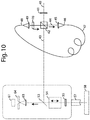
- a second example of Single Wavelength STED microscope in Fig. 10 where the design goal was to produce a STED microscope of maximum simplicity and minimum cost. All the elements that have the same function as in the microscope of Fig. 9 have been labeled as in Fig. 9 , and the function will not be described further here. It will be seen that the single polarizing beam splitter 42 functions both in its original role as shown in Fig. 9 , but also in the role of beam splitter 51 of Fig. 9 .
- the microscope of Fig. 10 contains just one four-quadrant plate 70 located between the recollimating lens 49 and beam splitter 42. Plate 70 may be in a pupil plane of the microscope. Because the axis of the light incident on plate 70 does not change with scanning, such scanning may be by rotating mirrors in box 54, and plate 70 need not be normal to the optical axis, facilitating adjustment of the thickness of its individual sheets.
- the components in the microscope of Fig. 10 already on a multiphoton microscope have been shown with dotted lines, to emphasize how few components have to be added to such a microscope to convert it into a STED microscope.
- the microscope of Fig. 10 is expected to produce a doughnut-shaped pattern that has more residual brightness of the central point than the pattern produced by the device of Fig. 9 , because additional optical elements intervene between the four-quadrant plate and the objective. However because the superior wavelength correction of the four-quadrant plate it is expected that the microscope would produce images that match or exceed those of any other state of the art STED microscope.
- the sheets be made of glass, however they could be made of other transparent materials.
- the examples in the description considered the beam passing through four quadrants, it is possible to imagine alternative embodiments of the invention with different numbers of sectors, where opposite sectors have a half wave phase difference, but where the phase difference between adjacent sectors decreases as the number of sectors increases.
- the examples given showed the application of the present invention to STED microscopy, yet there are other forms of high resolution microscope using doughnut shaped beams, and the present invention could improve those methods as well.
- the resolution enhancement provided by the present improvement to the production of zero-centered beams could be applied in the field of microlithography, nanofabrication, high density data storage, optical tweezers manipulation of small particles and acceleration and focusing of electrons.
Landscapes
- Physics & Mathematics (AREA)
- General Physics & Mathematics (AREA)
- Optics & Photonics (AREA)
- Health & Medical Sciences (AREA)
- Nuclear Medicine, Radiotherapy & Molecular Imaging (AREA)
- Life Sciences & Earth Sciences (AREA)
- Chemical & Material Sciences (AREA)
- Analytical Chemistry (AREA)
- Biochemistry (AREA)
- General Health & Medical Sciences (AREA)
- Immunology (AREA)
- Pathology (AREA)
- Microscoopes, Condenser (AREA)
Claims (10)
- Dispositif servant à mettre en forme un faisceau lumineux (9) pour qu'il ait une distribution d'intensité ayant une intensité sensiblement nulle le long de son axe de faisceau comprenant
une première plaque de matériau transparent d'une première composition et d'une première épaisseur (1, 6) à travers laquelle passe une première partie dudit faisceau,
une deuxième plaque de matériau transparent d'une deuxième composition et d'une deuxième épaisseur (3, 8) à travers laquelle passe une deuxième partie dudit faisceau, de telle sorte que, pour au moins deux longueurs d'onde, la partie transmise desdits faisceaux a le même déphasage relatif, ledit déphasage relatif étant sensiblement une moitié d'une longueur d'onde,
une troisième plaque de matériau transparent d'une troisième composition et d'une troisième épaisseur, à travers laquelle passe une troisième partie desdits faisceaux, de telle sorte que, pour au moins deux longueurs d'onde, les parties transmises dudit faisceau a un déphasage d'un quart de longueur d'onde par rapport au faisceau transmis à travers ladite première plaque et/ou ladite deuxième plaque, et
une quatrième plaque de matériau transparent d'une quatrième composition et d'une quatrième épaisseur (4, 5), à travers laquelle passe une quatrième partie desdits faisceaux, de telle sorte que, pour au moins deux longueurs d'onde, les parties transmises dudit faisceau ont un déphasage de la moitié d'une longueur d'onde par rapport au faisceau transmis à travers la troisième plaque,
dans lequel lesdites première, deuxième, troisième et quatrième plaques sont déployées autour de l'axe de faisceau, et dans lequel lesdites première, deuxième, troisième et quatrième plaques sont fabriquées soit comme une seule couche d'un de deux matériaux transparents différents, soit comme un sandwich de deux couches, dont chaque couche consiste en l'un de ces mêmes deux matériaux transparents différents. - Dispositif de la revendication 1, dans lequel ladite première plaque transparente et ladite deuxième plaque transparente sont des côtés opposés dudit axe et dans lequel les parties de faisceau transmises à travers lesdites première et deuxième plaques ont une différence de phase d'une moitié de la longueur d'onde de la lumière desdites parties de faisceau, faisant interférer la lumière sur ledit axe, produisant une intensité nulle sur ledit axe.
- Dispositif de la revendication 1 dans lequel ledit axe, ayant une intensité nulle, passe par un point focal qui par conséquent a aussi une intensité nulle.
- Dispositif de la revendication 1, dans lequel lesdites compositions et épaisseurs desdites plaques sont choisies de telle sorte qu'une première partie de faisceau passant à travers une première plaque et une deuxième partie de faisceau passant à travers une deuxième plaque subissent une différence de phase de lambda/n, où lambda est la longueur d'onde de la lumière desdites parties de faisceau et n est un petit entier.
- Dispositif de la revendication 1 dans lequel, pour au moins trois longueurs d'onde, les parties transmises dudit faisceau passant à travers ladite première plaque et ladite deuxième plaque ont un déphasage relatif de la moitié d'une longueur d'onde.
- Procédé de mise en forme d'un faisceau lumineux avec une distribution d'intensité ayant une intensité sensiblement nulle le long de l'axe de faisceau, le procédé comprenant les étapes suivantes : dépôt d'une pluralité de plaques transparentes d'épaisseur variable sensiblement dans un plan, de telle sorte que lesdites plaques soient déployées autour dudit axe de faisceau, de telle sorte que des parties différentes dudit faisceau passent à travers différentes plaques transparentes, une première plaque transparente ayant une première composition, une deuxième plaque transparente ayant une deuxième composition différente de la première composition de la première plaque transparente, une troisième plaque de matériau transparent ayant une troisième composition et une quatrième plaque de matériau transparent ayant une quatrième composition, et choix desdites compositions et épaisseurs desdites plaques de telle sorte que, pour au moins deux longueurs d'onde, lesdites parties de faisceau subissent des retards de phase particuliers lors du passage à travers leurs plaques correspondantes, de telle sorte que lesdits retards de phase particuliers fassent interférer lesdites parties de faisceau transmises sur ledit axe pour produire une intensité sensiblement nulle.
- Procédé de la revendication 6, dans lequel lesdites compositions et épaisseurs desdites plaques sont choisies de telle sorte que, dans ladite gamme de longueurs d'onde, pour une première longueur d'onde proche de l'extrémité des courtes longueurs d'onde de ladite gamme, pour une deuxième longueur d'onde proche de l'extrémité des grandes longueurs d'onde de ladite gamme, et pour une troisième longueur d'onde entre ces première et deuxième longueurs d'onde, la différence de phase des parties transmises est exactement la moitié de la longueur d'onde des parties de faisceau transmises.
- Procédé de la revendication 6, dans lequel ladite première plaque transparente et ladite deuxième plaque transparente sont sur des côtés opposés dudit axe et dans lequel les parties de faisceau transmises à travers lesdites première et deuxième plaques ont une différence de phase de la moitié de la longueur d'onde de la lumière desdites parties de faisceau, faisant interférer la lumière sur ledit axe, produisant une intensité nulle sur ledit axe.
- Procédé de la revendication 6, dans lequel ledit axe, ayant une intensité nulle, passe par un point focal qui par conséquent a aussi une intensité nulle.
- Procédé de la revendication 6, dans lequel lesdites compositions et épaisseurs desdites plaques sont choisies de telle sorte qu'une première partie de faisceau passant à travers ladite première plaque et une deuxième partie de faisceau passant à travers ladite deuxième plaque subissent une différence de phase de lambda/n, où lambda est une longueur d'onde de la lumière desdites parties de faisceau et n est un petit entier.
Applications Claiming Priority (3)
| Application Number | Priority Date | Filing Date | Title |
|---|---|---|---|
| US88876407P | 2007-02-07 | 2007-02-07 | |
| US89104607P | 2007-02-22 | 2007-02-22 | |
| PCT/US2008/053349 WO2008098144A1 (fr) | 2007-02-07 | 2008-02-07 | Formation de faisceaux lumineux et motifs avec points centraux d'intensité zéro |
Publications (3)
| Publication Number | Publication Date |
|---|---|
| EP2145224A1 EP2145224A1 (fr) | 2010-01-20 |
| EP2145224A4 EP2145224A4 (fr) | 2012-03-07 |
| EP2145224B1 true EP2145224B1 (fr) | 2020-09-16 |
Family
ID=39682117
Family Applications (1)
| Application Number | Title | Priority Date | Filing Date |
|---|---|---|---|
| EP08729324.7A Not-in-force EP2145224B1 (fr) | 2007-02-07 | 2008-02-07 | Formation de faisceaux lumineux et motifs avec points centraux d'intensité zéro |
Country Status (3)
| Country | Link |
|---|---|
| US (3) | US8390928B2 (fr) |
| EP (1) | EP2145224B1 (fr) |
| WO (1) | WO2008098144A1 (fr) |
Families Citing this family (14)
| Publication number | Priority date | Publication date | Assignee | Title |
|---|---|---|---|---|
| US8547533B2 (en) | 2009-12-28 | 2013-10-01 | The United States Of America, As Represented By The Secretary, Department Of Health And Human Services | Composite probes and use thereof in super resolution methods |
| US9052497B2 (en) | 2011-03-10 | 2015-06-09 | King Abdulaziz City For Science And Technology | Computing imaging data using intensity correlation interferometry |
| US9099214B2 (en) * | 2011-04-19 | 2015-08-04 | King Abdulaziz City For Science And Technology | Controlling microparticles through a light field having controllable intensity and periodicity of maxima thereof |
| DE102012200858A1 (de) * | 2012-01-20 | 2013-07-25 | Freie Universität Berlin | Laserpulsformungsverfahren |
| US9128259B2 (en) * | 2013-08-16 | 2015-09-08 | Coherent, Inc. | Fiber-coupled laser with adjustable beam-parameter-product |
| WO2015028211A1 (fr) * | 2013-08-26 | 2015-03-05 | Asml Netherlands B.V. | Source de rayonnement et appareil lithographique |
| DE102016117096C5 (de) | 2015-09-22 | 2023-11-30 | MAX-PLANCK-Gesellschaft zur Förderung der Wissenschaften e.V. | Verfahren zum hochaufgelösten lokalen Abbilden einer Struktur in einer Probe |
| EP3365721B1 (fr) * | 2015-10-19 | 2022-04-27 | Deutsches Krebsforschungszentrum | Plaque de phase chromatique |
| EP3200002B1 (fr) * | 2016-01-27 | 2022-04-27 | Abberior Instruments GmbH | Procede d'utilisation d'un microscope a balayage laser haute resolution et microscope a balayage laser haute resolution |
| EP3427036B2 (fr) | 2016-03-07 | 2022-11-09 | Max-Planck-Gesellschaft zur Förderung der Wissenschaften e.V. | Procédé d'imagerie locale à haute résolution d'une structure dans un échantillon, afin de détecter des réactions d'un objet présentant un intérêt à des conditions environnementales modifiées |
| CN106312341B (zh) * | 2016-11-11 | 2017-12-08 | 北京工业大学 | 用于刀具刃口加工的工装夹具、装置及方法 |
| EP3607365A1 (fr) * | 2017-04-04 | 2020-02-12 | University of Utah Research Foundation | Plaque de phase destinée à l'extraction de longueur d'onde de haute précision dans un microscope |
| JP6639595B2 (ja) * | 2018-09-06 | 2020-02-05 | 浜松ホトニクス株式会社 | 誘導放射抑制顕微鏡装置 |
| CN109581682B (zh) * | 2019-01-15 | 2020-07-07 | 四川大学 | 惯性约束聚变装置中基于光束动态干涉图样的快速光束匀滑方法 |
Citations (1)
| Publication number | Priority date | Publication date | Assignee | Title |
|---|---|---|---|---|
| JP2003167198A (ja) * | 2002-08-28 | 2003-06-13 | Japan Science & Technology Corp | 顕微鏡 |
Family Cites Families (18)
| Publication number | Priority date | Publication date | Assignee | Title |
|---|---|---|---|---|
| FR2141540B1 (fr) * | 1971-06-15 | 1974-03-08 | Thomson Csf | |
| EP0476931B1 (fr) * | 1990-09-14 | 1996-01-17 | Canon Kabushiki Kaisha | Appareil de décalage de phase et appareil laser l'utilisant |
| US7071477B2 (en) * | 1994-07-15 | 2006-07-04 | Baer Stephen C | Superresolution in microlithography and fluorescence microscopy |
| US5827622A (en) * | 1995-11-02 | 1998-10-27 | International Business Machines Corporation | Reflective lithographic mask |
| US5933274A (en) * | 1997-05-15 | 1999-08-03 | Andrew F. DeSimone | Dye laser system |
| US6366689B1 (en) * | 1999-10-14 | 2002-04-02 | Asti, Inc. | 3D profile analysis for surface contour inspection |
| US7265834B2 (en) * | 2002-07-13 | 2007-09-04 | Autocloning Technology Ltd. | Polarization analyzer |
| ATE423376T1 (de) | 2002-09-24 | 2009-03-15 | Koninkl Philips Electronics Nv | Optische scan-einrichtung |
| US7064875B2 (en) * | 2003-03-24 | 2006-06-20 | Fuji Xerox Co., Ltd. | Optical recording apparatus and optical recording/reproducing apparatus |
| US7005217B2 (en) * | 2003-04-04 | 2006-02-28 | Lsi Logic Corporation | Chromeless phase shift mask |
| US7425067B2 (en) * | 2003-11-14 | 2008-09-16 | Ophthonix, Inc. | Ophthalmic diagnostic instrument |
| US7414786B2 (en) * | 2004-01-12 | 2008-08-19 | University Of Rochester | System and method converting the polarization state of an optical beam into an inhomogeneously polarized state |
| DE102004032953B4 (de) * | 2004-07-07 | 2008-02-07 | Leica Microsystems Cms Gmbh | Optische Vorrichtung und Rastermikroskop mit einer fokussierenden Optik |
| EP1789852A2 (fr) * | 2004-08-31 | 2007-05-30 | Digital Optics Corporation | Diffuseurs a angle controle de polarisation monolithique, et procedes connexes |
| WO2006078857A2 (fr) * | 2005-01-16 | 2006-07-27 | Baer Stephen C | Microscopie a depletion par emission stimulee a longueur d'onde unique |
| US7599069B2 (en) * | 2005-05-06 | 2009-10-06 | The University Of Chicago | Vector beam generator using a passively phase stable optical interferometer |
| JP2008070870A (ja) * | 2006-08-25 | 2008-03-27 | Jds Uniphase Corp | パッシブ・デポラライザ |
| US20080137189A1 (en) * | 2006-12-12 | 2008-06-12 | Northrop Grumman Space & Mission Systems Corporation | Conversion of the polarization of light via a composite half-wave plate |
-
2008
- 2008-02-07 EP EP08729324.7A patent/EP2145224B1/fr not_active Not-in-force
- 2008-02-07 WO PCT/US2008/053349 patent/WO2008098144A1/fr not_active Ceased
- 2008-02-07 US US12/526,149 patent/US8390928B2/en not_active Expired - Fee Related
-
2013
- 2013-03-03 US US13/783,323 patent/US9188784B2/en active Active
-
2015
- 2015-11-17 US US14/944,146 patent/US20170138852A1/en not_active Abandoned
Patent Citations (1)
| Publication number | Priority date | Publication date | Assignee | Title |
|---|---|---|---|---|
| JP2003167198A (ja) * | 2002-08-28 | 2003-06-13 | Japan Science & Technology Corp | 顕微鏡 |
Also Published As
| Publication number | Publication date |
|---|---|
| US20100315709A1 (en) | 2010-12-16 |
| US20170138852A1 (en) | 2017-05-18 |
| US20130201558A1 (en) | 2013-08-08 |
| WO2008098144A1 (fr) | 2008-08-14 |
| EP2145224A4 (fr) | 2012-03-07 |
| US9188784B2 (en) | 2015-11-17 |
| EP2145224A1 (fr) | 2010-01-20 |
| US8390928B2 (en) | 2013-03-05 |
Similar Documents
| Publication | Publication Date | Title |
|---|---|---|
| EP2145224B1 (fr) | Formation de faisceaux lumineux et motifs avec points centraux d'intensité zéro | |
| CN112882215B (zh) | 荧光显微镜及用于升级荧光显微镜的构件组和模块 | |
| US9293882B2 (en) | Low noise, high stability, deep ultra-violet, continuous wave laser | |
| CA2861716C (fr) | Systeme de compensateur et procede de compensation de dispersion angulaire | |
| KR102515770B1 (ko) | 광학 시스템 및 이 시스템을 이용하여 마스크 결함을 보정하기 위한 방법 | |
| CN112504116B (zh) | 在对图案化样本的计量测量中使用的测量系统 | |
| CN107966280B (zh) | 一种应用于拼接望远镜的光电检测系统及其快速共相调节方法 | |
| CN111044260B (zh) | 显微物镜畸变测试装置及测试方法 | |
| CN104111590B (zh) | 基于复合涡旋双瓣聚焦光斑的激光直写装置 | |
| EP1830215B1 (fr) | Microscope à balayage laser | |
| JP7184752B2 (ja) | 顕微鏡特に光シート顕微鏡または共焦点顕微鏡および顕微鏡用レトロフィットキット | |
| JP7481351B2 (ja) | 波面解析装置、蛍光顕微鏡画像化システムおよび対象を顕微鏡画像化する方法 | |
| CN110823372A (zh) | 一种结构光照明多焦面三维超分辨率成像系统 | |
| WO2013009550A9 (fr) | Appareil de mise en forme et de commande de faisceau | |
| CN102648430B (zh) | 用于扫描显微镜的移相滤光器 | |
| US10739602B2 (en) | Chromatic phase plate | |
| JP2001356274A (ja) | 二重共焦点走査型顕微鏡 | |
| US6937347B2 (en) | Small-beam lateral-shear interferometer | |
| US9921395B1 (en) | Beam focusing and beam collecting optics with wavelength dependent filter element adjustment of beam area | |
| CN117109472A (zh) | 一种基于变形镜的光学元件面形检测装置及方法 | |
| RU2482447C2 (ru) | Интерферометр | |
| Kilaru et al. | Development of multi-beam long trace profiler | |
| Gubarev et al. | Progress of multi-beam long trace-profiler development | |
| WO2017175258A1 (fr) | Microscope à ultra-haute résolution | |
| Content et al. | Large-field reflective integral field systems for visible and infrared spectroscopy |
Legal Events
| Date | Code | Title | Description |
|---|---|---|---|
| PUAI | Public reference made under article 153(3) epc to a published international application that has entered the european phase |
Free format text: ORIGINAL CODE: 0009012 |
|
| 17P | Request for examination filed |
Effective date: 20090904 |
|
| AK | Designated contracting states |
Kind code of ref document: A1 Designated state(s): AT BE BG CH CY CZ DE DK EE ES FI FR GB GR HR HU IE IS IT LI LT LU LV MC MT NL NO PL PT RO SE SI SK TR |
|
| AX | Request for extension of the european patent |
Extension state: AL BA MK RS |
|
| DAX | Request for extension of the european patent (deleted) | ||
| RIC1 | Information provided on ipc code assigned before grant |
Ipc: G02B 27/40 20060101ALI20120125BHEP Ipc: G02B 21/00 20060101AFI20120125BHEP |
|
| A4 | Supplementary search report drawn up and despatched |
Effective date: 20120202 |
|
| STAA | Information on the status of an ep patent application or granted ep patent |
Free format text: STATUS: EXAMINATION IS IN PROGRESS |
|
| 17Q | First examination report despatched |
Effective date: 20170310 |
|
| 17Q | First examination report despatched |
Effective date: 20170516 |
|
| GRAP | Despatch of communication of intention to grant a patent |
Free format text: ORIGINAL CODE: EPIDOSNIGR1 |
|
| STAA | Information on the status of an ep patent application or granted ep patent |
Free format text: STATUS: GRANT OF PATENT IS INTENDED |
|
| INTG | Intention to grant announced |
Effective date: 20200326 |
|
| GRAJ | Information related to disapproval of communication of intention to grant by the applicant or resumption of examination proceedings by the epo deleted |
Free format text: ORIGINAL CODE: EPIDOSDIGR1 |
|
| STAA | Information on the status of an ep patent application or granted ep patent |
Free format text: STATUS: EXAMINATION IS IN PROGRESS |
|
| GRAR | Information related to intention to grant a patent recorded |
Free format text: ORIGINAL CODE: EPIDOSNIGR71 |
|
| GRAS | Grant fee paid |
Free format text: ORIGINAL CODE: EPIDOSNIGR3 |
|
| STAA | Information on the status of an ep patent application or granted ep patent |
Free format text: STATUS: GRANT OF PATENT IS INTENDED |
|
| GRAA | (expected) grant |
Free format text: ORIGINAL CODE: 0009210 |
|
| STAA | Information on the status of an ep patent application or granted ep patent |
Free format text: STATUS: THE PATENT HAS BEEN GRANTED |
|
| INTC | Intention to grant announced (deleted) | ||
| RAP1 | Party data changed (applicant data changed or rights of an application transferred) |
Owner name: BAER, STEPHEN C. |
|
| RIN1 | Information on inventor provided before grant (corrected) |
Inventor name: BAER, STEPHEN C. |
|
| INTG | Intention to grant announced |
Effective date: 20200806 |
|
| AK | Designated contracting states |
Kind code of ref document: B1 Designated state(s): AT BE BG CH CY CZ DE DK EE ES FI FR GB GR HR HU IE IS IT LI LT LU LV MC MT NL NO PL PT RO SE SI SK TR |
|
| REG | Reference to a national code |
Ref country code: GB Ref legal event code: FG4D |
|
| REG | Reference to a national code |
Ref country code: CH Ref legal event code: EP |
|
| REG | Reference to a national code |
Ref country code: DE Ref legal event code: R096 Ref document number: 602008063257 Country of ref document: DE |
|
| REG | Reference to a national code |
Ref country code: IE Ref legal event code: FG4D |
|
| REG | Reference to a national code |
Ref country code: AT Ref legal event code: REF Ref document number: 1314673 Country of ref document: AT Kind code of ref document: T Effective date: 20201015 |
|
| PG25 | Lapsed in a contracting state [announced via postgrant information from national office to epo] |
Ref country code: HR Free format text: LAPSE BECAUSE OF FAILURE TO SUBMIT A TRANSLATION OF THE DESCRIPTION OR TO PAY THE FEE WITHIN THE PRESCRIBED TIME-LIMIT Effective date: 20200916 Ref country code: FI Free format text: LAPSE BECAUSE OF FAILURE TO SUBMIT A TRANSLATION OF THE DESCRIPTION OR TO PAY THE FEE WITHIN THE PRESCRIBED TIME-LIMIT Effective date: 20200916 Ref country code: GR Free format text: LAPSE BECAUSE OF FAILURE TO SUBMIT A TRANSLATION OF THE DESCRIPTION OR TO PAY THE FEE WITHIN THE PRESCRIBED TIME-LIMIT Effective date: 20201217 Ref country code: NO Free format text: LAPSE BECAUSE OF FAILURE TO SUBMIT A TRANSLATION OF THE DESCRIPTION OR TO PAY THE FEE WITHIN THE PRESCRIBED TIME-LIMIT Effective date: 20201216 Ref country code: SE Free format text: LAPSE BECAUSE OF FAILURE TO SUBMIT A TRANSLATION OF THE DESCRIPTION OR TO PAY THE FEE WITHIN THE PRESCRIBED TIME-LIMIT Effective date: 20200916 Ref country code: BG Free format text: LAPSE BECAUSE OF FAILURE TO SUBMIT A TRANSLATION OF THE DESCRIPTION OR TO PAY THE FEE WITHIN THE PRESCRIBED TIME-LIMIT Effective date: 20201216 |
|
| REG | Reference to a national code |
Ref country code: AT Ref legal event code: MK05 Ref document number: 1314673 Country of ref document: AT Kind code of ref document: T Effective date: 20200916 |
|
| REG | Reference to a national code |
Ref country code: NL Ref legal event code: MP Effective date: 20200916 |
|
| PG25 | Lapsed in a contracting state [announced via postgrant information from national office to epo] |
Ref country code: LV Free format text: LAPSE BECAUSE OF FAILURE TO SUBMIT A TRANSLATION OF THE DESCRIPTION OR TO PAY THE FEE WITHIN THE PRESCRIBED TIME-LIMIT Effective date: 20200916 |
|
| REG | Reference to a national code |
Ref country code: LT Ref legal event code: MG4D |
|
| PG25 | Lapsed in a contracting state [announced via postgrant information from national office to epo] |
Ref country code: CZ Free format text: LAPSE BECAUSE OF FAILURE TO SUBMIT A TRANSLATION OF THE DESCRIPTION OR TO PAY THE FEE WITHIN THE PRESCRIBED TIME-LIMIT Effective date: 20200916 Ref country code: EE Free format text: LAPSE BECAUSE OF FAILURE TO SUBMIT A TRANSLATION OF THE DESCRIPTION OR TO PAY THE FEE WITHIN THE PRESCRIBED TIME-LIMIT Effective date: 20200916 Ref country code: RO Free format text: LAPSE BECAUSE OF FAILURE TO SUBMIT A TRANSLATION OF THE DESCRIPTION OR TO PAY THE FEE WITHIN THE PRESCRIBED TIME-LIMIT Effective date: 20200916 Ref country code: PT Free format text: LAPSE BECAUSE OF FAILURE TO SUBMIT A TRANSLATION OF THE DESCRIPTION OR TO PAY THE FEE WITHIN THE PRESCRIBED TIME-LIMIT Effective date: 20210118 Ref country code: NL Free format text: LAPSE BECAUSE OF FAILURE TO SUBMIT A TRANSLATION OF THE DESCRIPTION OR TO PAY THE FEE WITHIN THE PRESCRIBED TIME-LIMIT Effective date: 20200916 Ref country code: LT Free format text: LAPSE BECAUSE OF FAILURE TO SUBMIT A TRANSLATION OF THE DESCRIPTION OR TO PAY THE FEE WITHIN THE PRESCRIBED TIME-LIMIT Effective date: 20200916 |
|
| PG25 | Lapsed in a contracting state [announced via postgrant information from national office to epo] |
Ref country code: PL Free format text: LAPSE BECAUSE OF FAILURE TO SUBMIT A TRANSLATION OF THE DESCRIPTION OR TO PAY THE FEE WITHIN THE PRESCRIBED TIME-LIMIT Effective date: 20200916 Ref country code: AT Free format text: LAPSE BECAUSE OF FAILURE TO SUBMIT A TRANSLATION OF THE DESCRIPTION OR TO PAY THE FEE WITHIN THE PRESCRIBED TIME-LIMIT Effective date: 20200916 Ref country code: IS Free format text: LAPSE BECAUSE OF FAILURE TO SUBMIT A TRANSLATION OF THE DESCRIPTION OR TO PAY THE FEE WITHIN THE PRESCRIBED TIME-LIMIT Effective date: 20210116 Ref country code: ES Free format text: LAPSE BECAUSE OF FAILURE TO SUBMIT A TRANSLATION OF THE DESCRIPTION OR TO PAY THE FEE WITHIN THE PRESCRIBED TIME-LIMIT Effective date: 20200916 |
|
| REG | Reference to a national code |
Ref country code: DE Ref legal event code: R097 Ref document number: 602008063257 Country of ref document: DE |
|
| PG25 | Lapsed in a contracting state [announced via postgrant information from national office to epo] |
Ref country code: SK Free format text: LAPSE BECAUSE OF FAILURE TO SUBMIT A TRANSLATION OF THE DESCRIPTION OR TO PAY THE FEE WITHIN THE PRESCRIBED TIME-LIMIT Effective date: 20200916 |
|
| PLBE | No opposition filed within time limit |
Free format text: ORIGINAL CODE: 0009261 |
|
| STAA | Information on the status of an ep patent application or granted ep patent |
Free format text: STATUS: NO OPPOSITION FILED WITHIN TIME LIMIT |
|
| 26N | No opposition filed |
Effective date: 20210617 |
|
| PG25 | Lapsed in a contracting state [announced via postgrant information from national office to epo] |
Ref country code: SI Free format text: LAPSE BECAUSE OF FAILURE TO SUBMIT A TRANSLATION OF THE DESCRIPTION OR TO PAY THE FEE WITHIN THE PRESCRIBED TIME-LIMIT Effective date: 20200916 Ref country code: DK Free format text: LAPSE BECAUSE OF FAILURE TO SUBMIT A TRANSLATION OF THE DESCRIPTION OR TO PAY THE FEE WITHIN THE PRESCRIBED TIME-LIMIT Effective date: 20200916 |
|
| PG25 | Lapsed in a contracting state [announced via postgrant information from national office to epo] |
Ref country code: MC Free format text: LAPSE BECAUSE OF FAILURE TO SUBMIT A TRANSLATION OF THE DESCRIPTION OR TO PAY THE FEE WITHIN THE PRESCRIBED TIME-LIMIT Effective date: 20200916 |
|
| REG | Reference to a national code |
Ref country code: BE Ref legal event code: MM Effective date: 20210228 |
|
| PG25 | Lapsed in a contracting state [announced via postgrant information from national office to epo] |
Ref country code: IT Free format text: LAPSE BECAUSE OF FAILURE TO SUBMIT A TRANSLATION OF THE DESCRIPTION OR TO PAY THE FEE WITHIN THE PRESCRIBED TIME-LIMIT Effective date: 20200916 Ref country code: CH Free format text: LAPSE BECAUSE OF NON-PAYMENT OF DUE FEES Effective date: 20210228 Ref country code: LU Free format text: LAPSE BECAUSE OF NON-PAYMENT OF DUE FEES Effective date: 20210207 Ref country code: LI Free format text: LAPSE BECAUSE OF NON-PAYMENT OF DUE FEES Effective date: 20210228 |
|
| PG25 | Lapsed in a contracting state [announced via postgrant information from national office to epo] |
Ref country code: IE Free format text: LAPSE BECAUSE OF NON-PAYMENT OF DUE FEES Effective date: 20210207 |
|
| PGFP | Annual fee paid to national office [announced via postgrant information from national office to epo] |
Ref country code: GB Payment date: 20211230 Year of fee payment: 15 |
|
| PGFP | Annual fee paid to national office [announced via postgrant information from national office to epo] |
Ref country code: FR Payment date: 20211031 Year of fee payment: 15 |
|
| PGFP | Annual fee paid to national office [announced via postgrant information from national office to epo] |
Ref country code: DE Payment date: 20220104 Year of fee payment: 15 |
|
| PG25 | Lapsed in a contracting state [announced via postgrant information from national office to epo] |
Ref country code: BE Free format text: LAPSE BECAUSE OF NON-PAYMENT OF DUE FEES Effective date: 20210228 |
|
| PG25 | Lapsed in a contracting state [announced via postgrant information from national office to epo] |
Ref country code: HU Free format text: LAPSE BECAUSE OF FAILURE TO SUBMIT A TRANSLATION OF THE DESCRIPTION OR TO PAY THE FEE WITHIN THE PRESCRIBED TIME-LIMIT; INVALID AB INITIO Effective date: 20080207 Ref country code: CY Free format text: LAPSE BECAUSE OF FAILURE TO SUBMIT A TRANSLATION OF THE DESCRIPTION OR TO PAY THE FEE WITHIN THE PRESCRIBED TIME-LIMIT Effective date: 20200916 |
|
| REG | Reference to a national code |
Ref country code: DE Ref legal event code: R119 Ref document number: 602008063257 Country of ref document: DE |
|
| GBPC | Gb: european patent ceased through non-payment of renewal fee |
Effective date: 20230207 |
|
| PG25 | Lapsed in a contracting state [announced via postgrant information from national office to epo] |
Ref country code: GB Free format text: LAPSE BECAUSE OF NON-PAYMENT OF DUE FEES Effective date: 20230207 |
|
| PG25 | Lapsed in a contracting state [announced via postgrant information from national office to epo] |
Ref country code: GB Free format text: LAPSE BECAUSE OF NON-PAYMENT OF DUE FEES Effective date: 20230207 Ref country code: FR Free format text: LAPSE BECAUSE OF NON-PAYMENT OF DUE FEES Effective date: 20230228 Ref country code: DE Free format text: LAPSE BECAUSE OF NON-PAYMENT OF DUE FEES Effective date: 20230901 |
|
| PG25 | Lapsed in a contracting state [announced via postgrant information from national office to epo] |
Ref country code: TR Free format text: LAPSE BECAUSE OF FAILURE TO SUBMIT A TRANSLATION OF THE DESCRIPTION OR TO PAY THE FEE WITHIN THE PRESCRIBED TIME-LIMIT Effective date: 20200916 |
|
| PG25 | Lapsed in a contracting state [announced via postgrant information from national office to epo] |
Ref country code: MT Free format text: LAPSE BECAUSE OF FAILURE TO SUBMIT A TRANSLATION OF THE DESCRIPTION OR TO PAY THE FEE WITHIN THE PRESCRIBED TIME-LIMIT Effective date: 20200916 |