EP2146201A1 - Système micro fluide avec revêtement de surface - Google Patents
Système micro fluide avec revêtement de surface Download PDFInfo
- Publication number
- EP2146201A1 EP2146201A1 EP09009124A EP09009124A EP2146201A1 EP 2146201 A1 EP2146201 A1 EP 2146201A1 EP 09009124 A EP09009124 A EP 09009124A EP 09009124 A EP09009124 A EP 09009124A EP 2146201 A1 EP2146201 A1 EP 2146201A1
- Authority
- EP
- European Patent Office
- Prior art keywords
- layer
- substrate
- analyte
- trench
- microfluidic system
- Prior art date
- Legal status (The legal status is an assumption and is not a legal conclusion. Google has not performed a legal analysis and makes no representation as to the accuracy of the status listed.)
- Ceased
Links
Images


Classifications
-
- G—PHYSICS
- G01—MEASURING; TESTING
- G01N—INVESTIGATING OR ANALYSING MATERIALS BY DETERMINING THEIR CHEMICAL OR PHYSICAL PROPERTIES
- G01N27/00—Investigating or analysing materials by the use of electric, electrochemical, or magnetic means
- G01N27/26—Investigating or analysing materials by the use of electric, electrochemical, or magnetic means by investigating electrochemical variables; by using electrolysis or electrophoresis
- G01N27/416—Systems
- G01N27/447—Systems using electrophoresis
- G01N27/44704—Details; Accessories
- G01N27/44752—Controlling the zeta potential, e.g. by wall coatings
-
- B—PERFORMING OPERATIONS; TRANSPORTING
- B01—PHYSICAL OR CHEMICAL PROCESSES OR APPARATUS IN GENERAL
- B01L—CHEMICAL OR PHYSICAL LABORATORY APPARATUS FOR GENERAL USE
- B01L3/00—Containers or dishes for laboratory use, e.g. laboratory glassware; Droppers
- B01L3/50—Containers for the purpose of retaining a material to be analysed, e.g. test tubes
- B01L3/502—Containers for the purpose of retaining a material to be analysed, e.g. test tubes with fluid transport, e.g. in multi-compartment structures
- B01L3/5027—Containers for the purpose of retaining a material to be analysed, e.g. test tubes with fluid transport, e.g. in multi-compartment structures by integrated microfluidic structures, i.e. dimensions of channels and chambers are such that surface tension forces are important, e.g. lab-on-a-chip
- B01L3/502707—Containers for the purpose of retaining a material to be analysed, e.g. test tubes with fluid transport, e.g. in multi-compartment structures by integrated microfluidic structures, i.e. dimensions of channels and chambers are such that surface tension forces are important, e.g. lab-on-a-chip characterised by the manufacture of the container or its components
-
- C—CHEMISTRY; METALLURGY
- C03—GLASS; MINERAL OR SLAG WOOL
- C03C—CHEMICAL COMPOSITION OF GLASSES, GLAZES OR VITREOUS ENAMELS; SURFACE TREATMENT OF GLASS; SURFACE TREATMENT OF FIBRES OR FILAMENTS MADE FROM GLASS, MINERALS OR SLAGS; JOINING GLASS TO GLASS OR OTHER MATERIALS
- C03C17/00—Surface treatment of glass, not in the form of fibres or filaments, by coating
- C03C17/02—Surface treatment of glass, not in the form of fibres or filaments, by coating with glass
-
- B—PERFORMING OPERATIONS; TRANSPORTING
- B01—PHYSICAL OR CHEMICAL PROCESSES OR APPARATUS IN GENERAL
- B01L—CHEMICAL OR PHYSICAL LABORATORY APPARATUS FOR GENERAL USE
- B01L2300/00—Additional constructional details
- B01L2300/12—Specific details about materials
-
- B—PERFORMING OPERATIONS; TRANSPORTING
- B01—PHYSICAL OR CHEMICAL PROCESSES OR APPARATUS IN GENERAL
- B01L—CHEMICAL OR PHYSICAL LABORATORY APPARATUS FOR GENERAL USE
- B01L2400/00—Moving or stopping fluids
- B01L2400/04—Moving fluids with specific forces or mechanical means
- B01L2400/0403—Moving fluids with specific forces or mechanical means specific forces
- B01L2400/0415—Moving fluids with specific forces or mechanical means specific forces electrical forces, e.g. electrokinetic
-
- B—PERFORMING OPERATIONS; TRANSPORTING
- B01—PHYSICAL OR CHEMICAL PROCESSES OR APPARATUS IN GENERAL
- B01L—CHEMICAL OR PHYSICAL LABORATORY APPARATUS FOR GENERAL USE
- B01L3/00—Containers or dishes for laboratory use, e.g. laboratory glassware; Droppers
- B01L3/56—Labware specially adapted for transferring fluids
- B01L3/569—Glassware
Definitions
- the present invention relates to microfluidics in general, and, more particularly, to the formation of microfluidic channels.
- Microfluidic systems offer potential advantage in applications such as chemical synthesis, distillation, and analysis. Such systems typically include one or more flow channels interconnected to chambers where minute volumes of fluids are introduced, extracted, separated, reacted, or dissociated into constituent components. In order for a microfluidic system to operate properly, the flow of analytes contained in the solutions that flow through the flow channels must be carefully controlled.
- a microfluidic system distributes buffered electrolyte containing one or more analytes through its flow channels by means of electroosmotic flow. Electroosmotic flow is achieved by means of an applied high electric field. In the presence of the electric field, ions are pulled through the flow channel. In some applications, such as capillary electrophoresis, the analytes separate within the flow channel due to differences in their electrophoretic mobility. As a result, separate chemicals or chemical compounds can be identified by the rate at which they flow through the flow channel. In some applications, the separated chemical compounds can be routed to different areas of the microfluidic system where they can take part in desired chemical reactions, be further separated, or be extracted from the system.
- the flow of analyte through the microfluidic system is not well-controlled due to physical and electrical effects associated with the channel walls. These effects can create uncertainty in the detection of the analyte or errors in the introduction of an analyte into a chemical reaction.
- the present invention provides a microfluidic channel that avoids some of the costs and disadvantages of the prior art.
- the present invention provides a microfluidic channel that exhibits analyte flow characteristics that are improved over prior art microfluidic channels.
- Embodiments of the present invention are well-suited to applications such as lab-on-a-chip, microreactors, analytic systems, capillary electrophoresis, and the like.
- fused silica is often used as the material of choice in such systems.
- fused silica exhibits poor flow characteristics.
- fused silica can induce a large degree of flow velocity variation within an analyte plug, which can cause the analyte plug to "smear out" as it progresses through the microchannel.
- Such variation is typically due to the physical structure of the channel walls and electrical interactions between the exposed surfaces of the fused silica channel walls and the analyte.
- some embodiments of the present invention utilize fused silica as a base material in which microfluidic channels are formed.
- the present invention treats the surfaces of the fused silica channel walls to mitigate surface interactions between these surfaces and the solution.
- a layer of borophosphosilicate glass is disposed on the exposed surfaces of the microfluidic channels.
- the surface roughness of the borophosphosilicate layers is lower.
- borophosphosilicate glass provides a higher electrokinetic potential that enables at least some analytes to maintain a well-formed analyte plug while traveling the length of a flow channel.
- Borophosphosilicate microchannels are known in the prior art. Specifically, Callender, et al ., have disclosed borophosphosilicate glass microchannels in publications including " Microchannel Arrays in Borophosphosilicate Glass for Photonic Device and Optical Sensor Applications," Materials Research Symposium Proceedings, Vol. 872, pp. J16.3.1-J16.3.6 (2005 ). Borophosphosilicate microchannels such as these, however, are limited to a circular or elliptical cross-sectional shape within a narrow size range due to the manner in which they are formed. They are formed by depositing a thick layer of borophosphosilicate glass with an intentional void. The layer is then annealed to induce the void to take on an elliptical or circular cross-sectional shape.
- the present invention enables formation of microfluidic channels that have nearly any desired cross-sectional shape.
- the flow characteristics of a microfluidic channel are inexorably tied to the cross-sectional shape of the channel itself.
- the present invention enables a greater flexibility in channel design and microsystem functionality.
- the presence of borophosphosilicate glass enables the use of thermo-anodic bonding to join a channel plate substrate and a cover plate to form an enclosed microfluidic channel.
- An embodiment of the present invention comprises a microfluidic system for conveying an analyte, wherein the microfluidic system comprises: a trench comprising a first surface, and wherein the first surface comprises a first material, and wherein the first surface is characterized by a first electrokinetic potential having a first magnitude; and a second layer that is disposed on the first surface to form a second surface comprising a second material, wherein the second surface is characterized by a second electrokinetic potential having a second magnitude; wherein the analyte is characterized by a third electrokinetic potential having a third magnitude, and wherein the second magnitude is greater than the first magnitude.
- FIG. 1 depicts a schematic diagram of details of a capillary electrophoresis system (hereinafter, CE system) in accordance with the prior art.
- CE system capillary electrophoresis system
- FIG. 2 depicts a cross-sectional view of flow channel 102, in accordance with the prior art.
- FIG. 3 depicts a schematic diagram of details of a CE system in accordance with an illustrative embodiment of the present invention.
- FIG. 4 depicts a cross-sectional view of flow channel 302, in accordance with the illustrative embodiment of the present invention.
- FIG. 5 depicts a method for forming a microfluidic channel in accordance with the illustrative embodiment of the present invention.
- a capillary electrophoresis (CE) system based on surface-modified microfluidic channels is used to detect the presence of an analyte in a solution.
- a CE system is one example of a microfluidic system for which the present invention is suitable. Precise detection of the presence and/or concentration of an analyte at a location in a microfluidics system is important in many microfluidic applications, such as lab-on-a-chip, microreactors, analytic systems, capillary electrophoresis, and the like.
- FIG. 1 depicts a schematic diagram of details of a capillary electrophoresis system (hereinafter, CE system) in accordance with the prior art.
- CE system 100 comprises flow channel 102, source reservoir 104, destination reservoir 106, sample channel 108, sample inlet 110, sample outlet 112, processor 114, and sensor 116.
- Capillary electrophoresis is a well-known technique for analyzing samples of chemicals, cells, and biological matter.
- a buffer solution flows through flow channel 102 from source reservoir 104 to destination reservoir 106.
- Processor 114 applies a steady-state high voltage, V, typically in the range of 1-5 kilovolts, between source reservoir 104 and destination reservoir 106. This high voltage induces electro-osmotic flow of the buffer solution along flow channel 102 from source reservoir 104 to destination reservoir 106.
- V steady-state high voltage
- flow of buffer solution through flow channel 102 is induced by applying a pressure differential between source reservoir 104 to destination reservoir 106.
- FIG. 2 depicts a cross-sectional view of flow channel 102, in accordance with the prior art.
- Flow channel 102 comprises trench 202 and cover plate 204.
- Trench 202 is formed in substrate 206 and comprises sidewalls 208 and 210, and bottom 212.
- Substrate 206 is a wafer of fused silica that has a thickness of approximately 500 microns.
- Trench 202 is etched into surface 214 of substrate 206 using conventional etching techniques to form sidewalls 208 and 210 and bottom 212.
- Cover plate 204 is a wafer of fused silica that has a thickness of approximately 500 microns. During fabrication of CE system 100, surface 216 of cover plate 204 is attached to surface 214 of substrate 206 using fusion bonding. Openings in cover plate 204 that enable access to source reservoir 104, destination reservoir 106, sample inlet 110 and sample outlet 112 are formed using conventional techniques, such as sand blasting, wet etching or reactive ion etching.
- Trench 202 is an open-topped trench having a substantially square cross-section of approximately 25-200 microns per side.
- the aspect ratio of trench 202 is dictated by its application and can vary over a wide range.
- processor 114 applies a voltage difference ⁇ V(t) between sample inlet 110 and sample outlet 112. This applied voltage difference induces loading of sample solution in the interjacent channel, resulting in a sample plug 130 ) to be injected into the separation channel at region 118.
- sample plug 130 contains a mixture of several analytes.
- analyte compounds of the sample solution become separated.
- the analytes separate because each analyte travels through flow channel 102 at a rate that is based on its individual electrophoretic mobility.
- An individual analyte's electrophoretic mobility is dependent on its net ionic charge and its hydrodynamic radius.
- An example of one analyte constituent i . e ., analyte plug 132) is depicted in FIG. 1 at three different times and locations along flow channel 102.
- Detector 116 is an optical detector for detecting the presence of an analyte in the buffer solution at detection region 120.
- simple visual inspection is used to detect the presence of an analyte.
- non-optical detection means such as electrical conductivity sensors, are used to detect an analyte.
- Detector 116 generates a signal in response to a change in the optical characteristics of the solution in detection region 120, wherein the change is due to the presence of an analyte in the buffer solution.
- detection region 120 Prior to any of the constituent analytes of the sample solution reaching it, detection region 120 contains only pure buffer solution.
- optical signal 124 is received by photodetector 126 at a steady-state intensity.
- the intensity of optical signal at photodetector 126 is based on the absorption coefficient and refractive index of the pure buffer solution.
- photodetector 126 Prior to the arrival of an analyte at detection region 120, therefore, photodetector 126 provides a steady-state output signal 128 to processor 114.
- a first analyte reaches detection region 120, which causes a change in the absorption coefficient and/or refractive index of the solution. This causes a change in the optical power received by photodetector 126 and a corresponding change in output signal 128. As the first analyte clears detection region 120, output signal 128 returns to its prior steady-state level. This process repeats at time t(2) for a second analyte, time t(3) for a third analyte, and so on.
- Processor 114 receives output signal 128 and determines the time between sample injection, t(0) and the time each analyte was detected in detection region 120 (i.e., t(1), t(2), etc.). Processor 114 then derives an identity for each analyte based on this time differential and the distance, d1, between mixing region 118 and detection region 120 (i.e., t(1)-t(0), t(2)-t(0), etc.), and the geometry of the flow channel.
- the electrophoretic mobility of an analyte particle, at a given buffer solution pH, is given by:
- z is the net charge of the analyte particle
- ⁇ is the viscosity of the buffer solution
- r is the Stokes radius of the analyte particle, which is inversely proportional to the analyte's diffusion coefficient.
- electrophoretic mobility is determined experimentally.
- Electroosmotic mobility is given by:
- ⁇ is the electrokinetic potential (a.k.a. "zeta potential") of the channel sidewall and ⁇ is the relative permittivity of the solution.
- Analyte plugs 132-1, 132-2, and 132-3 represent analyte plug 132 at three different times and positions within flow channel 102.
- the deformation of plug 132 results in part from article/surface interactions that are due to a "drag" on the analyte that occurs near the flow channel wall.
- analyte plug 132 becomes increasingly elongated as it progresses along flow channel 102.
- Analyte plug 132-1 represents the shape of the sample immediately after its introduction into flow channel 102. At this point in time, the analyte plug is contained within a region that is approximately the size of mixing region 108.
- Analyte plug 132-2 represents the shape of the analyte plug after it has traveled roughly one-third of the length of d1. As depicted, the rate at which the analyte near the channel walls travel is slower than that of the analyte nearer the center of the flow channel. As a result, analyte plug 132-2 has become a distorted version of analyte plug 132-1. In addition, the concentration of analyte within analyte plug 132-2 drops as the fixed amount of analyte is spread throughout a larger volume of buffer solution.
- Analyte plug 132-3 represents the shape of the analyte plug after it has traveled nearly the entire length of flow channel 102. As depicted, analyte plug 132-3 is an even more distorted version of analyte plug 132-2, and has a commensurately lower local concentration.
- the size of the analyte plug can become larger than the size of the detection region. This can create uncertainty as to the precise position of the analyte plug with respect to the detection region.
- the distribution of analyte within the plug becomes more Gaussian.
- the entry of the analyte plug into the detection region results in a slower change in the measured property used to detect the analyte's presence.
- a slower reverse of the change in the measured property occurs.
- presence of the analyte within the detection region is not marked by a sharp boundary that is easily detectable.
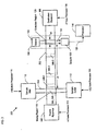
- FIG. 3 depicts a schematic diagram of details of a CE system in accordance with an illustrative embodiment of the present invention.
- CE system 300 comprises flow channel 302, source reservoir 104, destination reservoir 106, sample channel 304, sample inlet 110, sample outlet 112, processor 114, and sensor 116.
- CE system 300 is analogous to the operation of CE system 100.
- the flow of analyte plug 308 along length d1 of flow channel 304 proceeds substantially free of the deformation that characterizes the flow of analyte plug 132 through flow channel 102, as described above and with respect to FIG. 1 .
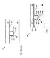
- FIG. 4 depicts a cross-sectional view of flow channel 302, in accordance with the illustrative embodiment of the present invention.
- Flow channel 302 comprises trench 402 and cover plate 404.
- Trench 402 is formed in substrate 406 and comprises sidewalls 408 and 410, and bottom 412.
- microfluidic channels formed in borophosphosilicate are known in the prior art.
- Callender, et al . have disclosed borophosphosilicate glass microchannels in publications including " Microchannel Arrays in Borophosphosilicate Glass for Photonic Device and Optical Sensor Applications," Materials Research Symposium Proceedings, Vol. 872, pp. J16.3.1-J16.3.6 (2005 ).
- Such borophosphosilicate microfluidic channels are limited to a circular or elliptical cross-sectional shape within a narrow size range. This limitation arises from the manner in which they are formed.
- they are formed by depositing a thick layer of borophosphosilicate glass in a manner that produces an intentional void in the middle of the borophosphosilicate layer. This layer is then annealed to reflow the borophosphosilicate material, thereby inducing the void to form into an elliptical or circular cross-sectional shape.
- the present invention enables formation of microfluidic channel with any desired cross-sectional shape.
- the present invention enables design of a microfluidic channel with nearly any desirable set of geometrically determined flow characteristics.
- FIG. 5 depicts a method for forming a microfluidic channel in accordance with the illustrative embodiment of the present invention. Method 500 is described herein with continuing reference to FIGS. 3 and 4 .
- Method 500 begins with operation 501, wherein trench 402 is formed in substrate 406.
- Substrate 406 is a 100 mm-diameter wafer of fused silica and has a thickness of approximately 500 microns.
- substrate 406 is a material other than fused silica.
- substrate 406 is a material other than fused silica and includes a layer of fused silica disposed on at least one surface, wherein trench 402 is formed in this layer.
- Trench 402 is formed using conventional methods, such as DRIE, reactive ion etching, wet etching, single-point diamond machining, sand blasting, or laser-assisted etching.
- Trench 402 has a substantially u-shape with feature sizes within the range of approximately 25-200 microns per side.
- trench 402 has a different shape, such as an open-topped rectangle, triangle, trapezoid, semicircle, semi-oval, and the like.
- layer 418 is deposited on substrate 406.
- Layer 418 is a layer of borophosphosilicate glass (BPSG) having a thickness within the range of approximately 10 nanometers (nm) to approximately 5 microns. In some embodiments, the thickness of layer 418 is approximately 1 micron.
- Layer 418 is deposited using low-pressure chemical vapor deposition (LPCVD) to form a conformal coating. As a result, layer 418 is disposed, with substantially uniform thickness, on surfaces 414, 408, 410, and 412 of substrate 406.
- the interior surface of trench 402 comprises surfaces 422, 424, and 426, which are all BPSG surfaces.
- the formation of layer 420 results in a smoothing of the surface to which the analyte plug is exposed. As a result, the analyte plug is less susceptible to smearing out as it flows along the microchannel.
- layer 420 is formed on cap layer 404.
- Layer 420 is a layer of BPSG having a thickness within the range of approximately 10 nm to approximately 5 microns. In some embodiments, the thickness of layer 420 is approximately 1 micron.. In some embodiments, cap layer 404 is a wafer of fused silica having a thickness of approximately 500 microns.
- the illustrative embodiment comprises layers 418 and 420 that each have a thickness of approximately 1 micron, it will be clear to one skilled in the art, after reading this specification, how to specify, make, and use alternative embodiments of the present invention wherein at least one of layers 418 and 420 has a different thickness. It will also be clear, after reading this specification, how to make and use alternative embodiments of the present invention wherein a portion of at least one of layers 418 and 420 is removed using conventional techniques.
- cover plate 404 is attached to substrate 406 by means of fusion bonding. Once cover plate 404 and substrate 406 are attached, flow channel 302 is fully formed and has an interior surface that is exclusively BPSG. As a result, the electrokinetic potential of the interior surfaces of flow channel 302 is well-matched to that of the analyte included in analyte plug 308. In some embodiments, cover plate 404 is attached to substrate 406 by means of thermo-anodic bonding.
Landscapes
- Chemical & Material Sciences (AREA)
- Health & Medical Sciences (AREA)
- Life Sciences & Earth Sciences (AREA)
- Chemical Kinetics & Catalysis (AREA)
- Analytical Chemistry (AREA)
- Molecular Biology (AREA)
- General Health & Medical Sciences (AREA)
- General Physics & Mathematics (AREA)
- Hematology (AREA)
- Physics & Mathematics (AREA)
- Electrochemistry (AREA)
- Immunology (AREA)
- Pathology (AREA)
- Dispersion Chemistry (AREA)
- Biochemistry (AREA)
- Clinical Laboratory Science (AREA)
- Engineering & Computer Science (AREA)
- General Chemical & Material Sciences (AREA)
- Geochemistry & Mineralogy (AREA)
- Materials Engineering (AREA)
- Organic Chemistry (AREA)
- Optical Measuring Cells (AREA)
- Automatic Analysis And Handling Materials Therefor (AREA)
Applications Claiming Priority (1)
| Application Number | Priority Date | Filing Date | Title |
|---|---|---|---|
| US12/172,740 US8454811B2 (en) | 2008-07-14 | 2008-07-14 | Microfluidic system |
Publications (1)
| Publication Number | Publication Date |
|---|---|
| EP2146201A1 true EP2146201A1 (fr) | 2010-01-20 |
Family
ID=41168403
Family Applications (1)
| Application Number | Title | Priority Date | Filing Date |
|---|---|---|---|
| EP09009124A Ceased EP2146201A1 (fr) | 2008-07-14 | 2009-07-13 | Système micro fluide avec revêtement de surface |
Country Status (2)
| Country | Link |
|---|---|
| US (1) | US8454811B2 (fr) |
| EP (1) | EP2146201A1 (fr) |
Citations (2)
| Publication number | Priority date | Publication date | Assignee | Title |
|---|---|---|---|---|
| WO2007139511A1 (fr) * | 2006-05-31 | 2007-12-06 | Agency For Science, Technology And Research | Dispositif microfluidique transparent |
| WO2008065868A1 (fr) * | 2006-12-01 | 2008-06-05 | Konica Minolta Opto, Inc. | Procédé de liaison de substrat de micropuce et micropuce |
Family Cites Families (2)
| Publication number | Priority date | Publication date | Assignee | Title |
|---|---|---|---|---|
| US6210986B1 (en) | 1999-09-23 | 2001-04-03 | Sandia Corporation | Microfluidic channel fabrication method |
| WO2007108773A1 (fr) * | 2006-03-23 | 2007-09-27 | Agengy For Science, Technology And Research | Dispositif d'analyse de l'état d'une particule |
-
2008
- 2008-07-14 US US12/172,740 patent/US8454811B2/en not_active Expired - Fee Related
-
2009
- 2009-07-13 EP EP09009124A patent/EP2146201A1/fr not_active Ceased
Patent Citations (3)
| Publication number | Priority date | Publication date | Assignee | Title |
|---|---|---|---|---|
| WO2007139511A1 (fr) * | 2006-05-31 | 2007-12-06 | Agency For Science, Technology And Research | Dispositif microfluidique transparent |
| WO2008065868A1 (fr) * | 2006-12-01 | 2008-06-05 | Konica Minolta Opto, Inc. | Procédé de liaison de substrat de micropuce et micropuce |
| EP2096445A1 (fr) * | 2006-12-01 | 2009-09-02 | Konica Minolta Opto, Inc. | Procédé de liaison de substrat de micropuce et micropuce |
Non-Patent Citations (4)
| Title |
|---|
| "Microchannel Arrays in Borophosphosilicate Glass for Photonic Device and Optical Sensor Applications", MATERIALS RESEARCH SYMPOSIUM PROCEEDINGS, vol. 872, 2005, pages J16.3.1 - J16.3.6 |
| BARNES T J ET AL: "PEO-PPO-PEO block copolymers at the emulsion droplet-water interface", LANGMUIR 20000502 ACS, vol. 16, no. 9, 2 May 2000 (2000-05-02), pages 4116 - 4121, XP002554061 * |
| BRIAN J. KIRBY ET AL: "Programmable modification of cell adhesion and zeta potential in silica microchips", LAB ON A CHIP, vol. 3, no. 1, 1 January 2003 (2003-01-01), pages 5 - 10, XP055093463, ISSN: 1473-0197, DOI: 10.1039/b210621n * |
| CHIA-YEN LEE ET AL: "Band spreading control in electrophoresis microchips by localized zeta-potential variation using field-effect", THE ANALYST, vol. 129, no. 10, 1 January 2004 (2004-01-01), pages 931, XP055006489, ISSN: 0003-2654, DOI: 10.1039/b407627n * |
Also Published As
| Publication number | Publication date |
|---|---|
| US20100006435A1 (en) | 2010-01-14 |
| US8454811B2 (en) | 2013-06-04 |
Similar Documents
| Publication | Publication Date | Title |
|---|---|---|
| Kim et al. | Nanofluidic concentration devices for biomolecules utilizing ion concentration polarization: theory, fabrication, and applications | |
| US6149787A (en) | External material accession systems and methods | |
| US7261824B2 (en) | Method of fabrication of a microfluidic device | |
| Edgar et al. | Capillary electrophoresis separation in the presence of an immiscible boundary for droplet analysis | |
| US20110147215A1 (en) | Method and device for manipulating and observing liquid droplets | |
| Jeon et al. | Continuous particle separation using pressure-driven flow-induced miniaturizing free-flow electrophoresis (PDF-induced μ-FFE) | |
| WO2002068821A9 (fr) | Commande par microfluides utilisant le pompage dielectrique | |
| US20020180963A1 (en) | Microfluidic systems with enhanced detection systems | |
| WO2007092253A2 (fr) | dispositifs microfluidiques electro-osmotiques a charge induite | |
| US20100072078A1 (en) | Micro-device for analysing liquid samples | |
| Oh et al. | Monitoring FET flow control and wall adsorption of charged fluorescent dye molecules in nanochannels integrated into a multiple internal reflection infrared waveguide | |
| CN109937092B (zh) | 具有微珠集成系统的微流体芯片和芯片中集成受体的方法 | |
| US8974650B2 (en) | Microfluidic system | |
| Evstrapov et al. | Application of porous glasses in microfluidic devices | |
| Sung et al. | Development of a nanofluidic preconcentrator with precise sample positioning and multi-channel preconcentration | |
| EP1151290B1 (fr) | Appareil et procedes pour la separation a haute resolution de composes d'echantillon sur dispositifs de canaux micro-fabriques | |
| US8454811B2 (en) | Microfluidic system | |
| US8330953B2 (en) | Detection method and detection apparatus | |
| US20140001116A1 (en) | Microfluidic extraction device having a stabilized liquid/liquid interface | |
| KR100486730B1 (ko) | 교류 전압과 t 채널을 이용하여 제타 포텐셜을 측정하는방법 | |
| Mawatari et al. | Extended nanospace chemical systems on a chip for new analytical technology | |
| ES2731693T3 (es) | Sistema de evacuación de gas para biosensor nanofluídico | |
| Kutter et al. | Microfluidics--Components | |
| JP5483616B2 (ja) | フローセルおよびフローセルの送液方法 | |
| WO2024129639A1 (fr) | Dispositif de capteur avec cavité fluidique fonctionnalisée |
Legal Events
| Date | Code | Title | Description |
|---|---|---|---|
| PUAI | Public reference made under article 153(3) epc to a published international application that has entered the european phase |
Free format text: ORIGINAL CODE: 0009012 |
|
| AK | Designated contracting states |
Kind code of ref document: A1 Designated state(s): AT BE BG CH CY CZ DE DK EE ES FI FR GB GR HR HU IE IS IT LI LT LU LV MC MK MT NL NO PL PT RO SE SI SK SM TR |
|
| AX | Request for extension of the european patent |
Extension state: AL BA RS |
|
| 17P | Request for examination filed |
Effective date: 20100720 |
|
| 17Q | First examination report despatched |
Effective date: 20110119 |
|
| 18R | Application refused |
Effective date: 20171207 |