EP2146287B1 - Schnittstelle zwischen einem Doppelleitungsbus und einem Einzelleitungsbus - Google Patents
Schnittstelle zwischen einem Doppelleitungsbus und einem Einzelleitungsbus Download PDFInfo
- Publication number
- EP2146287B1 EP2146287B1 EP09163517A EP09163517A EP2146287B1 EP 2146287 B1 EP2146287 B1 EP 2146287B1 EP 09163517 A EP09163517 A EP 09163517A EP 09163517 A EP09163517 A EP 09163517A EP 2146287 B1 EP2146287 B1 EP 2146287B1
- Authority
- EP
- European Patent Office
- Prior art keywords
- bus
- wire
- circuit
- signal
- scl
- Prior art date
- Legal status (The legal status is an assumption and is not a legal conclusion. Google has not performed a legal analysis and makes no representation as to the accuracy of the status listed.)
- Active
Links
Images


Classifications
-
- G—PHYSICS
- G06—COMPUTING OR CALCULATING; COUNTING
- G06F—ELECTRIC DIGITAL DATA PROCESSING
- G06F13/00—Interconnection of, or transfer of information or other signals between, memories, input/output devices or central processing units
- G06F13/38—Information transfer, e.g. on bus
- G06F13/42—Bus transfer protocol, e.g. handshake; Synchronisation
- G06F13/4282—Bus transfer protocol, e.g. handshake; Synchronisation on a serial bus, e.g. I2C bus, SPI bus
-
- G—PHYSICS
- G06—COMPUTING OR CALCULATING; COUNTING
- G06F—ELECTRIC DIGITAL DATA PROCESSING
- G06F13/00—Interconnection of, or transfer of information or other signals between, memories, input/output devices or central processing units
- G06F13/38—Information transfer, e.g. on bus
- G06F13/40—Bus structure
- G06F13/4004—Coupling between buses
- G06F13/4027—Coupling between buses using bus bridges
-
- G—PHYSICS
- G06—COMPUTING OR CALCULATING; COUNTING
- G06F—ELECTRIC DIGITAL DATA PROCESSING
- G06F2213/00—Indexing scheme relating to interconnection of, or transfer of information or other signals between, memories, input/output devices or central processing units
- G06F2213/0016—Inter-integrated circuit (I2C)
Definitions
- the present invention relates to electronic circuits and, more particularly, the transmission of digital data between two circuits in a master-slave type system.
- the invention applies more particularly to the conversion of digital signals between a first bus of two-wire type (data and clock) and a second bus of single-wire type.
- An object of the present invention is to overcome all or part of the disadvantages that hinder the compatibility of communications between a two-wire bus and a single-wire bus.
- An embodiment is more particularly aimed at a solution in a master-slave type communication system where the single-wire bus also carries power to one of the circuits.
- an embodiment provides a method of converting a first bus having at least one data wire and a clock wire into a single-wire bus, in which one bit data of the first bus is converted, on a half-period of the clock signal for transmission on the second bus, a waiting pattern being placed on the second bus during the other half-period.
- the waiting pattern is present on each first half-period of the signal present on the clock wire during a transmission of the second bus to the first bus and on each second half. period of the signal present on the clock wire for a transmission in the other direction.
- the waiting pattern is a pulse train of fixed duration.
- the waiting pattern corresponds to a repetition of the transmitted bit.
- a bit of data to be transmitted from the first bus to the second bus is positioned on the second bus at the appearance of a rising edge on the clock wire of the first bus.
- a data bit to be transmitted from the second bus to the first bus is positioned, on the data wire of the first bus, to the appearance of a rising edge on the clock wire. of the first bus.
- an acknowledgment pattern arriving on the second bus in a second half-period of the signal present on the clock wire, is converted to be transmitted over the data wire of the present invention.
- first bus on the next rising edge of this signal.
- a device for converting a transmission between a first bus comprising at least one data wire and a clock wire, and a second single-wire bus.
- a master-slave communication system between a first device capable of communicating on an I2C bus and a second device capable of communicating on a single-wire bus, comprising at least one such conversion device.
- the first device is a printer and the second device is an ink cartridge.
- the embodiments will subsequently refer to a communication between a master device using a protocol known as I2C and a slave device using a single-line protocol of the type described in US 5,903,607 and European patents. 0 798 901 .
- the invention more generally applies to any communication protocol using two-wire bus side, a data wire and a clock wire (for example, the protocol known as SPI). It also applies to any protocol sharing a single-wire bus for data and a clock signal (for example, the protocol known as SWP-Single Wire Protocol).
- the figure 1 is a block diagram of an embodiment of a communication system between a circuit 1 capable of transmitting data according to the I2C protocol and other circuits among which at least one circuit 2 capable of communicating according to a single-line protocol SW .
- the circuit 1 is a master circuit (MD) and is capable of communicating, on the I2C bus side, with one or more slave devices 3 (SD).
- the I2C bus is connected to a conversion circuit (CONV) to a single-wire bus SW.
- Bus side SW one or more circuits 2 of slave type are likely to be connected.
- the various circuits of the system may be powered independently of each other or, as shown, at least the circuits 1, 3 and 5 are powered by a power supply bus capable of carrying at least one VDD supply potential and a reference potential GND, for example mass. Side circuits 2, they are connected to a potential reference that can be the same (GND) as other circuits or be a different mass. In the latter case, the conversion circuit 5 is provided with an isolation barrier. According to another variant, the circuits 2 are also powered independently of the bus SW, for example by the voltage VDD or other.
- the figure 2 is a partial block diagram showing circuits 1 and 3 of the figure 1 .
- Each circuit 1, 3 comprises, for example, a transmission circuit (SEND) 11, 31 and a reception circuit (DET) 12, 32.
- the circuits 1 and 3 are connected to each other by the bus I2C as well as the two VDD and GND wires of the power bus.
- a first SCL wire of the I2C bus carries an SCL clock signal between two clock terminals CK of the circuits 1 and 3. Typically, this clock signal is imposed by the master circuit 1.
- a second wire SDA of the bus I2C vehicle the data between the two circuits.
- the I2C bus is bidirectional.
- FIGS. 3A, 3B, 3C and 3D are timing diagrams illustrating a communication between circuits 1 and 3 of the figure 2 . These figures illustrate an example of transmission of a word (typically a byte) of data from the master circuit 1 to the slave circuit 3.
- a word typically a byte
- the Figures 3A, 3C and 3D represent the appearance of signals SDAM, SDAS and SDA respectively corresponding to the signal positioned by the transmission circuit 11 of the master circuit on the wire SDA, the signal positioned by the circuit 31 on this wire, and the resulting level of this wire SDA .
- the two SCL and SDA wires of the I2C bus are high.
- the circuit 1 wants to transmit a data frame to the circuit 3, it takes control of the bus by imposing a low level on the SDA signal (time t1) while the SCL signal remains high.
- the master circuit 1 generates the clock signal SCL.
- the circuit 1 imposes a level 1 or 0 on the SDA wire according to the first bit D7 of the byte to be transmitted. This positioning of the level of the SDA wire must occur before the rising edge of the clock signal (time t2) which validates the data transmitted.
- the master circuit 1 can impose the level corresponding to the state of the next bit D6 on the SDA wire, and so on.
- the master circuit places the signal SDAM high, to monitor the arrival of an acknowledgment. Its detection circuit 12 at the same time monitors the actual state of the SDA wire.
- the slave circuit 3 imposes a low level ( figure 3C ) on the SDA wire.
- the master circuit verifies the state of the SDA wire at the rising edge (time t4) of the SCL signal which follows its positioning in the high state of the SDAM signal. If the SDA wire is low (as shown in figure 3 ), it means a successful transmission.
- a transmission end is performed by the master circuit by switching the SDA wire high while the SCL signal is also high (time t5). Once this stop condition is completed, the I2C bus is free to start another I2C frame. It may be for example a transmission of the circuit 3 to the circuit 1.
- the communication protocol I2C sets different additional conditions in the transmission depending on whether it concerns an address, a data, a writing or a reading in the slave circuit, etc.
- an I2C bus operates most often by releasing the bus for the high state and forcing in the low state.
- the figure 4 is a partial block diagram showing the circuits 2 of the figure 1 assuming that one of them (noted 2 'in figure 4 ) imposes on the other a communication according to a single-slave master-slave protocol.
- each circuit 2 or 2 ' comprises a transmitting circuit (SEND) 21, 21' and a receiving circuit (DET) 22, 22 'capable of being connected to the single wire S of the SW bus.
- the two circuits 2 and 2 'further share a reference potential link (typically GND ground).
- the circuit 2' imposes a signal SM on the bus.
- the circuit 2 imposes a signal SS on the bus.
- the circuit that causes the transmission imposes the clock on the bus.
- we have schematized in figure 4 the signals SM and SS as respectively coming from the circuits 21 'and 21 and it is considered that the circuits 22' and 22 only see the state of the signal S.
- the figure 5 is a timing diagram showing an example of the shape of the signal S imposed by the master circuit 2 'illustrating a communication between the circuits 2' and 2.
- the single-wire protocol is to transmit on the bus both a clock signal or synchronization and data.
- the master circuit 2 generally supplies the slave circuit 2 as illustrated in FIG. figure 4 where only the master circuit 2 'receives the power supply potential VDD.
- the slave circuit derives its power from a filtering of the signal S whose rest level imposed by the master circuit is a high level V1.
- the circuit 2' modulates the signal SM in amplitude between two levels V1 and V0, for example both positive, according to a predefined coding. This modulation is found on the signal S.
- a transmission is initialized by a start bit START in which the signal S is forced (time t5) at the level V0. This initializes the slave circuit 2 and prepares it to receive data.
- the master circuit 2 ' modulates the level of the signal S at the rate of a clock signal which sets the transmission rate.
- the transmission of a bit at level 0 is effected, for example, with a level V1 pulse lower than the half-period of the clock signal (for example, a quarter of the period) while a level 1 is coded with a V1 level pulse greater than the half-period of this clock signal (for example, three quarters of the period).
- the slave circuit detects the amplitude variation and the corresponding duration of the high and low pulses to determine the value of the transmitted bits.
- the slave circuit modifies the load that it imposes on the wire S according to the level of the bit that it wishes to transmit.
- the transmission rate is set by a clock signal at the rate of which the circuit 2 modulates the amplitude of the signal S.
- the clock is here fixed by an internal clock of the circuit 2 while the level (V1) rest of the bus remains fixed by the circuit 2 '.
- the I2C and SW buses are both two-way (half-duplex or half-duplex) communication buses.
- the role of circuit 5 ( figure 1 ) of conversion or interface is, in a way, to transform a transmission of the circuit 1 of the figure 2 for it to be seen by circuit 2 as if it came from a circuit 2 '( figure 4 ), and to transform a transmission of the circuit 2 of the figure 4 to be seen by Circuit 1 as if it came from Circuit 3 ( figure 2 ).
- FIGS. 6A, 6B and 6C illustrate an example of what could be done by an interface circuit between an I2C bus and a single-wire bus.
- a critical point is that, on the I2C bus side, it the acknowledgment bit must be detected at the end of a frame.
- To the Figures 6A to 6C only the end of such a frame has been illustrated by the transmission of a 1 and then a 0 on the SDA signal, supposed to be converted on the single-wire bus side with pulse shapes of the type illustrated in FIG. figure 5 .
- the master circuit communicating according to the I2C protocol sets the high-level SDA wire (time t10) and simultaneously monitors the level of this wire to detect a low-level forcing caused by the circuit slave indicating a correct transmission. If, at the rising edge which follows (instant t11) of the signal SCL, the signal SDA has not been pulled low by the slave circuit, the master circuit considers an incorrect transmission.
- the slave circuit could not, with the protocol of the figure 5 , position a signal corresponding to an acknowledgment-reception (for example, the equivalent of the transmission of a 0) so that it is interpreted by the interface and transmitted on the I2C bus side, that from this moment t11 which follows the last bit of the data it receives (in this example a state 0). Therefore, the SDA signal would be pulled low only at the next rising edge (time t12) of the SCL signal. At time t11, the master circuit would therefore interpret an absence of acknowledgment (NACK).
- NACK absence of acknowledgment
- the figure 7 represents, in block form, an embodiment of a conversion circuit 5 between an I2C bus and a SW bus.
- the circuit 5 is supplied on the I2C bus side (for example, by the master circuit) and that the bus-side circuit SW derives its power from the signal S.
- the circuit 5 is, for example, embodied in the form of a processor (e.g., a microprocessor) capable of executing software instructions representative of a data conversion algorithm between the two buses.
- the circuit 5 is a circuit representing a state machine in hardwired logic.
- this circuit 5 is an integrated circuit ASIC, a microcontroller, a programmable gate array (FPGA). All these circuits have their own internal clock.
- the figure 8 illustrates an example of SW bus side coding performed by the conversion circuit.
- a predetermined pattern consisting, in this example, of a train of pulses representing two pulses at the high level (V1) over 1/8 of the period SCL T, is used to complete the useful signal in the first A or second B half-period of the SCL signal.
- the IDLE pattern is generated by the circuit 5 so that the transmission by the devices connected to this circuit is not changed.
- a start bit transmitted by the I2C bus is converted to a high level (V1) during a first half-period A of the SCL signal and is followed in the second half-period B of the IDLE pattern.
- a bit in state 1 respects the coding of the protocol SW with a pulse in the state V1 representing 3/4 of the useful period (1/2 period of the signal SCL).
- a bit in state 0 corresponds to a level V1 during 1/4 of the useful period.
- the same pattern is used to transmit, from the slave device, an acknowledgment bit ACK.
- a bit of absence of acknowledgment NACK is represented by a permanent high level on the useful period (half-period of the signal SCL) insofar as the state of rest of the bus SW is the high level V1.
- a stop bit is represented, over an entire SCL period T SCL of the signal SCL, by the IDLE pattern followed by a low level in the second half-period B.
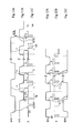
- FIGS 9A, 9B and 9C are chronograms illustrating an example of conversion, by element 5 of the figure 7 , a transmission of one byte of data from the I2C bus to the bus SW.
- FIGS 9A to 9C we assume patterns as illustrated by the figure 8 .
- the circuit 5 detects a switching (instant t21) in the low state of the signal SDA while the signal SCL remains high, which identifies a starting condition of the bus I2C. This detection causes the generation, by the circuit 5, of a communication start pattern START on the wire S. At the following falling edge (time t22) of the signal SCL on the bus I2C, the element 5 positions a signal pattern. IDLE wait on wire S for half a period of the SCL clock. During this half-period, arrives in the usual way on the SDA signal, the positioning of the first bit of data to be transmitted (time t23). In this example, a first bit in state 1 is assumed.
- the rising edge of the following signal SCL causes positioning, by circuit 5, of a bit pattern at state 1 for half a second. -period of the signal SCL on the signal S.
- the element 5 positions the waiting pattern IDLE. This operation continues until the transmission of the last bit of the word (instant t26) which is followed by the arrival on the I2C bus of an acknowledgment request by a positioning of the signal SDA (time t28) to the high state and monitoring, by the circuit connected on this bus, the state of this signal to detect the arrival of an acknowledgment-receipt.
- the slave circuit connected to the bus SW sets according to the single-wire protocol an acknowledgment bit ACK on the falling edge (instant t27) of the signal SCL which immediately follows the rising edge. having positioned the last bit.
- the ACK pattern prevails over the IDLE pattern (where the IDLE pattern is at the level V0, the pattern ACK must be too).
- the element 5 also positions an IDLE wait pattern on the single-wire bus SW to allow the slave circuit to respond to the master circuit. Furthermore, the circuit 5 releases the SDA wire, for example at a time t30, before the next falling edge of the SCL signal.
- all the patterns of the signal S are positioned by the element 5 with the exception of the acknowledgment-representation pattern illustrated in dashed lines ( Figure 9C ) at time t27 which comes from the slave circuit.
- all the patterns are set by the master device except for switching at time t29 of the SDA signal to the low state which is caused by the conversion circuit 5 having interpreted the acknowledgment pattern. receiving the slave device, and releasing the SDA wire at time t30.
- the master circuit keeps the SDA wire low (canceling the effect caused by the conversion circuit at time t30), then causes a switch in the high state of the SDA signal on a high-level period of the SCL signal, allowing the circuit 5 to send a stop pattern to the slave circuit.
- the Figures 10A, 10B and 10C illustrate an example of a return transmission from the slave device connected on the single-wire bus to the master device of the I2C bus. It is assumed that following the master-slave transmission of Figures 9A to 9C , the circuit 5 releases the I2C bus at time t30. Thus, the signal SDA returns to the high state on the bus I2C corresponding to its state of rest. Slave device side, it starts a transmission from the next falling edge (time 31) of the SCL signal and sets its first response bit.
- the circuit 2 transmits coded bits by the length of the pulse at the level V1. It fixes, thanks to its internal clock circuits, the shape of the patterns communicated towards the circuit 5.
- the frequency is however chosen to be greater than the frequency of the SCL signal so that it can encode the data like this. is illustrated, for example, in figure 8 . Since the circuit 2 receives the frequency of the signal SCL by the circuit 5, it can adjust its transmission frequency accordingly. The circuit 5 then interprets the pulse length variations on the signal S to convert them, SDA wire side, and act as master bus side I2C. In the example shown, the positioning of the first bit corresponds to a pattern 0 over half a period of the SCL signal.
- the element 5 transmits the first bit to the state 0 that it has interpreted from the single-wire bus to the signal SDA by switching it to the low state by the same time that it sets the IDLE wait pattern on the SW bus.
- the following falling clock edge results in the device 5 reading the following pattern (for example state 1) present on the signal S.
- the circuit 5 sets this bit on the I2C bus at the front next amount (time t34) of the SCL signal, and so on until the end of transmission of the byte concerned.
- the patterns of the signal S positioned by the circuit 5 have been illustrated in solid lines while the patterns positioned by the circuit 2 have been illustrated in dotted lines.
- the circuit 5 At the rising edge of the signal SCL (time t35) which follows the reception, by the circuit 5, of the last bit of the transmitted word, it places the waiting bit on the wire S. Then, on the falling edge which follows (instant t36), it reposition a wait bit on the second part of the period of the SCL signal. This allows the switching to the low state of the SDA signal, caused by the device 1 at the next rising edge (time t37) of the SCL signal, is interpreted by the element 5 as an acknowledgment-receipt. The circuit 5 then positions, on the single-wire bus SW, the acknowledgment-ACK pattern (corresponding to a bit in state 0).
- the IDLE wait pattern is therefore set either on the first half-period of the SCL signal or on the second half-period. This allows in both directions to be able to correctly interpret an acknowledgment bit.
- the implementation proposed does not require any modification of the master device, this implementation being transparent for it.
- the slave device side it must be able to interpret the wait pattern, sequence the bits, and return the ACK pattern in a manageable sequence for real-time conversion. In fact, it manages one channel to represent bits and another channel for IDLE patterns and channel swapping to transmit in the other direction in time for conversion to the I2C bus.
- the Figures 11A, 11B and 11C and the Figures 12A, 12B and 12C illustrate another example of transmission in the master-slave direction then slave-master.
- This example shows another change that is a different wait pattern from the one shown in figure 8 .
- the waiting pattern generated by the converter 5 is here a pulse in the low state (V0 level) in the vicinity of the beginning of the pattern.
- This pattern is chosen to have a duration Tp less than the half-period of the SCL signal.
- the conversion circuit 5 detects (instant t21) a starting condition on the I2C bus which it sends on the single-wire bus. As soon as the first falling edge (instant t22) of the signal SCL arrives, the circuit 5 positions the waiting pattern on the single-wire bus. Then, at the next rising edge (time t24), causes the pattern corresponding to the first bit transmitted to follow. As illustrated by figure 11C , the waiting pattern does not go to the rising edge of the SCL signal.
- the slave device sets the acknowledgment-reception pattern (time t28) on the single-wire bus. As it is synchronized by the decoding of the bits it receives, this transmission is also synchronized to the SCL signal. At the next rising edge (time t29), the element 5 forces the signal SDA to the low state thus allowing detection by the master device. In a similar manner to the previous example, it is assumed that the direction of transmission is inverted at time t29.
- Figures 12A to 12C illustrate the transmission of a byte in the slave-master direction. The operation is deduced from that explained in relation with the preceding figures.
- the second channel (half-period of the SCL signal) is used to repeat the transmitted bit. It then serves as redundancy.
- the waiting pattern is then variable in shape, duration and / or in the direction of transmission.
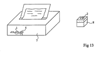
- the figure 13 is a block diagram illustrating, very schematically, an example of application of the described communication system to communications between a printer 7 and one or more ink cartridges 8.
- the cartridge 8 has been shown out of the printer 7 but, when it must communicate with it, it is of course a cartridge positioned in the printer.
- the printer 7 is equipped with one or more electronic cards 71 comprising at least one circuit 1 intended to behave in a master circuit for communicating with one or more cartridges 8.
- the cartridge or cartridges each comprise a circuit 2 capable of communicating according to a single-line protocol.
- one of the electronic circuit cards 71 of the printer comprises at least one hardware or software conversion circuit for converting transmissions on a printer-side I2C bus into transmissions. on a single-wire bus to a circuit 2 of one or more cartridges.
- the conversion circuit 5 is placed on the cartridge side and not on the printer side.
- the above example makes it possible to use simplified circuits in the cartridges 8 by operating a single-wire bus and to make them compatible with printers capable of communicating only through an I2C bus.
Landscapes
- Engineering & Computer Science (AREA)
- Theoretical Computer Science (AREA)
- General Engineering & Computer Science (AREA)
- Physics & Mathematics (AREA)
- General Physics & Mathematics (AREA)
- Computer Hardware Design (AREA)
- Dc Digital Transmission (AREA)
- Small-Scale Networks (AREA)
- Information Transfer Systems (AREA)
- Bus Control (AREA)
Claims (9)
- Ein Verfahren zum Konvertieren eines ersten Busses (12C), der wenigstens eine Datenleitung (SDA) und eine Taktleitung (SCL) aufweist, in einen Einzelleitungsbus (SW), wobei das Verfahren die folgenden Schritte aufweist:ein Datenbit des ersten Busses wird während einer Halbperiode des Taktsignals zum Übertragen über den zweiten Bus konvertiert, undein Wartemuster (IDLE) wird während der anderen Halbperiode auf dem zweiten Bus gesetzt, wobei das Wartemuster (IDLE) in jeder ersten Halbperiode (A) des Signals anwesend ist, das auf der Taktleitung (SCL) anwesend ist, in einer Übertragung von dem zweiten Bus (SW) zu dem ersten Bus (12C) und in jeder zweiten Halbperiode (B) des Signals, das auf der Taktleitung (SCL) anwesend ist, für eine Übertragung in der anderen Richtung.
- Das Verfahren nach Anspruch 1, wobei das Wartemuster (IDLE) eine Impulsfolge von festgelegter Dauer ist.
- Das Verfahren nach Anspruch 1, wobei das Wartemuster einer Wiederholung des übertragenen Bits entspricht.
- Das Verfahren nach einem der Ansprüche 1 bis 3, wobei ein zu übertragendes Datenbit von dem ersten Bus (12C) zu dem zweiten Bus (SW) auf dem zweiten Bus, beim Auftreten einer ansteigenden Flanke auf der Taktleitung (SCL) des ersten Busses, gesetzt wird.
- Das Verfahren nach einem der Ansprüche 1 bis 4, wobei ein zu übertragendes Datenbit von dem zweiten Bus (SW) zu dem ersten Bus (12C) auf der Datenleitung (SDA) des ersten Busses, beim Auftreten einer ansteigenden Flanke auf der Taktleitung (SCL) des ersten Busses, gesetzt wird.
- Das Verfahren nach einem der Ansprüche 1 bis 5, wobei ein Bestätigungsmuster, das auf dem zweiten Bus (SW) in einer zweiten Halbperiode des Signals, das auf der Taktleitung (SCL) anwesend ist, ankommt, konvertiert wird, um über die Datenleitung (12C) des ersten Busses auf der nächsten ansteigenden Flanke des Signals übertragen zu werden.
- Eine Vorrichtung zum Konvertieren einer Übertragung zwischen einem ersten Bus (12C), der wenigstens eine Datenleitung (SDA) und eine Taktleitung (SCL) aufweist, und einem zweiten Einzelleitungsbus (SW), wobei die Vorrichtung Mittel zum Implementieren des Verfahrens nach einem der Ansprüche 1 bis 6 aufweist.
- Ein Master-Slave Kommunikationssystem zwischen einer ersten Vorrichtung (1), die geeignet ist über einen 12C Bus zu kommunizieren und einer zweiten Vorrichtung (2), die geeignet ist über einen Einzelleitungsbus zu kommunizieren, wobei das Kommunikationssystem wenigstens eine Konvertierungsvorrichtung (5) nach Anspruch 7 aufweist.
- Das System nach Anspruch 8, wobei die erste Vorrichtung ein Drucker (7) ist und die zweite Vorrichtung eine Tintenpatrone (8) ist.
Applications Claiming Priority (1)
| Application Number | Priority Date | Filing Date | Title |
|---|---|---|---|
| FR0854820 | 2008-07-16 |
Publications (2)
| Publication Number | Publication Date |
|---|---|
| EP2146287A1 EP2146287A1 (de) | 2010-01-20 |
| EP2146287B1 true EP2146287B1 (de) | 2012-01-25 |
Family
ID=40303758
Family Applications (1)
| Application Number | Title | Priority Date | Filing Date |
|---|---|---|---|
| EP09163517A Active EP2146287B1 (de) | 2008-07-16 | 2009-06-23 | Schnittstelle zwischen einem Doppelleitungsbus und einem Einzelleitungsbus |
Country Status (3)
| Country | Link |
|---|---|
| US (1) | US8161224B2 (de) |
| EP (1) | EP2146287B1 (de) |
| AT (1) | ATE543139T1 (de) |
Families Citing this family (68)
| Publication number | Priority date | Publication date | Assignee | Title |
|---|---|---|---|---|
| FR2939926B1 (fr) * | 2008-12-17 | 2010-12-10 | St Microelectronics Rousset | Transmission sur bus i2c |
| US9112452B1 (en) | 2009-07-14 | 2015-08-18 | Rf Micro Devices, Inc. | High-efficiency power supply for a modulated load |
| US8633766B2 (en) | 2010-04-19 | 2014-01-21 | Rf Micro Devices, Inc. | Pseudo-envelope follower power management system with high frequency ripple current compensation |
| US8519788B2 (en) | 2010-04-19 | 2013-08-27 | Rf Micro Devices, Inc. | Boost charge-pump with fractional ratio and offset loop for supply modulation |
| EP2782246B1 (de) | 2010-04-19 | 2018-06-13 | Qorvo US, Inc. | Energieverwaltungssystem mit Pseudo-Hüllkurvenfolger |
| US8866549B2 (en) | 2010-06-01 | 2014-10-21 | Rf Micro Devices, Inc. | Method of power amplifier calibration |
| CN101895425B (zh) * | 2010-07-13 | 2014-03-12 | 中兴通讯股份有限公司 | 一种主备无缝切换装置和方法 |
| FR2963449B1 (fr) * | 2010-07-27 | 2013-01-25 | St Microelectronics Rousset | Conversion d'un bus bifilaire en bus unifilaire |
| FR2963519B1 (fr) | 2010-07-27 | 2012-08-03 | St Microelectronics Rousset | Protocole de communication sur bus unifilaire |
| FR2963451B1 (fr) * | 2010-07-27 | 2012-12-07 | St Microelectronics Rousset | Authentification d'une communication multiprotocole |
| JP5573476B2 (ja) * | 2010-08-09 | 2014-08-20 | 日本電気株式会社 | 被制御装置、被制御方法、制御装置、及び、制御システム |
| WO2012027039A1 (en) | 2010-08-25 | 2012-03-01 | Rf Micro Devices, Inc. | Multi-mode/multi-band power management system |
| CN102468901A (zh) * | 2010-11-02 | 2012-05-23 | 凹凸电子(武汉)有限公司 | 数据传输方法 |
| FR2967510B1 (fr) * | 2010-11-15 | 2012-12-28 | St Microelectronics Rousset | Conversion de protocole de communication sur bus unifilaire |
| US9075673B2 (en) | 2010-11-16 | 2015-07-07 | Rf Micro Devices, Inc. | Digital fast dB to gain multiplier for envelope tracking systems |
| FR2967816A1 (fr) * | 2010-11-19 | 2012-05-25 | Commissariat Energie Atomique | Procede et dispositif de communication asynchrone de donnees sur un conducteur unique |
| US8775707B2 (en) | 2010-12-02 | 2014-07-08 | Blackberry Limited | Single wire bus system |
| US8588713B2 (en) | 2011-01-10 | 2013-11-19 | Rf Micro Devices, Inc. | Power management system for multi-carriers transmitter |
| US8611402B2 (en) | 2011-02-02 | 2013-12-17 | Rf Micro Devices, Inc. | Fast envelope system calibration |
| EP2673880B1 (de) | 2011-02-07 | 2017-09-06 | Qorvo US, Inc. | Verfahren für gruppenverzögerungskalibrierung zur hüllkurvennachführung bei einem leistungsverstärker |
| US8624760B2 (en) | 2011-02-07 | 2014-01-07 | Rf Micro Devices, Inc. | Apparatuses and methods for rate conversion and fractional delay calculation using a coefficient look up table |
| US9019011B2 (en) | 2011-06-01 | 2015-04-28 | Rf Micro Devices, Inc. | Method of power amplifier calibration for an envelope tracking system |
| WO2012170921A2 (en) * | 2011-06-10 | 2012-12-13 | Intersil Americas LLC | System and method for operating a one-wire protocol slave in a two-wire protocol bus environment |
| US8760228B2 (en) | 2011-06-24 | 2014-06-24 | Rf Micro Devices, Inc. | Differential power management and power amplifier architecture |
| US8952710B2 (en) | 2011-07-15 | 2015-02-10 | Rf Micro Devices, Inc. | Pulsed behavior modeling with steady state average conditions |
| US8626091B2 (en) | 2011-07-15 | 2014-01-07 | Rf Micro Devices, Inc. | Envelope tracking with variable compression |
| WO2013012787A2 (en) | 2011-07-15 | 2013-01-24 | Rf Micro Devices, Inc. | Modified switching ripple for envelope tracking system |
| US9263996B2 (en) | 2011-07-20 | 2016-02-16 | Rf Micro Devices, Inc. | Quasi iso-gain supply voltage function for envelope tracking systems |
| US8618868B2 (en) | 2011-08-17 | 2013-12-31 | Rf Micro Devices, Inc. | Single charge-pump buck-boost for providing independent voltages |
| US8942652B2 (en) | 2011-09-02 | 2015-01-27 | Rf Micro Devices, Inc. | Split VCC and common VCC power management architecture for envelope tracking |
| CN103988406B (zh) | 2011-10-26 | 2017-03-01 | Qorvo美国公司 | 射频(rf)开关转换器以及使用rf开关转换器的rf放大装置 |
| US9484797B2 (en) | 2011-10-26 | 2016-11-01 | Qorvo Us, Inc. | RF switching converter with ripple correction |
| US9479275B2 (en) | 2012-06-01 | 2016-10-25 | Blackberry Limited | Multiformat digital audio interface |
| AU2013270397B2 (en) | 2012-06-01 | 2015-11-12 | Blackberry Limited | Universal synchronization engine based on probabilistic methods for guarantee of lock in multiformat audio systems |
| US8898358B2 (en) | 2012-07-04 | 2014-11-25 | International Business Machines Corporation | Multi-protocol communication on an I2C bus |
| US9698852B2 (en) * | 2012-10-30 | 2017-07-04 | Maja Systems, Inc. | Compact and low-power millimeter-wave integrated VCO-up/down-converter with gain-boosting |
| US9461812B2 (en) | 2013-03-04 | 2016-10-04 | Blackberry Limited | Increased bandwidth encoding scheme |
| US9569386B2 (en) * | 2013-04-16 | 2017-02-14 | Nxp B.V. | Method and system for single-line inter-integrated circuit (I2C) bus |
| JP5653507B1 (ja) * | 2013-10-31 | 2015-01-14 | 三菱電機株式会社 | プログラムツールが接続される電子制御装置 |
| US9473876B2 (en) | 2014-03-31 | 2016-10-18 | Blackberry Limited | Method and system for tunneling messages between two or more devices using different communication protocols |
| CN104978291B (zh) | 2014-04-09 | 2019-10-22 | Nxp股份有限公司 | 基于i2c总线协议的单线接口总线收发系统系统及i2c单线通讯方法 |
| US20150324317A1 (en) * | 2014-05-07 | 2015-11-12 | Covidien Lp | Authentication and information system for reusable surgical instruments |
| US9946677B2 (en) * | 2015-02-12 | 2018-04-17 | Atmel Corporation | Managing single-wire communications |
| GB2536309B (en) * | 2015-03-09 | 2017-08-02 | Cirrus Logic Int Semiconductor Ltd | Low power bidirectional bus |
| FR3036513B1 (fr) * | 2015-05-19 | 2018-06-08 | Stmicroelectronics (Rousset) Sas | Procede de communication sur un bus bifilaire |
| CN105243045A (zh) * | 2015-10-19 | 2016-01-13 | 扬州峰威新能源科技有限公司 | 一种远距离传输的i2c总线通信接口电路 |
| US10331592B2 (en) * | 2016-05-28 | 2019-06-25 | Silicon Laboratories Inc. | Communication apparatus with direct control and associated methods |
| WO2019195249A1 (en) * | 2018-04-02 | 2019-10-10 | Apex Brands, Inc. | Intelligent soldering tip |
| US11338586B2 (en) | 2018-12-03 | 2022-05-24 | Hewlett-Packard Development Company, L.P. | Logic circuitry |
| US11479046B2 (en) | 2018-12-03 | 2022-10-25 | Hewlett-Packard Development Company, L.P. | Logic circuitry for sensor data communications |
| BR112021010044A2 (pt) | 2018-12-03 | 2021-08-17 | Hewlett-Packard Development Company, L.P. | circuitos lógicos |
| CN113165389A (zh) | 2018-12-03 | 2021-07-23 | 惠普发展公司,有限责任合伙企业 | 逻辑电路系统封装 |
| US10894423B2 (en) | 2018-12-03 | 2021-01-19 | Hewlett-Packard Development Company, L.P. | Logic circuitry |
| EP3681723B1 (de) | 2018-12-03 | 2021-07-28 | Hewlett-Packard Development Company, L.P. | Logische schaltung |
| MY209596A (en) | 2018-12-03 | 2025-07-23 | Hewlett Packard Development Co | Logic circuitry |
| US20210216491A1 (en) | 2018-12-03 | 2021-07-15 | Hewlett-Packard Development Company, L.P. | Logic Circuitry |
| AU2018452257B2 (en) | 2018-12-03 | 2022-12-01 | Hewlett-Packard Development Company, L.P. | Logic circuitry |
| CN113168443A (zh) | 2018-12-03 | 2021-07-23 | 惠普发展公司,有限责任合伙企业 | 逻辑电路系统 |
| WO2020117194A1 (en) | 2018-12-03 | 2020-06-11 | Hewlett-Packard Development Company, L.P. | Logic circuitry |
| US11392809B2 (en) | 2019-01-18 | 2022-07-19 | Hewlett-Packard Development Company, L.P. | Follower circuits for communication |
| DE102019210124A1 (de) * | 2019-07-09 | 2021-01-14 | BSH Hausgeräte GmbH | Wäschepflegegerät mit Antriebssystem |
| US11407229B2 (en) | 2019-10-25 | 2022-08-09 | Hewlett-Packard Development Company, L.P. | Logic circuitry package |
| US11005531B1 (en) * | 2020-04-13 | 2021-05-11 | Nxp B.V. | System and method for communicating over a single-wire transmission line |
| WO2021221678A1 (en) | 2020-04-30 | 2021-11-04 | Hewlett-Packard Development Company, L.P. | Logic circuitry package for print apparatus |
| US12092689B2 (en) | 2021-12-08 | 2024-09-17 | Qorvo Us, Inc. | Scan test in a single-wire bus circuit |
| CN114244390A (zh) * | 2021-12-10 | 2022-03-25 | 深圳市精泰达科技有限公司 | 一种双线数据与单线数据通讯转换电路 |
| JP7366303B1 (ja) * | 2023-04-12 | 2023-10-20 | エイブリック株式会社 | シリアル通信インターフェース装置 |
| US20250300854A1 (en) * | 2024-03-25 | 2025-09-25 | Qorvo Us, Inc. | Progressive voltage change in a single-wire bus circuit |
Family Cites Families (9)
| Publication number | Priority date | Publication date | Assignee | Title |
|---|---|---|---|---|
| AU6761996A (en) * | 1995-07-20 | 1997-02-18 | Dallas Semiconductor Corporation | Method and apparatus for encryption key creation |
| FR2746995B1 (fr) | 1996-03-28 | 1998-05-15 | Sgs Thomson Microelectronics | Procede et dispositif de codage de transmission et utilisation de ce procede |
| US6066964A (en) | 1998-10-06 | 2000-05-23 | Hewlett-Packard Company | Dynamic bus |
| US6735657B1 (en) * | 2000-06-30 | 2004-05-11 | Cisco Technology, Inc. | Method and apparatus for connecting two-wire serial interface and single-wire serial interface with high transmission speed |
| US20050259609A1 (en) * | 2004-05-20 | 2005-11-24 | Hansquine David W | Single wire bus interface |
| EP1899832B1 (de) * | 2005-06-30 | 2009-12-09 | Nxp B.V. | Softwareschicht zur kommunikation zwischen rs-232- zu i2c-übersetzungs-ic und host |
| DE102005042493A1 (de) * | 2005-09-07 | 2007-03-08 | Robert Bosch Gmbh | Steuergerät mit Rechengerät und Peripheriebaustein, die über einen seriellen Mehrdrahtbus miteinander in Verbindung stehen |
| US7487331B2 (en) * | 2005-09-15 | 2009-02-03 | Microchip Technology Incorprated | Programming a digital processor with a single connection |
| US7856520B2 (en) * | 2008-01-04 | 2010-12-21 | Silicon Image, Inc. | Control bus for connection of electronic devices |
-
2009
- 2009-06-23 EP EP09163517A patent/EP2146287B1/de active Active
- 2009-06-23 AT AT09163517T patent/ATE543139T1/de active
- 2009-07-14 US US12/502,634 patent/US8161224B2/en active Active
Also Published As
| Publication number | Publication date |
|---|---|
| EP2146287A1 (de) | 2010-01-20 |
| US8161224B2 (en) | 2012-04-17 |
| ATE543139T1 (de) | 2012-02-15 |
| US20100017553A1 (en) | 2010-01-21 |
Similar Documents
| Publication | Publication Date | Title |
|---|---|---|
| EP2146287B1 (de) | Schnittstelle zwischen einem Doppelleitungsbus und einem Einzelleitungsbus | |
| FR2963449A1 (fr) | Conversion d'un bus bifilaire en bus unifilaire | |
| EP2312452B1 (de) | Kommunikationsprotokoll auf einem Eindraht-Bus | |
| EP2413249B1 (de) | Kommunikationsprotokoll auf Eindrahtübertragungsleitung | |
| US20180196777A1 (en) | Methods to send extra information in-band on inter-integrated circuit (i2c) bus | |
| FR2965374A1 (fr) | Communication maitre-esclave sur bus unifilaire entre un circuit maitre et au moins deux circuits esclaves | |
| EP2134026A1 (de) | Verfahren zur Datenübertragung mit hohem Durchsatz und entsprechende Vorrichtung(en) | |
| EP2368192B1 (de) | Übertragung über den i2c-bus | |
| WO2001095551A2 (en) | Method and device for synchronization of phase mismatch in communication systems employing a common clock period | |
| JP2010098561A (ja) | 直列信号の受信装置、直列伝送システムおよび直列伝送方法 | |
| JPS61184942A (ja) | 同期信号を伴なうクロツク信号の伝送デバイス | |
| EP0384795A1 (de) | Verfahren und Vorrichtung zur Informationsübertragung zwischen Stationen eines Kommunikationsnetzwerkes, insbesondere für Kraftwagen | |
| EP1408630A3 (de) | Verfahren zur optischen Übertragung | |
| US20230269118A1 (en) | Single wire serial communication using pulse width modulation in a daisy chain architecture | |
| FR2963450A1 (fr) | Message d'interruption sur bus i2c | |
| FR3093198A1 (fr) | Transmission de données liées sur bus I2C | |
| FR3029661A1 (fr) | Procedes de transmission et de reception d'un signal binaire sur un lien serie, en particulier pour la detection de la vitesse de transmission, et dispositifs correspondants | |
| JP3268337B2 (ja) | 回線切替方式 | |
| FR2965373A1 (fr) | Identification, par un circuit maitre, de deux circuits esclaves connectes sur un meme bus | |
| JP2558119B2 (ja) | 送受信回路 | |
| KR100392298B1 (ko) | 반전 클록을 이용한 동기식 통신시스템의 전송선로 길이연장장치 및 방법 | |
| JP4439635B2 (ja) | 非同期受信装置 | |
| KR20010026905A (ko) | 적외선 신호 수신기 | |
| JPH0813020B2 (ja) | 光バス伝送方式及びそれを実施する送信側エンコーダと受信側デコーダ | |
| FR2738701A1 (fr) | Systeme de transmission a sensibilite au bruit diminuee |
Legal Events
| Date | Code | Title | Description |
|---|---|---|---|
| PUAI | Public reference made under article 153(3) epc to a published international application that has entered the european phase |
Free format text: ORIGINAL CODE: 0009012 |
|
| AK | Designated contracting states |
Kind code of ref document: A1 Designated state(s): AT BE BG CH CY CZ DE DK EE ES FI FR GB GR HR HU IE IS IT LI LT LU LV MC MK MT NL NO PL PT RO SE SI SK TR |
|
| AX | Request for extension of the european patent |
Extension state: AL BA RS |
|
| 17P | Request for examination filed |
Effective date: 20100716 |
|
| 17Q | First examination report despatched |
Effective date: 20100914 |
|
| GRAP | Despatch of communication of intention to grant a patent |
Free format text: ORIGINAL CODE: EPIDOSNIGR1 |
|
| GRAS | Grant fee paid |
Free format text: ORIGINAL CODE: EPIDOSNIGR3 |
|
| GRAA | (expected) grant |
Free format text: ORIGINAL CODE: 0009210 |
|
| AK | Designated contracting states |
Kind code of ref document: B1 Designated state(s): AT BE BG CH CY CZ DE DK EE ES FI FR GB GR HR HU IE IS IT LI LT LU LV MC MK MT NL NO PL PT RO SE SI SK TR |
|
| REG | Reference to a national code |
Ref country code: GB Ref legal event code: FG4D Free format text: NOT ENGLISH |
|
| REG | Reference to a national code |
Ref country code: CH Ref legal event code: EP |
|
| REG | Reference to a national code |
Ref country code: AT Ref legal event code: REF Ref document number: 543139 Country of ref document: AT Kind code of ref document: T Effective date: 20120215 |
|
| REG | Reference to a national code |
Ref country code: IE Ref legal event code: FG4D |
|
| REG | Reference to a national code |
Ref country code: DE Ref legal event code: R096 Ref document number: 602009004867 Country of ref document: DE Effective date: 20120322 |
|
| REG | Reference to a national code |
Ref country code: NL Ref legal event code: VDEP Effective date: 20120125 |
|
| LTIE | Lt: invalidation of european patent or patent extension |
Effective date: 20120125 |
|
| PG25 | Lapsed in a contracting state [announced via postgrant information from national office to epo] |
Ref country code: IS Free format text: LAPSE BECAUSE OF FAILURE TO SUBMIT A TRANSLATION OF THE DESCRIPTION OR TO PAY THE FEE WITHIN THE PRESCRIBED TIME-LIMIT Effective date: 20120525 Ref country code: LT Free format text: LAPSE BECAUSE OF FAILURE TO SUBMIT A TRANSLATION OF THE DESCRIPTION OR TO PAY THE FEE WITHIN THE PRESCRIBED TIME-LIMIT Effective date: 20120125 Ref country code: NO Free format text: LAPSE BECAUSE OF FAILURE TO SUBMIT A TRANSLATION OF THE DESCRIPTION OR TO PAY THE FEE WITHIN THE PRESCRIBED TIME-LIMIT Effective date: 20120425 Ref country code: BG Free format text: LAPSE BECAUSE OF FAILURE TO SUBMIT A TRANSLATION OF THE DESCRIPTION OR TO PAY THE FEE WITHIN THE PRESCRIBED TIME-LIMIT Effective date: 20120425 Ref country code: HR Free format text: LAPSE BECAUSE OF FAILURE TO SUBMIT A TRANSLATION OF THE DESCRIPTION OR TO PAY THE FEE WITHIN THE PRESCRIBED TIME-LIMIT Effective date: 20120125 Ref country code: NL Free format text: LAPSE BECAUSE OF FAILURE TO SUBMIT A TRANSLATION OF THE DESCRIPTION OR TO PAY THE FEE WITHIN THE PRESCRIBED TIME-LIMIT Effective date: 20120125 |
|
| REG | Reference to a national code |
Ref country code: IE Ref legal event code: FD4D |
|
| PG25 | Lapsed in a contracting state [announced via postgrant information from national office to epo] |
Ref country code: FI Free format text: LAPSE BECAUSE OF FAILURE TO SUBMIT A TRANSLATION OF THE DESCRIPTION OR TO PAY THE FEE WITHIN THE PRESCRIBED TIME-LIMIT Effective date: 20120125 Ref country code: PT Free format text: LAPSE BECAUSE OF FAILURE TO SUBMIT A TRANSLATION OF THE DESCRIPTION OR TO PAY THE FEE WITHIN THE PRESCRIBED TIME-LIMIT Effective date: 20120525 Ref country code: PL Free format text: LAPSE BECAUSE OF FAILURE TO SUBMIT A TRANSLATION OF THE DESCRIPTION OR TO PAY THE FEE WITHIN THE PRESCRIBED TIME-LIMIT Effective date: 20120125 Ref country code: LV Free format text: LAPSE BECAUSE OF FAILURE TO SUBMIT A TRANSLATION OF THE DESCRIPTION OR TO PAY THE FEE WITHIN THE PRESCRIBED TIME-LIMIT Effective date: 20120125 Ref country code: GR Free format text: LAPSE BECAUSE OF FAILURE TO SUBMIT A TRANSLATION OF THE DESCRIPTION OR TO PAY THE FEE WITHIN THE PRESCRIBED TIME-LIMIT Effective date: 20120426 |
|
| REG | Reference to a national code |
Ref country code: AT Ref legal event code: MK05 Ref document number: 543139 Country of ref document: AT Kind code of ref document: T Effective date: 20120125 |
|
| PG25 | Lapsed in a contracting state [announced via postgrant information from national office to epo] |
Ref country code: CY Free format text: LAPSE BECAUSE OF FAILURE TO SUBMIT A TRANSLATION OF THE DESCRIPTION OR TO PAY THE FEE WITHIN THE PRESCRIBED TIME-LIMIT Effective date: 20120125 |
|
| PG25 | Lapsed in a contracting state [announced via postgrant information from national office to epo] |
Ref country code: CZ Free format text: LAPSE BECAUSE OF FAILURE TO SUBMIT A TRANSLATION OF THE DESCRIPTION OR TO PAY THE FEE WITHIN THE PRESCRIBED TIME-LIMIT Effective date: 20120125 Ref country code: SI Free format text: LAPSE BECAUSE OF FAILURE TO SUBMIT A TRANSLATION OF THE DESCRIPTION OR TO PAY THE FEE WITHIN THE PRESCRIBED TIME-LIMIT Effective date: 20120125 Ref country code: EE Free format text: LAPSE BECAUSE OF FAILURE TO SUBMIT A TRANSLATION OF THE DESCRIPTION OR TO PAY THE FEE WITHIN THE PRESCRIBED TIME-LIMIT Effective date: 20120125 Ref country code: SE Free format text: LAPSE BECAUSE OF FAILURE TO SUBMIT A TRANSLATION OF THE DESCRIPTION OR TO PAY THE FEE WITHIN THE PRESCRIBED TIME-LIMIT Effective date: 20120125 Ref country code: RO Free format text: LAPSE BECAUSE OF FAILURE TO SUBMIT A TRANSLATION OF THE DESCRIPTION OR TO PAY THE FEE WITHIN THE PRESCRIBED TIME-LIMIT Effective date: 20120125 Ref country code: IE Free format text: LAPSE BECAUSE OF FAILURE TO SUBMIT A TRANSLATION OF THE DESCRIPTION OR TO PAY THE FEE WITHIN THE PRESCRIBED TIME-LIMIT Effective date: 20120125 Ref country code: DK Free format text: LAPSE BECAUSE OF FAILURE TO SUBMIT A TRANSLATION OF THE DESCRIPTION OR TO PAY THE FEE WITHIN THE PRESCRIBED TIME-LIMIT Effective date: 20120125 |
|
| PG25 | Lapsed in a contracting state [announced via postgrant information from national office to epo] |
Ref country code: IT Free format text: LAPSE BECAUSE OF FAILURE TO SUBMIT A TRANSLATION OF THE DESCRIPTION OR TO PAY THE FEE WITHIN THE PRESCRIBED TIME-LIMIT Effective date: 20120125 Ref country code: SK Free format text: LAPSE BECAUSE OF FAILURE TO SUBMIT A TRANSLATION OF THE DESCRIPTION OR TO PAY THE FEE WITHIN THE PRESCRIBED TIME-LIMIT Effective date: 20120125 |
|
| PLBE | No opposition filed within time limit |
Free format text: ORIGINAL CODE: 0009261 |
|
| STAA | Information on the status of an ep patent application or granted ep patent |
Free format text: STATUS: NO OPPOSITION FILED WITHIN TIME LIMIT |
|
| BERE | Be: lapsed |
Owner name: STMICROELECTRONICS (ROUSSET) SAS Effective date: 20120630 Owner name: PROTON WORLD INTERNATIONAL N.V. Effective date: 20120630 |
|
| 26N | No opposition filed |
Effective date: 20121026 |
|
| PG25 | Lapsed in a contracting state [announced via postgrant information from national office to epo] |
Ref country code: MC Free format text: LAPSE BECAUSE OF NON-PAYMENT OF DUE FEES Effective date: 20120630 Ref country code: AT Free format text: LAPSE BECAUSE OF FAILURE TO SUBMIT A TRANSLATION OF THE DESCRIPTION OR TO PAY THE FEE WITHIN THE PRESCRIBED TIME-LIMIT Effective date: 20120125 |
|
| REG | Reference to a national code |
Ref country code: DE Ref legal event code: R097 Ref document number: 602009004867 Country of ref document: DE Effective date: 20121026 |
|
| PG25 | Lapsed in a contracting state [announced via postgrant information from national office to epo] |
Ref country code: MK Free format text: LAPSE BECAUSE OF FAILURE TO SUBMIT A TRANSLATION OF THE DESCRIPTION OR TO PAY THE FEE WITHIN THE PRESCRIBED TIME-LIMIT Effective date: 20120125 |
|
| PG25 | Lapsed in a contracting state [announced via postgrant information from national office to epo] |
Ref country code: BE Free format text: LAPSE BECAUSE OF NON-PAYMENT OF DUE FEES Effective date: 20120630 Ref country code: ES Free format text: LAPSE BECAUSE OF FAILURE TO SUBMIT A TRANSLATION OF THE DESCRIPTION OR TO PAY THE FEE WITHIN THE PRESCRIBED TIME-LIMIT Effective date: 20120506 |
|
| PG25 | Lapsed in a contracting state [announced via postgrant information from national office to epo] |
Ref country code: MT Free format text: LAPSE BECAUSE OF FAILURE TO SUBMIT A TRANSLATION OF THE DESCRIPTION OR TO PAY THE FEE WITHIN THE PRESCRIBED TIME-LIMIT Effective date: 20120125 |
|
| PGFP | Annual fee paid to national office [announced via postgrant information from national office to epo] |
Ref country code: FR Payment date: 20130724 Year of fee payment: 5 |
|
| REG | Reference to a national code |
Ref country code: CH Ref legal event code: PL |
|
| GBPC | Gb: european patent ceased through non-payment of renewal fee |
Effective date: 20130623 |
|
| PG25 | Lapsed in a contracting state [announced via postgrant information from national office to epo] |
Ref country code: CH Free format text: LAPSE BECAUSE OF NON-PAYMENT OF DUE FEES Effective date: 20130630 Ref country code: TR Free format text: LAPSE BECAUSE OF FAILURE TO SUBMIT A TRANSLATION OF THE DESCRIPTION OR TO PAY THE FEE WITHIN THE PRESCRIBED TIME-LIMIT Effective date: 20120125 Ref country code: LI Free format text: LAPSE BECAUSE OF NON-PAYMENT OF DUE FEES Effective date: 20130630 Ref country code: GB Free format text: LAPSE BECAUSE OF NON-PAYMENT OF DUE FEES Effective date: 20130623 |
|
| PG25 | Lapsed in a contracting state [announced via postgrant information from national office to epo] |
Ref country code: LU Free format text: LAPSE BECAUSE OF NON-PAYMENT OF DUE FEES Effective date: 20120623 |
|
| PG25 | Lapsed in a contracting state [announced via postgrant information from national office to epo] |
Ref country code: HU Free format text: LAPSE BECAUSE OF FAILURE TO SUBMIT A TRANSLATION OF THE DESCRIPTION OR TO PAY THE FEE WITHIN THE PRESCRIBED TIME-LIMIT Effective date: 20090623 |
|
| REG | Reference to a national code |
Ref country code: FR Ref legal event code: ST Effective date: 20150227 |
|
| PG25 | Lapsed in a contracting state [announced via postgrant information from national office to epo] |
Ref country code: FR Free format text: LAPSE BECAUSE OF NON-PAYMENT OF DUE FEES Effective date: 20140630 |
|
| REG | Reference to a national code |
Ref country code: DE Ref legal event code: R082 Ref document number: 602009004867 Country of ref document: DE Representative=s name: CABINET BEAUMONT, FR Ref country code: DE Ref legal event code: R081 Ref document number: 602009004867 Country of ref document: DE Owner name: PROTON WORLD INTERNATIONAL N.V., BE Free format text: FORMER OWNER: PROTON WORLD INTERNATIONAL N.V., ZAVENTEM, BE |
|
| PGFP | Annual fee paid to national office [announced via postgrant information from national office to epo] |
Ref country code: DE Payment date: 20250520 Year of fee payment: 17 |