EP2146365B1 - Verfahren zur herstellung einer plasmaanzeigetafel - Google Patents
Verfahren zur herstellung einer plasmaanzeigetafel Download PDFInfo
- Publication number
- EP2146365B1 EP2146365B1 EP09716191A EP09716191A EP2146365B1 EP 2146365 B1 EP2146365 B1 EP 2146365B1 EP 09716191 A EP09716191 A EP 09716191A EP 09716191 A EP09716191 A EP 09716191A EP 2146365 B1 EP2146365 B1 EP 2146365B1
- Authority
- EP
- European Patent Office
- Prior art keywords
- metal oxide
- paste
- pdp
- dielectric layer
- particles
- Prior art date
- Legal status (The legal status is an assumption and is not a legal conclusion. Google has not performed a legal analysis and makes no representation as to the accuracy of the status listed.)
- Not-in-force
Links
- 238000000034 method Methods 0.000 title claims description 31
- 238000004519 manufacturing process Methods 0.000 title claims description 14
- 229910044991 metal oxide Inorganic materials 0.000 claims abstract description 57
- 150000004706 metal oxides Chemical class 0.000 claims abstract description 57
- 239000011347 resin Substances 0.000 claims abstract description 22
- 229920005989 resin Polymers 0.000 claims abstract description 22
- 239000002245 particle Substances 0.000 claims description 89
- 239000010410 layer Substances 0.000 claims description 72
- 239000011241 protective layer Substances 0.000 claims description 37
- 239000000758 substrate Substances 0.000 claims description 28
- 230000004888 barrier function Effects 0.000 claims description 21
- 238000007650 screen-printing Methods 0.000 claims description 10
- 238000010304 firing Methods 0.000 claims description 8
- 239000003085 diluting agent Substances 0.000 claims description 7
- 238000000151 deposition Methods 0.000 claims description 4
- 238000010422 painting Methods 0.000 claims description 4
- 238000000638 solvent extraction Methods 0.000 claims description 2
- 239000002904 solvent Substances 0.000 abstract description 4
- 238000007865 diluting Methods 0.000 abstract 1
- 239000010408 film Substances 0.000 description 50
- 239000000395 magnesium oxide Substances 0.000 description 37
- CPLXHLVBOLITMK-UHFFFAOYSA-N magnesium oxide Inorganic materials [Mg]=O CPLXHLVBOLITMK-UHFFFAOYSA-N 0.000 description 37
- AXZKOIWUVFPNLO-UHFFFAOYSA-N magnesium;oxygen(2-) Chemical compound [O-2].[Mg+2] AXZKOIWUVFPNLO-UHFFFAOYSA-N 0.000 description 37
- 239000013078 crystal Substances 0.000 description 29
- 239000011521 glass Substances 0.000 description 27
- 230000014759 maintenance of location Effects 0.000 description 12
- 239000001856 Ethyl cellulose Substances 0.000 description 11
- OAICVXFJPJFONN-UHFFFAOYSA-N Phosphorus Chemical compound [P] OAICVXFJPJFONN-UHFFFAOYSA-N 0.000 description 11
- 101710126534 [Pyruvate dehydrogenase [acetyl-transferring]]-phosphatase 1, mitochondrial Proteins 0.000 description 11
- 102100039169 [Pyruvate dehydrogenase [acetyl-transferring]]-phosphatase 1, mitochondrial Human genes 0.000 description 11
- 229920001249 ethyl cellulose Polymers 0.000 description 11
- 235000019325 ethyl cellulose Nutrition 0.000 description 11
- 229960004667 ethyl cellulose Drugs 0.000 description 11
- 239000006185 dispersion Substances 0.000 description 10
- 239000000463 material Substances 0.000 description 10
- 238000012360 testing method Methods 0.000 description 10
- ZZSNKZQZMQGXPY-UHFFFAOYSA-N Ethyl cellulose Chemical compound CCOCC1OC(OC)C(OCC)C(OCC)C1OC1C(O)C(O)C(OC)C(CO)O1 ZZSNKZQZMQGXPY-UHFFFAOYSA-N 0.000 description 9
- 238000002474 experimental method Methods 0.000 description 8
- 229910052751 metal Inorganic materials 0.000 description 8
- 239000002184 metal Substances 0.000 description 8
- 229910052782 aluminium Inorganic materials 0.000 description 7
- 239000000203 mixture Substances 0.000 description 7
- XAGFODPZIPBFFR-UHFFFAOYSA-N aluminium Chemical compound [Al] XAGFODPZIPBFFR-UHFFFAOYSA-N 0.000 description 6
- 239000002923 metal particle Substances 0.000 description 6
- -1 strontium (Sr) Chemical class 0.000 description 6
- 101001126226 Homo sapiens Polyisoprenoid diphosphate/phosphate phosphohydrolase PLPP6 Proteins 0.000 description 5
- 101000609849 Homo sapiens [Pyruvate dehydrogenase [acetyl-transferring]]-phosphatase 1, mitochondrial Proteins 0.000 description 5
- 102100030459 Polyisoprenoid diphosphate/phosphate phosphohydrolase PLPP6 Human genes 0.000 description 5
- 239000003973 paint Substances 0.000 description 5
- OAYXUHPQHDHDDZ-UHFFFAOYSA-N 2-(2-butoxyethoxy)ethanol Chemical compound CCCCOCCOCCO OAYXUHPQHDHDDZ-UHFFFAOYSA-N 0.000 description 4
- SOGAXMICEFXMKE-UHFFFAOYSA-N Butylmethacrylate Chemical compound CCCCOC(=O)C(C)=C SOGAXMICEFXMKE-UHFFFAOYSA-N 0.000 description 4
- QIGBRXMKCJKVMJ-UHFFFAOYSA-N Hydroquinone Chemical compound OC1=CC=C(O)C=C1 QIGBRXMKCJKVMJ-UHFFFAOYSA-N 0.000 description 4
- 230000004931 aggregating effect Effects 0.000 description 4
- 238000009826 distribution Methods 0.000 description 4
- 238000001035 drying Methods 0.000 description 4
- 239000012535 impurity Substances 0.000 description 4
- 238000000206 photolithography Methods 0.000 description 4
- VZCYOOQTPOCHFL-UHFFFAOYSA-N trans-butenedioic acid Natural products OC(=O)C=CC(O)=O VZCYOOQTPOCHFL-UHFFFAOYSA-N 0.000 description 4
- RBNWAMSGVWEHFP-UHFFFAOYSA-N trans-p-Menthane-1,8-diol Chemical compound CC(C)(O)C1CCC(C)(O)CC1 RBNWAMSGVWEHFP-UHFFFAOYSA-N 0.000 description 4
- BQCADISMDOOEFD-UHFFFAOYSA-N Silver Chemical group [Ag] BQCADISMDOOEFD-UHFFFAOYSA-N 0.000 description 3
- 230000008901 benefit Effects 0.000 description 3
- 229920002678 cellulose Polymers 0.000 description 3
- 239000001913 cellulose Substances 0.000 description 3
- 230000008859 change Effects 0.000 description 3
- 238000007607 die coating method Methods 0.000 description 3
- 239000003989 dielectric material Substances 0.000 description 3
- VZCYOOQTPOCHFL-OWOJBTEDSA-N fumaric acid group Chemical group C(\C=C\C(=O)O)(=O)O VZCYOOQTPOCHFL-OWOJBTEDSA-N 0.000 description 3
- 150000002500 ions Chemical class 0.000 description 3
- 229910052754 neon Inorganic materials 0.000 description 3
- 238000000059 patterning Methods 0.000 description 3
- 239000000049 pigment Substances 0.000 description 3
- 229910052710 silicon Inorganic materials 0.000 description 3
- 229910052709 silver Inorganic materials 0.000 description 3
- 239000004332 silver Substances 0.000 description 3
- 238000004544 sputter deposition Methods 0.000 description 3
- 239000000126 substance Substances 0.000 description 3
- XOLBLPGZBRYERU-UHFFFAOYSA-N tin dioxide Chemical compound O=[Sn]=O XOLBLPGZBRYERU-UHFFFAOYSA-N 0.000 description 3
- 229910052724 xenon Inorganic materials 0.000 description 3
- INQDDHNZXOAFFD-UHFFFAOYSA-N 2-[2-(2-prop-2-enoyloxyethoxy)ethoxy]ethyl prop-2-enoate Chemical compound C=CC(=O)OCCOCCOCCOC(=O)C=C INQDDHNZXOAFFD-UHFFFAOYSA-N 0.000 description 2
- HCLJOFJIQIJXHS-UHFFFAOYSA-N 2-[2-[2-(2-prop-2-enoyloxyethoxy)ethoxy]ethoxy]ethyl prop-2-enoate Chemical compound C=CC(=O)OCCOCCOCCOCCOC(=O)C=C HCLJOFJIQIJXHS-UHFFFAOYSA-N 0.000 description 2
- RUMACXVDVNRZJZ-UHFFFAOYSA-N 2-methylpropyl 2-methylprop-2-enoate Chemical compound CC(C)COC(=O)C(C)=C RUMACXVDVNRZJZ-UHFFFAOYSA-N 0.000 description 2
- CFVWNXQPGQOHRJ-UHFFFAOYSA-N 2-methylpropyl prop-2-enoate Chemical compound CC(C)COC(=O)C=C CFVWNXQPGQOHRJ-UHFFFAOYSA-N 0.000 description 2
- LFQSCWFLJHTTHZ-UHFFFAOYSA-N Ethanol Chemical compound CCO LFQSCWFLJHTTHZ-UHFFFAOYSA-N 0.000 description 2
- JIGUQPWFLRLWPJ-UHFFFAOYSA-N Ethyl acrylate Chemical compound CCOC(=O)C=C JIGUQPWFLRLWPJ-UHFFFAOYSA-N 0.000 description 2
- BAPJBEWLBFYGME-UHFFFAOYSA-N Methyl acrylate Chemical compound COC(=O)C=C BAPJBEWLBFYGME-UHFFFAOYSA-N 0.000 description 2
- XUIMIQQOPSSXEZ-UHFFFAOYSA-N Silicon Chemical compound [Si] XUIMIQQOPSSXEZ-UHFFFAOYSA-N 0.000 description 2
- PPBRXRYQALVLMV-UHFFFAOYSA-N Styrene Chemical compound C=CC1=CC=CC=C1 PPBRXRYQALVLMV-UHFFFAOYSA-N 0.000 description 2
- 230000002411 adverse Effects 0.000 description 2
- 239000011230 binding agent Substances 0.000 description 2
- CQEYYJKEWSMYFG-UHFFFAOYSA-N butyl acrylate Chemical compound CCCCOC(=O)C=C CQEYYJKEWSMYFG-UHFFFAOYSA-N 0.000 description 2
- 239000011575 calcium Substances 0.000 description 2
- 239000003990 capacitor Substances 0.000 description 2
- 239000003153 chemical reaction reagent Substances 0.000 description 2
- 239000003086 colorant Substances 0.000 description 2
- 150000001875 compounds Chemical class 0.000 description 2
- 230000001186 cumulative effect Effects 0.000 description 2
- 125000004386 diacrylate group Chemical group 0.000 description 2
- DOIRQSBPFJWKBE-UHFFFAOYSA-N dibutyl phthalate Chemical compound CCCCOC(=O)C1=CC=CC=C1C(=O)OCCCC DOIRQSBPFJWKBE-UHFFFAOYSA-N 0.000 description 2
- XLYMOEINVGRTEX-UHFFFAOYSA-N fumaric acid monoethyl ester Natural products CCOC(=O)C=CC(O)=O XLYMOEINVGRTEX-UHFFFAOYSA-N 0.000 description 2
- NKHAVTQWNUWKEO-UHFFFAOYSA-N fumaric acid monomethyl ester Natural products COC(=O)C=CC(O)=O NKHAVTQWNUWKEO-UHFFFAOYSA-N 0.000 description 2
- XXMIOPMDWAUFGU-UHFFFAOYSA-N hexane-1,6-diol Chemical compound OCCCCCCO XXMIOPMDWAUFGU-UHFFFAOYSA-N 0.000 description 2
- 239000001866 hydroxypropyl methyl cellulose Substances 0.000 description 2
- 229920003088 hydroxypropyl methyl cellulose Polymers 0.000 description 2
- 235000010979 hydroxypropyl methyl cellulose Nutrition 0.000 description 2
- 238000004020 luminiscence type Methods 0.000 description 2
- VZCYOOQTPOCHFL-UPHRSURJSA-N maleic acid group Chemical group C(\C=C/C(=O)O)(=O)O VZCYOOQTPOCHFL-UPHRSURJSA-N 0.000 description 2
- 230000006386 memory function Effects 0.000 description 2
- LVHBHZANLOWSRM-UHFFFAOYSA-N methylenebutanedioic acid Natural products OC(=O)CC(=C)C(O)=O LVHBHZANLOWSRM-UHFFFAOYSA-N 0.000 description 2
- PNJWIWWMYCMZRO-UHFFFAOYSA-N pent‐4‐en‐2‐one Natural products CC(=O)CC=C PNJWIWWMYCMZRO-UHFFFAOYSA-N 0.000 description 2
- 239000000843 powder Substances 0.000 description 2
- 238000007639 printing Methods 0.000 description 2
- 230000008569 process Effects 0.000 description 2
- 230000000630 rising effect Effects 0.000 description 2
- 239000010703 silicon Substances 0.000 description 2
- 238000001771 vacuum deposition Methods 0.000 description 2
- ZUVHLJPTIKCPMD-UHFFFAOYSA-N (2-aminoacetyl) 2-methylprop-2-enoate 2-prop-2-enoyloxyethyl prop-2-enoate Chemical compound CC(=C)C(=O)OC(=O)CN.C=CC(=O)OCCOC(=O)C=C ZUVHLJPTIKCPMD-UHFFFAOYSA-N 0.000 description 1
- CUNWUEBNSZSNRX-RKGWDQTMSA-N (2r,3r,4r,5s)-hexane-1,2,3,4,5,6-hexol;(z)-octadec-9-enoic acid Chemical compound OC[C@H](O)[C@@H](O)[C@H](O)[C@H](O)CO.OC[C@H](O)[C@@H](O)[C@H](O)[C@H](O)CO.CCCCCCCC\C=C/CCCCCCCC(O)=O.CCCCCCCC\C=C/CCCCCCCC(O)=O.CCCCCCCC\C=C/CCCCCCCC(O)=O CUNWUEBNSZSNRX-RKGWDQTMSA-N 0.000 description 1
- KOSXTEKMNXZLDK-UHFFFAOYSA-N (3-methoxy-2-methylbutyl) acetate Chemical compound COC(C)C(C)COC(C)=O KOSXTEKMNXZLDK-UHFFFAOYSA-N 0.000 description 1
- RYNQKSJRFHJZTK-UHFFFAOYSA-N (3-methoxy-3-methylbutyl) acetate Chemical compound COC(C)(C)CCOC(C)=O RYNQKSJRFHJZTK-UHFFFAOYSA-N 0.000 description 1
- BJFHJALOWQJJSQ-UHFFFAOYSA-N (3-methoxy-3-methylpentyl) acetate Chemical compound CCC(C)(OC)CCOC(C)=O BJFHJALOWQJJSQ-UHFFFAOYSA-N 0.000 description 1
- PSGCQDPCAWOCSH-UHFFFAOYSA-N (4,7,7-trimethyl-3-bicyclo[2.2.1]heptanyl) prop-2-enoate Chemical compound C1CC2(C)C(OC(=O)C=C)CC1C2(C)C PSGCQDPCAWOCSH-UHFFFAOYSA-N 0.000 description 1
- XLYMOEINVGRTEX-ONEGZZNKSA-N (e)-4-ethoxy-4-oxobut-2-enoic acid Chemical compound CCOC(=O)\C=C\C(O)=O XLYMOEINVGRTEX-ONEGZZNKSA-N 0.000 description 1
- AYAUWVRAUCDBFR-ONEGZZNKSA-N (e)-4-oxo-4-propoxybut-2-enoic acid Chemical compound CCCOC(=O)\C=C\C(O)=O AYAUWVRAUCDBFR-ONEGZZNKSA-N 0.000 description 1
- AYAUWVRAUCDBFR-ARJAWSKDSA-N (z)-4-oxo-4-propoxybut-2-enoic acid Chemical compound CCCOC(=O)\C=C/C(O)=O AYAUWVRAUCDBFR-ARJAWSKDSA-N 0.000 description 1
- RRQYJINTUHWNHW-UHFFFAOYSA-N 1-ethoxy-2-(2-ethoxyethoxy)ethane Chemical compound CCOCCOCCOCC RRQYJINTUHWNHW-UHFFFAOYSA-N 0.000 description 1
- JOLQKTGDSGKSKJ-UHFFFAOYSA-N 1-ethoxypropan-2-ol Chemical compound CCOCC(C)O JOLQKTGDSGKSKJ-UHFFFAOYSA-N 0.000 description 1
- LIPRQQHINVWJCH-UHFFFAOYSA-N 1-ethoxypropan-2-yl acetate Chemical compound CCOCC(C)OC(C)=O LIPRQQHINVWJCH-UHFFFAOYSA-N 0.000 description 1
- ARXJGSRGQADJSQ-UHFFFAOYSA-N 1-methoxypropan-2-ol Chemical compound COCC(C)O ARXJGSRGQADJSQ-UHFFFAOYSA-N 0.000 description 1
- IAKGBURUJDUUNN-UHFFFAOYSA-N 2,2-bis(hydroxymethyl)-3-methylbutane-1,4-diol prop-2-enoic acid Chemical compound OC(=O)C=C.OC(=O)C=C.OC(=O)C=C.OC(=O)C=C.OCC(C)C(CO)(CO)CO IAKGBURUJDUUNN-UHFFFAOYSA-N 0.000 description 1
- SMZOUWXMTYCWNB-UHFFFAOYSA-N 2-(2-methoxy-5-methylphenyl)ethanamine Chemical compound COC1=CC=C(C)C=C1CCN SMZOUWXMTYCWNB-UHFFFAOYSA-N 0.000 description 1
- SBASXUCJHJRPEV-UHFFFAOYSA-N 2-(2-methoxyethoxy)ethanol Chemical compound COCCOCCO SBASXUCJHJRPEV-UHFFFAOYSA-N 0.000 description 1
- JJBFVQSGPLGDNX-UHFFFAOYSA-N 2-(2-methylprop-2-enoyloxy)propyl 2-methylprop-2-enoate Chemical compound CC(=C)C(=O)OC(C)COC(=O)C(C)=C JJBFVQSGPLGDNX-UHFFFAOYSA-N 0.000 description 1
- JAHNSTQSQJOJLO-UHFFFAOYSA-N 2-(3-fluorophenyl)-1h-imidazole Chemical group FC1=CC=CC(C=2NC=CN=2)=C1 JAHNSTQSQJOJLO-UHFFFAOYSA-N 0.000 description 1
- XNWFRZJHXBZDAG-UHFFFAOYSA-N 2-METHOXYETHANOL Chemical compound COCCO XNWFRZJHXBZDAG-UHFFFAOYSA-N 0.000 description 1
- NIXOWILDQLNWCW-UHFFFAOYSA-N 2-Propenoic acid Natural products OC(=O)C=C NIXOWILDQLNWCW-UHFFFAOYSA-N 0.000 description 1
- HWSSEYVMGDIFMH-UHFFFAOYSA-N 2-[2-[2-(2-methylprop-2-enoyloxy)ethoxy]ethoxy]ethyl 2-methylprop-2-enoate Chemical compound CC(=C)C(=O)OCCOCCOCCOC(=O)C(C)=C HWSSEYVMGDIFMH-UHFFFAOYSA-N 0.000 description 1
- LTHJXDSHSVNJKG-UHFFFAOYSA-N 2-[2-[2-[2-(2-methylprop-2-enoyloxy)ethoxy]ethoxy]ethoxy]ethyl 2-methylprop-2-enoate Chemical compound CC(=C)C(=O)OCCOCCOCCOCCOC(=O)C(C)=C LTHJXDSHSVNJKG-UHFFFAOYSA-N 0.000 description 1
- IELTYWXGBMOKQF-UHFFFAOYSA-N 2-ethoxybutyl acetate Chemical compound CCOC(CC)COC(C)=O IELTYWXGBMOKQF-UHFFFAOYSA-N 0.000 description 1
- ZNQVEEAIQZEUHB-UHFFFAOYSA-N 2-ethoxyethanol Chemical compound CCOCCO ZNQVEEAIQZEUHB-UHFFFAOYSA-N 0.000 description 1
- WDQMWEYDKDCEHT-UHFFFAOYSA-N 2-ethylhexyl 2-methylprop-2-enoate Chemical compound CCCCC(CC)COC(=O)C(C)=C WDQMWEYDKDCEHT-UHFFFAOYSA-N 0.000 description 1
- OMIGHNLMNHATMP-UHFFFAOYSA-N 2-hydroxyethyl prop-2-enoate Chemical compound OCCOC(=O)C=C OMIGHNLMNHATMP-UHFFFAOYSA-N 0.000 description 1
- VHSHLMUCYSAUQU-UHFFFAOYSA-N 2-hydroxypropyl methacrylate Chemical compound CC(O)COC(=O)C(C)=C VHSHLMUCYSAUQU-UHFFFAOYSA-N 0.000 description 1
- ZWUWDFWEMWMTHX-UHFFFAOYSA-N 2-methoxybutyl acetate Chemical compound CCC(OC)COC(C)=O ZWUWDFWEMWMTHX-UHFFFAOYSA-N 0.000 description 1
- CUAXPJTWOJMABP-UHFFFAOYSA-N 2-methoxypentyl acetate Chemical compound CCCC(OC)COC(C)=O CUAXPJTWOJMABP-UHFFFAOYSA-N 0.000 description 1
- OELQSSWXRGADDE-UHFFFAOYSA-N 2-methylprop-2-eneperoxoic acid Chemical compound CC(=C)C(=O)OO OELQSSWXRGADDE-UHFFFAOYSA-N 0.000 description 1
- VFZKVQVQOMDJEG-UHFFFAOYSA-N 2-prop-2-enoyloxypropyl prop-2-enoate Chemical compound C=CC(=O)OC(C)COC(=O)C=C VFZKVQVQOMDJEG-UHFFFAOYSA-N 0.000 description 1
- QMYGFTJCQFEDST-UHFFFAOYSA-N 3-methoxybutyl acetate Chemical compound COC(C)CCOC(C)=O QMYGFTJCQFEDST-UHFFFAOYSA-N 0.000 description 1
- XOJWAAUYNWGQAU-UHFFFAOYSA-N 4-(2-methylprop-2-enoyloxy)butyl 2-methylprop-2-enoate Chemical compound CC(=C)C(=O)OCCCCOC(=O)C(C)=C XOJWAAUYNWGQAU-UHFFFAOYSA-N 0.000 description 1
- DBCAQXHNJOFNGC-UHFFFAOYSA-N 4-bromo-1,1,1-trifluorobutane Chemical compound FC(F)(F)CCCBr DBCAQXHNJOFNGC-UHFFFAOYSA-N 0.000 description 1
- VBWLLBDCDDWTBV-UHFFFAOYSA-N 4-ethoxybutyl acetate Chemical compound CCOCCCCOC(C)=O VBWLLBDCDDWTBV-UHFFFAOYSA-N 0.000 description 1
- LMLBDDCTBHGHEO-UHFFFAOYSA-N 4-methoxybutyl acetate Chemical compound COCCCCOC(C)=O LMLBDDCTBHGHEO-UHFFFAOYSA-N 0.000 description 1
- XGBAEJOFXMSUPI-UHFFFAOYSA-N 4-propoxybutyl acetate Chemical compound CCCOCCCCOC(C)=O XGBAEJOFXMSUPI-UHFFFAOYSA-N 0.000 description 1
- QTBSBXVTEAMEQO-UHFFFAOYSA-M Acetate Chemical compound CC([O-])=O QTBSBXVTEAMEQO-UHFFFAOYSA-M 0.000 description 1
- HRPVXLWXLXDGHG-UHFFFAOYSA-N Acrylamide Chemical compound NC(=O)C=C HRPVXLWXLXDGHG-UHFFFAOYSA-N 0.000 description 1
- NIXOWILDQLNWCW-UHFFFAOYSA-M Acrylate Chemical compound [O-]C(=O)C=C NIXOWILDQLNWCW-UHFFFAOYSA-M 0.000 description 1
- 239000004925 Acrylic resin Substances 0.000 description 1
- 229920000178 Acrylic resin Polymers 0.000 description 1
- NLHHRLWOUZZQLW-UHFFFAOYSA-N Acrylonitrile Chemical compound C=CC#N NLHHRLWOUZZQLW-UHFFFAOYSA-N 0.000 description 1
- JOZALWBFWGMCAU-UHFFFAOYSA-N CC(=C)C(O)=O.CC(=C)C(O)=O.CC(=C)C(O)=O.CC(=C)C(O)=O.OCC(C)C(CO)(CO)CO Chemical compound CC(=C)C(O)=O.CC(=C)C(O)=O.CC(=C)C(O)=O.CC(=C)C(O)=O.OCC(C)C(CO)(CO)CO JOZALWBFWGMCAU-UHFFFAOYSA-N 0.000 description 1
- OYPRJOBELJOOCE-UHFFFAOYSA-N Calcium Chemical compound [Ca] OYPRJOBELJOOCE-UHFFFAOYSA-N 0.000 description 1
- MQIUGAXCHLFZKX-UHFFFAOYSA-N Di-n-octyl phthalate Natural products CCCCCCCCOC(=O)C1=CC=CC=C1C(=O)OCCCCCCCC MQIUGAXCHLFZKX-UHFFFAOYSA-N 0.000 description 1
- 239000004593 Epoxy Substances 0.000 description 1
- XLYMOEINVGRTEX-ARJAWSKDSA-N Ethyl hydrogen fumarate Chemical compound CCOC(=O)\C=C/C(O)=O XLYMOEINVGRTEX-ARJAWSKDSA-N 0.000 description 1
- 229920000663 Hydroxyethyl cellulose Polymers 0.000 description 1
- 239000004354 Hydroxyethyl cellulose Substances 0.000 description 1
- WOBHKFSMXKNTIM-UHFFFAOYSA-N Hydroxyethyl methacrylate Chemical compound CC(=C)C(=O)OCCO WOBHKFSMXKNTIM-UHFFFAOYSA-N 0.000 description 1
- 229920002153 Hydroxypropyl cellulose Polymers 0.000 description 1
- CERQOIWHTDAKMF-UHFFFAOYSA-M Methacrylate Chemical compound CC(=C)C([O-])=O CERQOIWHTDAKMF-UHFFFAOYSA-M 0.000 description 1
- CERQOIWHTDAKMF-UHFFFAOYSA-N Methacrylic acid Chemical compound CC(=C)C(O)=O CERQOIWHTDAKMF-UHFFFAOYSA-N 0.000 description 1
- VVQNEPGJFQJSBK-UHFFFAOYSA-N Methyl methacrylate Chemical compound COC(=O)C(C)=C VVQNEPGJFQJSBK-UHFFFAOYSA-N 0.000 description 1
- GYCMBHHDWRMZGG-UHFFFAOYSA-N Methylacrylonitrile Chemical compound CC(=C)C#N GYCMBHHDWRMZGG-UHFFFAOYSA-N 0.000 description 1
- 229910019142 PO4 Inorganic materials 0.000 description 1
- 238000006124 Pilkington process Methods 0.000 description 1
- OFOBLEOULBTSOW-UHFFFAOYSA-N Propanedioic acid Natural products OC(=O)CC(O)=O OFOBLEOULBTSOW-UHFFFAOYSA-N 0.000 description 1
- DAKWPKUUDNSNPN-UHFFFAOYSA-N Trimethylolpropane triacrylate Chemical compound C=CC(=O)OCC(CC)(COC(=O)C=C)COC(=O)C=C DAKWPKUUDNSNPN-UHFFFAOYSA-N 0.000 description 1
- OKKRPWIIYQTPQF-UHFFFAOYSA-N Trimethylolpropane trimethacrylate Chemical compound CC(=C)C(=O)OCC(CC)(COC(=O)C(C)=C)COC(=O)C(C)=C OKKRPWIIYQTPQF-UHFFFAOYSA-N 0.000 description 1
- IAXXETNIOYFMLW-COPLHBTASA-N [(1s,3s,4s)-4,7,7-trimethyl-3-bicyclo[2.2.1]heptanyl] 2-methylprop-2-enoate Chemical compound C1C[C@]2(C)[C@@H](OC(=O)C(=C)C)C[C@H]1C2(C)C IAXXETNIOYFMLW-COPLHBTASA-N 0.000 description 1
- SWHLOXLFJPTYTL-UHFFFAOYSA-N [2-methyl-3-(2-methylprop-2-enoyloxy)-2-(2-methylprop-2-enoyloxymethyl)propyl] 2-methylprop-2-enoate Chemical compound CC(=C)C(=O)OCC(C)(COC(=O)C(C)=C)COC(=O)C(C)=C SWHLOXLFJPTYTL-UHFFFAOYSA-N 0.000 description 1
- HSZUHSXXAOWGQY-UHFFFAOYSA-N [2-methyl-3-prop-2-enoyloxy-2-(prop-2-enoyloxymethyl)propyl] prop-2-enoate Chemical compound C=CC(=O)OCC(C)(COC(=O)C=C)COC(=O)C=C HSZUHSXXAOWGQY-UHFFFAOYSA-N 0.000 description 1
- PNEYBMLMFCGWSK-UHFFFAOYSA-N aluminium oxide Inorganic materials [O-2].[O-2].[O-2].[Al+3].[Al+3] PNEYBMLMFCGWSK-UHFFFAOYSA-N 0.000 description 1
- 229910052788 barium Inorganic materials 0.000 description 1
- DSAJWYNOEDNPEQ-UHFFFAOYSA-N barium atom Chemical compound [Ba] DSAJWYNOEDNPEQ-UHFFFAOYSA-N 0.000 description 1
- AOJOEFVRHOZDFN-UHFFFAOYSA-N benzyl 2-methylprop-2-enoate Chemical compound CC(=C)C(=O)OCC1=CC=CC=C1 AOJOEFVRHOZDFN-UHFFFAOYSA-N 0.000 description 1
- GCTPMLUUWLLESL-UHFFFAOYSA-N benzyl prop-2-enoate Chemical compound C=CC(=O)OCC1=CC=CC=C1 GCTPMLUUWLLESL-UHFFFAOYSA-N 0.000 description 1
- BJQHLKABXJIVAM-UHFFFAOYSA-N bis(2-ethylhexyl) phthalate Chemical compound CCCCC(CC)COC(=O)C1=CC=CC=C1C(=O)OCC(CC)CCCC BJQHLKABXJIVAM-UHFFFAOYSA-N 0.000 description 1
- 229910052791 calcium Inorganic materials 0.000 description 1
- 230000015556 catabolic process Effects 0.000 description 1
- 239000003795 chemical substances by application Substances 0.000 description 1
- 238000000576 coating method Methods 0.000 description 1
- 238000004891 communication Methods 0.000 description 1
- 239000004020 conductor Substances 0.000 description 1
- 230000008094 contradictory effect Effects 0.000 description 1
- 229920001577 copolymer Polymers 0.000 description 1
- 229910052593 corundum Inorganic materials 0.000 description 1
- LDHQCZJRKDOVOX-NSCUHMNNSA-N crotonic acid Chemical compound C\C=C\C(O)=O LDHQCZJRKDOVOX-NSCUHMNNSA-N 0.000 description 1
- 230000007423 decrease Effects 0.000 description 1
- 238000006731 degradation reaction Methods 0.000 description 1
- 230000001066 destructive effect Effects 0.000 description 1
- 229940019778 diethylene glycol diethyl ether Drugs 0.000 description 1
- 229940028356 diethylene glycol monobutyl ether Drugs 0.000 description 1
- XXJWXESWEXIICW-UHFFFAOYSA-N diethylene glycol monoethyl ether Chemical compound CCOCCOCCO XXJWXESWEXIICW-UHFFFAOYSA-N 0.000 description 1
- 229940075557 diethylene glycol monoethyl ether Drugs 0.000 description 1
- SBZXBUIDTXKZTM-UHFFFAOYSA-N diglyme Chemical compound COCCOCCOC SBZXBUIDTXKZTM-UHFFFAOYSA-N 0.000 description 1
- 238000007599 discharging Methods 0.000 description 1
- 239000002270 dispersing agent Substances 0.000 description 1
- 230000000694 effects Effects 0.000 description 1
- 238000010894 electron beam technology Methods 0.000 description 1
- BEFDCLMNVWHSGT-UHFFFAOYSA-N ethenylcyclopentane Chemical compound C=CC1CCCC1 BEFDCLMNVWHSGT-UHFFFAOYSA-N 0.000 description 1
- SUPCQIBBMFXVTL-UHFFFAOYSA-N ethyl 2-methylprop-2-enoate Chemical compound CCOC(=O)C(C)=C SUPCQIBBMFXVTL-UHFFFAOYSA-N 0.000 description 1
- MHCLJIVVJQQNKQ-UHFFFAOYSA-N ethyl carbamate;2-methylprop-2-enoic acid Chemical compound CCOC(N)=O.CC(=C)C(O)=O MHCLJIVVJQQNKQ-UHFFFAOYSA-N 0.000 description 1
- STVZJERGLQHEKB-UHFFFAOYSA-N ethylene glycol dimethacrylate Substances CC(=C)C(=O)OCCOC(=O)C(C)=C STVZJERGLQHEKB-UHFFFAOYSA-N 0.000 description 1
- 238000011156 evaluation Methods 0.000 description 1
- 239000001530 fumaric acid Substances 0.000 description 1
- 230000006870 function Effects 0.000 description 1
- VOZRXNHHFUQHIL-UHFFFAOYSA-N glycidyl methacrylate Chemical compound CC(=C)C(=O)OCC1CO1 VOZRXNHHFUQHIL-UHFFFAOYSA-N 0.000 description 1
- 235000019447 hydroxyethyl cellulose Nutrition 0.000 description 1
- GJIDOLBZYSCZRX-UHFFFAOYSA-N hydroxymethyl prop-2-enoate Chemical compound OCOC(=O)C=C GJIDOLBZYSCZRX-UHFFFAOYSA-N 0.000 description 1
- 239000001863 hydroxypropyl cellulose Substances 0.000 description 1
- 235000010977 hydroxypropyl cellulose Nutrition 0.000 description 1
- UFVKGYZPFZQRLF-UHFFFAOYSA-N hydroxypropyl methyl cellulose Chemical compound OC1C(O)C(OC)OC(CO)C1OC1C(O)C(O)C(OC2C(C(O)C(OC3C(C(O)C(O)C(CO)O3)O)C(CO)O2)O)C(CO)O1 UFVKGYZPFZQRLF-UHFFFAOYSA-N 0.000 description 1
- AMGQUBHHOARCQH-UHFFFAOYSA-N indium;oxotin Chemical compound [In].[Sn]=O AMGQUBHHOARCQH-UHFFFAOYSA-N 0.000 description 1
- 239000004615 ingredient Substances 0.000 description 1
- 230000001678 irradiating effect Effects 0.000 description 1
- 229940119545 isobornyl methacrylate Drugs 0.000 description 1
- 239000011976 maleic acid Substances 0.000 description 1
- FQPSGWSUVKBHSU-UHFFFAOYSA-N methacrylamide Chemical compound CC(=C)C(N)=O FQPSGWSUVKBHSU-UHFFFAOYSA-N 0.000 description 1
- NKHAVTQWNUWKEO-IHWYPQMZSA-N methyl hydrogen fumarate Chemical compound COC(=O)\C=C/C(O)=O NKHAVTQWNUWKEO-IHWYPQMZSA-N 0.000 description 1
- 238000002156 mixing Methods 0.000 description 1
- 229940074369 monoethyl fumarate Drugs 0.000 description 1
- NKHAVTQWNUWKEO-NSCUHMNNSA-N monomethyl fumarate Chemical compound COC(=O)\C=C\C(O)=O NKHAVTQWNUWKEO-NSCUHMNNSA-N 0.000 description 1
- 229940005650 monomethyl fumarate Drugs 0.000 description 1
- GKAOGPIIYCISHV-UHFFFAOYSA-N neon atom Chemical compound [Ne] GKAOGPIIYCISHV-UHFFFAOYSA-N 0.000 description 1
- 229940049964 oleate Drugs 0.000 description 1
- JCGNDDUYTRNOFT-UHFFFAOYSA-N oxolane-2,4-dione Chemical compound O=C1COC(=O)C1 JCGNDDUYTRNOFT-UHFFFAOYSA-N 0.000 description 1
- 238000005192 partition Methods 0.000 description 1
- GRDVGGZNFFBWTM-UHFFFAOYSA-N phenyl 2-methylprop-2-eneperoxoate Chemical compound CC(=C)C(=O)OOC1=CC=CC=C1 GRDVGGZNFFBWTM-UHFFFAOYSA-N 0.000 description 1
- WZESLRDFSNLECD-UHFFFAOYSA-N phenyl prop-2-eneperoxoate Chemical compound C=CC(=O)OOC1=CC=CC=C1 WZESLRDFSNLECD-UHFFFAOYSA-N 0.000 description 1
- 239000010452 phosphate Substances 0.000 description 1
- NBIIXXVUZAFLBC-UHFFFAOYSA-K phosphate Chemical compound [O-]P([O-])([O-])=O NBIIXXVUZAFLBC-UHFFFAOYSA-K 0.000 description 1
- 239000004014 plasticizer Substances 0.000 description 1
- 229920000642 polymer Polymers 0.000 description 1
- 230000000750 progressive effect Effects 0.000 description 1
- AZIQALWHRUQPHV-UHFFFAOYSA-N prop-2-eneperoxoic acid Chemical compound OOC(=O)C=C AZIQALWHRUQPHV-UHFFFAOYSA-N 0.000 description 1
- LLHKCFNBLRBOGN-UHFFFAOYSA-N propylene glycol methyl ether acetate Chemical compound COCC(C)OC(C)=O LLHKCFNBLRBOGN-UHFFFAOYSA-N 0.000 description 1
- 230000001681 protective effect Effects 0.000 description 1
- 230000004044 response Effects 0.000 description 1
- 238000005488 sandblasting Methods 0.000 description 1
- 238000007789 sealing Methods 0.000 description 1
- 239000004065 semiconductor Substances 0.000 description 1
- 239000004334 sorbic acid Substances 0.000 description 1
- 229940075582 sorbic acid Drugs 0.000 description 1
- 235000010199 sorbic acid Nutrition 0.000 description 1
- 229960005078 sorbitan sesquioleate Drugs 0.000 description 1
- 238000004528 spin coating Methods 0.000 description 1
- 238000005507 spraying Methods 0.000 description 1
- 229910052712 strontium Inorganic materials 0.000 description 1
- CIOAGBVUUVVLOB-UHFFFAOYSA-N strontium atom Chemical compound [Sr] CIOAGBVUUVVLOB-UHFFFAOYSA-N 0.000 description 1
- 239000010409 thin film Substances 0.000 description 1
- 229910001887 tin oxide Inorganic materials 0.000 description 1
- STCOOQWBFONSKY-UHFFFAOYSA-N tributyl phosphate Chemical compound CCCCOP(=O)(OCCCC)OCCCC STCOOQWBFONSKY-UHFFFAOYSA-N 0.000 description 1
- 238000009966 trimming Methods 0.000 description 1
- XZZNDPSIHUTMOC-UHFFFAOYSA-N triphenyl phosphate Chemical compound C=1C=CC=CC=1OP(OC=1C=CC=CC=1)(=O)OC1=CC=CC=C1 XZZNDPSIHUTMOC-UHFFFAOYSA-N 0.000 description 1
- 238000009827 uniform distribution Methods 0.000 description 1
- FHNFHKCVQCLJFQ-UHFFFAOYSA-N xenon atom Chemical compound [Xe] FHNFHKCVQCLJFQ-UHFFFAOYSA-N 0.000 description 1
- 229910001845 yogo sapphire Inorganic materials 0.000 description 1
Images


Classifications
-
- H—ELECTRICITY
- H01—ELECTRIC ELEMENTS
- H01J—ELECTRIC DISCHARGE TUBES OR DISCHARGE LAMPS
- H01J11/00—Gas-filled discharge tubes with alternating current induction of the discharge, e.g. alternating current plasma display panels [AC-PDP]; Gas-filled discharge tubes without any main electrode inside the vessel; Gas-filled discharge tubes with at least one main electrode outside the vessel
- H01J11/20—Constructional details
- H01J11/34—Vessels, containers or parts thereof, e.g. substrates
- H01J11/40—Layers for protecting or enhancing the electron emission, e.g. MgO layers
-
- H—ELECTRICITY
- H01—ELECTRIC ELEMENTS
- H01J—ELECTRIC DISCHARGE TUBES OR DISCHARGE LAMPS
- H01J9/00—Apparatus or processes specially adapted for the manufacture, installation, removal, maintenance of electric discharge tubes, discharge lamps, or parts thereof; Recovery of material from discharge tubes or lamps
- H01J9/02—Manufacture of electrodes or electrode systems
-
- H—ELECTRICITY
- H01—ELECTRIC ELEMENTS
- H01J—ELECTRIC DISCHARGE TUBES OR DISCHARGE LAMPS
- H01J11/00—Gas-filled discharge tubes with alternating current induction of the discharge, e.g. alternating current plasma display panels [AC-PDP]; Gas-filled discharge tubes without any main electrode inside the vessel; Gas-filled discharge tubes with at least one main electrode outside the vessel
- H01J11/10—AC-PDPs with at least one main electrode being out of contact with the plasma
- H01J11/12—AC-PDPs with at least one main electrode being out of contact with the plasma with main electrodes provided on both sides of the discharge space
-
- H—ELECTRICITY
- H01—ELECTRIC ELEMENTS
- H01J—ELECTRIC DISCHARGE TUBES OR DISCHARGE LAMPS
- H01J11/00—Gas-filled discharge tubes with alternating current induction of the discharge, e.g. alternating current plasma display panels [AC-PDP]; Gas-filled discharge tubes without any main electrode inside the vessel; Gas-filled discharge tubes with at least one main electrode outside the vessel
- H01J11/20—Constructional details
- H01J11/34—Vessels, containers or parts thereof, e.g. substrates
- H01J11/38—Dielectric or insulating layers
Definitions
- the present invention relates to a method for manufacturing plasma display panels.
- a plasma display panel (hereinafter referred to simply as "PDP"), among other flat panel displays (FPD), allows achieving a high-speed display as well as a large-size display with ease.
- PDP is thus commercialized in various fields such as video display devices and display devices for public communication.
- an AC-drive and surface discharge type PDP adopts 3-electrode structure, and is formed of two glass substrates, i.e. a front panel and a rear panel confronting each other with a given space between the front panel and the rear panel.
- the front panel includes display electrodes formed of scan electrodes and sustain electrodes, both of which are shaped like stripes and formed on one of the glass substrates, a dielectric layer covering the display electrodes and storing electric charges for working as a capacitor, and a protective film formed on the dielectric layer and having a thickness of approx. 1 ⁇ m.
- the rear panel includes multiple address electrodes formed on the other glass substrate, a primary dielectric layer covering the address electrodes, barrier ribs formed on the primary dielectric layer, and a phosphor layer painted onto display cells partitioned by the barrier ribs for emitting light in red, green and blue respectively.
- the front panel confronts the rear panel such that its electrode-mounted surface confronts an electrode-mounted surface of the rear panel, and peripheries of both the panels are sealed in an airtight manner to form a discharge space between the front and rear panels, and the discharge space is partitioned by the barrier ribs.
- the discharge space is filled with discharge gas of Neon (Ne) and Xenon (Xe) at a pressure ranging from 53 kPa to 80.0 kPa.
- the PDP allows displaying a color video through this method: Voltages of video signals are selectively applied to the display electrodes for discharging, thereby producing ultra-violet rays, which excite respective colors of the phosphor layers, so that colors in red, green, and blue are emitted, thereby achieving the display of a color video (Refer to Patent Literature 1).
- the protective layer formed on the dielectric layer of the front panel of the foregoing PDP is expected to carry out the two major functions: (1) protecting the dielectric layer from ion impact caused by the discharge, and (2) emitting primary electrons for generating address discharges.
- the protection of the dielectric layer from the ion impact plays an important role for preventing a discharge voltage from rising, and the emission of primary electrons for generating the address discharges also plays an important role for eliminating a miss in the address discharges because the miss causes flickers on videos.
- the number of primary electrons emitted from the protective layer should be increased.
- silicon (Si) or aluminum (AI), for instance, is added to MgO.
- the number of high-definition TV receivers has increased, which requires the PDP to be manufactured at a lower cost, to consume a lower power, and to be a full HD (high-definition, 1920 x 1080 pixels, and progressive display) with a higher brightness.
- the characteristics of emitting electrons from the protective layer determine the picture quality, so that the control over the electron emission characteristics is vital for the picture quality.
- Patent Literature 2 A protective layer added with a mixture of impurities has been tested whether or not this addition can improve the electron-emission characteristics (refer to Patent Literature 2); however, when the characteristics can be improved by adding the impurity to the protective layer, electric charges are stored on the surface of the protective layer. If the stored electric charges are used as a memory function, the number of electric charges decreases greatly with time, i.e. an attenuation rate becomes greater. To overcome this greater attenuation, a measure is needed such as increment in an applied voltage.
- the protective layer thus should have two contradictory characteristics, i.e. one is a high emission of electrons, and the other one is a smaller attenuation rate for a memory function, namely, a high retention of electric charges.
- Patent Literature 1 Unexamined Japanese Patent Publication No. 2007 - 48733
- Patent Literature 2 Unexamined Japanese Patent Publication No. 2002 - 260535
- the present invention addresses the problem discussed above, and aims to provide a method for manufacturing the PDP comprising:
- the protective layer is manufactured with the method comprising the steps of:
- the structure discussed above allows the paste of metal oxide to attach the particles of the metal oxide discretely and uniformly onto the entire surface of the primary film, so that a uniform distribution of coverage with the particles over the entire surface is achievable.
- the paste is excellent in dispersion, printability, and flammability. As a result, the electron emission characteristics can be improved, and yet, the electric charge retention characteristics are maintained.
- the PDP having display performance of high definition and high brightness with less power consumption is thus obtainable.
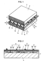
- FIG. 1 shows a perspective view illustrating a structure of PDP 1 manufactured with a method in accordance with the embodiment of the present invention.
- PDP 1 is formed of front panel 2 including front glass substrate 3, and rear panel 10 including rear glass substrate 11. Front panel 2 and rear panel 10 confront each other and the peripheries thereof are airtightly sealed with sealing agent such as glass frit, thereby forming discharge space 16, which is filled with discharge gas of Ne and Xe at a pressure falling within a range between 53.3 kPa and 80.0 kPa.
- dielectric layer 8 working as a capacitor is formed on front glass substrate 3 such that layer 8 can cover display electrodes 6 and lightproof layer 7.
- protective layer 9 made of magnesium oxide (MgO) is formed on the surface of dielectric layer 8.
- Multiple belt-like address electrodes 12 are placed in parallel with one another on rear glass substrate 11 of rear panel 10, and they are placed along a direction intersecting at right angles with scan electrodes 4 and sustain electrodes 5 formed on front panel 2.
- Primary dielectric layer 13 covers those address electrodes 12.
- Barrier ribs 14 having a given height are formed on primary dielectric layer 13 placed between respective address electrodes 12, and ribs 14 partition discharge space 16.
- Phosphor layers 15 are applied onto grooves formed between each one of barrier ribs 14 sequentially in response to respective address electrodes 12.
- Phosphor layers 15 emit light in red, blue, and green with an ultraviolet ray respectively.
- a discharge cell is formed at a junction point where scan electrode 4, sustain electrode 5 and address electrode 12 intersect with one another.
- the discharge cells having phosphor layers 15 of red, blue, and green respectively are placed along display electrodes 6, and these cells work as pixels for color display.
- Fig. 2 shows a sectional view illustrating a structure of front panel 2 of PDP1 in accordance with this embodiment.
- Fig. 2 shows front panel 2 upside down from that shown in Fig. 1 .
- display electrode 6 formed of scan electrode 4 and sustain electrode 5 is patterned on front glass substrate 3 manufactured by the float method.
- Lightproof layer 7 is also patterned together with display electrode 6 on substrate 3.
- Scan electrode 4 is formed of transparent electrodes 4a, 5a made of indium tin oxide (ITO) or tin oxide (SnO 2 ),and sustain electrode 5 is formed of metal bus electrodes 4b, 5b formed on transparent electrodes 4a, 5a.
- Metal bus electrodes 4b, 5b give electrical conductivity to transparent electrodes 4a, 5a along the longitudinal direction of electrodes 4a, 5a, and they are made of conductive material of which chief ingredient is silver (Ag).
- Dielectric layer 8 is formed of at least two layers, i.e. first dielectric layer 81 that covers transparent electrodes 4a, 5a and metal bus electrodes 4b, 5b and light proof layer 7 formed on front glass substrate 3, and second dielectric layer 82 formed on first dielectric layer 81.
- protective layer 9 of the PDP in accordance with this embodiment is formed this way: Primary film 91, made of magnesium oxide (MgO) or MgO containing aluminum (Al), is formed on dielectric layer 8, and aggregated particles 92 are dispersed discretely and almost uniformly on the entire surface of this primary film 91. Aggregated particle 92 is formed by aggregating multiple crystal particles made of metal oxide, i.e. MgO. The coverage with particles 92 over the surface of primary film 91 falls within the range from 2% to 12%.
- MgO magnesium oxide
- Al aluminum
- Coverage % a / b ⁇ 100 where "a” represents an area where aggregated particles 92 are attached within one discharge cell, and "b” represents an area of one discharge cell.
- a method for manufacturing the PDP is demonstrated hereinafter.
- Scan electrode 4 and sustain electrode 5 are respectively formed of transparent electrodes 4a, 5a and metal bus electrodes 4b, 5b. These transparent electrodes 4a, 5a, and metal bus electrodes 4b, 5b are patterned with a photo-lithography method.
- Transparent electrodes 4a, 5a are formed by using a thin-film process, and metal bus electrodes 4b, 5b are made by firing the paste containing silver (Ag) at a given temperature before the paste is hardened.
- Black stripes (lightproof layer) 7 is made by screen-printing the paste containing black pigment, or by forming the black pigment on the entire surface of the glass substrate, and then patterning the pigment with the photolithography method before the paste is fired.
- the dielectric paste is a kind of paint containing binder, solvent, and dielectric material such as glass powder.
- form protective layer 9 made of magnesium oxide (MgO) on dielectric layer 8 with the vacuum deposition method.
- the foregoing steps allow forming predetermined structural elements (display electrodes 6, lightproof layer 7, dielectric layer 8 and primary film 91), except aggregated particle 92, on front glass substrate 3.
- step A1 is done for forming dielectric layer 8
- step A2 is done for depositing primary film 91 chiefly made of MgO on dielectric layer 8 with the vacuum deposition method by using sintered body of MgO containing some aluminum (Al).
- step A3 attach discretely multiple aggregated particles 92 onto primary film 91 (step A3), which is formed in step A2 for depositing the primary film but is not yet fired.
- Particle 92 is to be metal oxide particles and is formed by aggregating crystal particles of MgO.
- this step A3 prepare the paste by mixing aggregated particles 92 with organic resin component into diluting agent, and then, apply this paste onto non-fired primary film 91 with a screen printing method for forming the metal oxide film.
- the metal oxide paste is detailed later.
- a spraying method, spin-coating method, die-coating method, or slit-coating method can be used for painting this paste on non-fired primary film 91 to form the paste film.
- step A4 The metal oxide paste film undergoes drying step A4. Then non-fired primary film 91 formed in step A2 and the paste film having undergone drying step A4 are fired together at several hundreds °C in firing step A5. In step A5, solvent and resin component remaining in the paste film are removed, so that protective layer 9, of which primary film 91 is attached with multiple aggregated particles 92, is completed.
- Step A3 for forming the film of metal oxide paste, step A4 for drying, and step A5 for firing are the steps for forming the particles of the metal oxide.
- primary film 91 chiefly made of MgO is used; however, according to the present invention, film 91 must withstand intensive sputtering because it should protect dielectric layer 9 from ion-impact, so that it is not necessarily to have high electron emission capability.
- a conventional PDP employs a protective layer formed of a primary film chiefly made of MgO in order to satisfy both of the electron emission performance and withstanding performance to the sputtering at a certain level or higher than the certain level.
- the PDP of the present invention employs the primary film attached with crystal particles of metal oxide onto the film, and crystal particles of the metal oxide dominantly control the electron emission performance.
- Primary film 91 therefore, is not necessarily made of MgO, but other materials more excellent in resistance to sputtering, such as Al 2 O 3 , can replace MgO.
- MgO particles are used as crystal particles of metal oxide; however, other crystal particles of metal oxide such as strontium (Sr), calcium (Ca), barium (Ba), and aluminum (Al) can replace MgO as long as they have the electron emission performance as high as MgO. Use of these metal oxides can also achieve similar advantages to the foregoing ones.
- a material of crystal particle is thus not limited only to MgO.
- the steps discussed above allow forming such structural elements on front glass substrate 3 as display electrodes 6, black stripes (lightproof layer) 7, dielectric layer 8, primary film 91, and aggregated particles 92 made of MgO.
- Rear panel 10 is formed this way: First, form a material layer, which is a structural element of address electrode 12, by screen-printing the paste containing silver (Ag) onto rear glass substrate 11, or by patterning with the photolithography method a metal film which is formed in advance on the entire surface of rear glass substrate 11. Then fire this material layer at a given temperature, thereby forming address electrodes 12. Next, form a dielectric paste layer (not shown) on rear glass substrate 11, on which address electrodes 12 are formed, by painting dielectric paste onto substrate 11 with the die-coating method such that the dielectric paste layer can cover address electrodes 12. Then fire the dielectric paste layer for forming primary dielectric layer 13.
- the dielectric paste is a kind of paint containing binder, solvent, and dielectric material such as glass powder.
- Front panel 2 and rear panel 10 discussed above are placed opposite to each other such that display electrodes 6 intersect at right angles with address electrodes 12, and the peripheries of panel 2 and panel 10 are sealed with glass frit to form discharge space 16 between panels 2 and 10, and space 16 is filled with discharge gas including Ne, Xe. PDP 1 is thus completed.
- the paste of metal oxide used for forming a layer attached with crystal particles of the metal oxide onto primary film 91, is detailed hereinafter.
- This layer is formed on primary film 91 in step A3 for forming the paste film of the metal oxide of the PDP manufactured with the method of the present invention.
- the description focuses on the experiment on ascertaining the advantage of volume and stable production of the paste.
- various chemicals are used; however, they and their numerical conditions such as amounts are examples within the scope of the present invention, so that the present invention is not limited to these examples.
- compositions listed in tables 1 and 2 are blended with a three-roll mill.
- the coverage with aggregated particles 92 made of MgO over primary film 91 preferably falls within the range from 2% to 12%. Since the coverage is determined by a thickness of the film of metal-oxide paste, the content of aggregated particles 92 made of MgO in the metal oxide paste preferably falls within the range from 0.01 vol% to 1.5 vol% based on the film thickness printable with the screen printing method.
- TABLE 1 Composition No. 101 102 103 104 105 106 107 108 109 110 111 Metal oxide MgO particle 0.20 0.20 0.20 0.20 0.20 0.20 0.20 0.20 0.20 0.20 0.20 0.20 0.20 0.20 0.20 0.20 Organic resin component Ethyl-cellulose 4cP 7.21 8.64 9.96 14.76 17.09 22.11 - - - - - Ethyl-cellulose 10cP - - - - - 7.21 8.64 9.46 12.47 15.16 Diluting agent Butyl carbitol 68.93 67.86 66.88 63.31 61.57 57.84 68.93 67.86 67.25 65.01 63.01 Terpinol 23.66 23.30 22.96 21.73 21.14 19.85 23.66 23.30 23.09 22.32 21.63 Total 100.00 100.00 100.00 100.00 100.00 100.00 100.00 100.00 100.00 100.00 100.00 TABLE 2 Composition
- composition Nos. 101 - 111 listed in table 1 show the viscosity (cP) of 4cP and 10cP due to difference in molecular weight grade of ethyl-cellulose, and composition Nos. 112 - 122 show the viscosity (cP) of 100cP and 200cP due to difference in molecular weight grade of ethyl-cellulose.
- the organic resin components listed in tables 1 and 2 employ ethyl-cellulose; however, cellulose derivatives other than ethyl-cellulose such as hydroxypropyl cellulose, hydroxyethyl cellulose, hydroxypropyl methylcellulose phtalate, hydroxypropyl methylcellulose acetate can be employed.
- the chemical compounds listed below can be also used: acrylic acid, methacrylic acid, methyl acrylate, methyl methacrylate, ethyl acrylate, ethyl methacrylate, butyl acrylate, butyl methacrylate, isobutyl acrylate, isobutyl methacrylate, mono-methyl fumarate, mono-ethyl fumarate, mono-propyl fumarate, mono-methyl maleate, mono-ethyl maleate, mono-propyl maleate, sorbic acid, hydroxymethyl acrylate, 2-hydroxyethyl acrylate, 2-hydroxymethyl methacrylate, 2-hydroxypropyl methacrylate, hydroxyl mono-acrylate, hydroxy mono-methacrylate, diacrylate hydroquinone, hydroquinone 2-dihydroxyl ethyl acrylate, 2-hydroxyethyl methacrylate, N-butyl acrylate, N-butylmethacrylate,
- Acrylate or methacrylate of the foregoing chemical compounds can be replaced with fumaric acid, i.e. fumarate, replaced with maleic acid, i.e. maleate, replaced with crotonic acie, i.e. crotonate, or replaced with itaconic acid, i.e. itaconate, or polymer or copolymer such as urethane methacrylate, styrene, acrylamide, methacrylamide, acrylonitrile, methacrylonitrile.
- Acrylic resin can be used alone, or can be combined with cellulose derivatives.
- diethylene glycol monobutyl ether (butyl carbitol) and terpinol are used as diluting agent; however, other chemicals as follows can be used alone, or two or more than two chemicals below can be combined together for replacing butyl carbitol and terpinol: ethylene glycol mono-methyl ether, ethylene glycol mono-ethyl ether, propylene glycol mono-methyl ether, propylene glycol mono-ethyl ether, diethylene glycol mono-methyl ether, diethylene glycol mono-ethyl ether, diethylene glycol dimethyl ether, diethylene glycol diethyl ether, propylene glycol mono-methyl ether acetate, propylene glycol mono-ethyl ether acetate, 2-methoxybutyl acetate, 3-methoxybutyl acetate, 4-methoxybutyl acetate, 2-methyl-3-methoxybutyl acetate, 3-methyl-3-methoxybutyl acetate
- the paste can contain, upon necessity, plasticizer such as dioctyl phthalate, dibutyl phthalate, triphenyl phosphate, tributyl phosphate, and dispersant such as glycerop mono-oleate, sorbitan sesquio-leate, homogenol (a product manufactured by Kao Corporation), alkyl-allyl based phosphate.
- plasticizer such as dioctyl phthalate, dibutyl phthalate, triphenyl phosphate, tributyl phosphate, and dispersant such as glycerop mono-oleate, sorbitan sesquio-leate, homogenol (a product manufactured by Kao Corporation), alkyl-allyl based phosphate.
- the metal oxide pastes each of which is formed of composition No. 101 - 122 respectively are painted on front glass substrate 3,where display electrodes 6, black stripes (lightproof layer) 7, dielectric layer 8, and primary film 91 are formed, with the screen printing method in order to test the respective pastes for printability.
- the screen printing employs L380S mesh as a screen.
- Fig. 4 shows the test result, namely, the characteristics of the metal oxide pastes employed in the method for manufacturing the PDP in accordance with the embodiment of the present invention.
- the test for the printability is done through eye observation to find knocking during the printing.
- a paste accompanied by knocking is marked in black, and a paste free from knocking is marked in white.
- the knocking in this context refers to "bit-by-bit vertical motion" of a squeegee on the mesh. The squeegee should move on the mesh smooth, but in this case, it somehow scratches on the mesh and vibrates vertically.
- Fig. 4 also shows viscosities (cP), differing in molecular weight grades of the ethyl-cellulose, as parameters. As Fig. 4 explicitly depicts, when the content of ethyl-cellulose contained in the metal oxide paste is less than 8 vol%, knocking is observed regardless of the viscosity depending on the molecular weight grades.
- the coverage with aggregated particles 92 over front glass substrate 3 accompanied by the knocking is measured to find a dispersion of over 10% within an area, while a coverage over substrate 3 free from the knocking measures as good as not greater than 6% within the area.
- step A5 the organic resin component contained in the metal oxide paste is removed in firing step A5 after step A3 (forming the paste film) and drying step A4.
- step A5 a greater amount of the organic resin component contained in the paste will increase an amount of residual after the firing.
- a completed PDP still carries some residual, which adversely affects the discharge characteristics.
- the metal oxide paste having the following structure allows manufacturing PDPs excellent in printability and free from degradation in the discharge characteristics caused by the residual of the organic resin component after the firing:
- the metal oxide paste is formed of the metal oxide particles, the organic resin component, and the diluting agent, and the paste contains the metal oxide particles not greater than 1.5 vol% and the organic resin component falling within the range from 8.0 to 20.0 vol%.
- PDP 1 is produced with the method for manufacturing PDPs in accordance with the embodiment of the present invention.
- Sample 1 is a PDP of which protective layer 9 is formed of the film made of only MgO.
- Sample 2 is a PDP of which protective layer 9 is formed of MgO into which impurity such as aluminum (Al) or silicon (Si) is doped.
- Sample 3 is PDP 1 in accordance with the embodiment of the present invention.
- This PDP 1, i.e. sample 3 includes protective layer 9 having primary film 91 made of MgO, and aggregated particles 92, formed by aggregating multiple crystal particles of metal oxide, are uniformly distributed and attached on the entire surface of film 91. Cathode luminescence of the single crystal particle employed in sample 3 is measured to find the characteristics as shown in Fig. 5 .
- the electron emission performance is a numerical value, i.e. a greater value indicates a greater amount of electron emitted, and is expressed with an amount of primary electron emitted, which is determined by a surface condition and a type of gas.
- the amount of primary electron emitted can be measured with a method that is used for measuring an amount of electron-current emitted from the surface of protective layer 9 through irradiating the surface with ions or an electron beam.
- the evaluation method disclosed in Unexamined Japanese Patent Publication No. 2007 - 48733 is thus employed to measure a discharge delay ("ts" value) as the electron emission performance.
- a statistical delay time which is a reference to the easiness of discharge occurrence, among delay times in discharge is measured.
- This reference number is inversed, and then integrated, thereby obtaining a value which linearly corresponds to the amount of emitted primary electrons, so that the value is used for the test.
- the delay time in discharge expresses the time of discharge delay (hereinafter referred to as "ts" value) from the pulse rising, and the discharge delay is chiefly caused by the struggle of the initial electrons, which trigger off the discharge, for emitting from the surface of the protective layer into the discharge space.
- the electric charge retention performance is expressed with a voltage value applied to scan electrodes (hereinafter referred to as a "Vscn" lighting voltage), which is needed for suppressing an electron emission phenomenon of PDP1.
- Vscn a voltage value applied to scan electrodes
- higher electric charge retention performance can be expected at a lower Vscn lighting voltage, so that a lower Vscn voltage allows the PDP to be driven at a lower voltage design-wise.
- the power supply and electric components with a smaller withstanding voltage and a smaller capacity can be employed.
- semiconductor switching elements such as MOSFET are used for applying a scan voltage sequentially, and these switching elements have approx. 150V as a withstanding voltage.
- the Vscn lighting voltage is thus preferably lowered to not greater than 120V in the environment of 70°C taking it into consideration that some change can occur due to variation caused by temperature.
- Fig. 6 shows the relation between the electron emission performance and the electric charge retention performance.
- the horizontal axis of Fig. 6 represents the electron emission performance, and the test result of sample 1 is shown as a reference value.
- sample 3 can achieve controlling the Vscn lighting voltage to be not greater than 120V in the electric charge retention test, and yet, it can achieve approx. six times or more as good as sample 1 in the electron emission performance.
- Sample 3 includes, as described previously, aggregated particles 92 each of which is formed by aggregating multiple crystal particles of MgO, and particles 92 are uniformly distributed on the surface of primary film 91 made of MgO.
- protective layer 9 of PDP 1 conflict with each other. For instance, a change in film-forming condition of protective layer 9, or doping an impurity such as Al, Si, or Ba into protective layer 9 of sample 2 during the film-forming process, will improve the electron emission performance; however, the change or the doping will raise the Vscn lighting voltage as a side effect.
- the present invention allows obtaining protective layer 9 which can satisfy both of the electron emission capability and the electric charge retention capability appropriate to the PDP which is required to display an increased number of scanning lines as well as to have the smaller size cells due to the advent of high definition display.
- the particle diameter refers to an average particle diameter, which means a volume cumulative average diameter (D50).
- Fig. 7 shows a test result of sample 3 described in Fig. 6 , and the test is done for the electron emission performance by changing a particle diameter of the crystal particle of MgO.
- the diameter of the crystal particle of MgO shows an average diameter measured with the micro-track HRA particle-size distribution meter in ethanol solution of the first grade reagent defined by JIS or the higher grade of the reagent, and the crystal particle is observed in SEM photo to be measured.
- the particle diameter as small as 0.3 ⁇ m results in the lower electron emission performance, while the particle diameter as great as 0.9 ⁇ m or more results in the higher electron emission performance.
- a greater number of crystal particles per unit area on protective layer 9 is preferable for increasing the number of emitted electrons within a discharge cell.
- the experiment teaches the inventors the following fact: presence of the crystal particles at the top of barrier rib 14, with which protective layer 9 of front panel 2 closely contacts, breaks the top of barrier rib 14, and then the material of rib 14 falls on phosphor layer 15, so that the cell encountering this problem cannot normally go on or go out.
- This breakage in the barrier ribs resists occurring when the crystal particles do not exist at the top of barrier rib 14, so that a greater number of the crystal particles will increase the occurrence of breakage in barrier ribs 14.
- Fig. 8 shows relations between the particle diameter of the crystal particle and the breakage in barrier rib 14.
- the same numbers of the crystal particles per unit area although they have different diameters are sprayed in sample 3.
- the probability of breakage in barrier ribs 14 sharply increases when the diameter of the crystal particle becomes as large as 2.5 ⁇ m; however, it stays at a rather low level when the diameter stays not greater than 2.5 ⁇ m.
- aggregated particle 92 preferably has a particle diameter within a range from 0.9 ⁇ m to 2.5 ⁇ m. However, it is necessary to consider a dispersion of crystal particles in manufacturing and a dispersion of protective layers 9 in manufacturing.
- Fig. 9 shows an instance of particle size distribution of aggregated particle 92 employed in PDP1 of the present invention.
- Aggregated particle 92 has the particle size distribution as shown in Fig. 9 , and the electron emission characteristics shown in Fig. 7 and barrier-rib breakage characteristics shown in Fig. 8 teach that it is preferable to use the aggregated particles, of which average particle diameter, i.e. volume cumulative average diameter (D50), falls within a range from 0.9 ⁇ m to 2 ⁇ m.
- average particle diameter i.e. volume cumulative average diameter (D50)
- PDP 1 having protective layer 9 formed of metal oxide in accordance with this embodiment achieves electron emission capability more than six times as good as the protective layer formed of the primary film made of only MgO, and also achieves the electric charge retention capability such as the Vscn lighting voltage not greater than 120V.
- PDP1 thus can satisfy both of the electron emission capability and the electric charge retention capability, although PDP1 is to display an increased number of scanning lines as well as to have the smaller size cells due to the advent of high definition display..
- the PDP which can display a high definition video at high luminance with lower power consumption, is thus obtainable.
- aggregated particles 92 formed of crystal particles of MgO are distributed and attached onto the entire surface of primary film 91 with the coverage ranging from 2% to 12%.
- This coverage range derives from the experiments for characteristics of the samples each of which coverage with aggregated particles 92 over primary film 91 differs from one another.
- the experiments prove that the Vscn lighting voltage rises at a greater coverage with aggregated particles 92, so that the electric charge retention capability degrades. To the contrary, the Vscn lighting voltage lowers at a smaller coverage.
- the experiments teach the inventors that the coverage not greater than 12% can take full advantage of aggregated particles 92 attached onto the surface of primary film 91.
- Aggregated particles 92 of MgO are needed in each one of the discharge cells for reducing the dispersion of the characteristics. Aggregated particles 92 should be thus attached on the surface of primary film 91. A smaller coverage with particles 92 thus tends to increase the dispersion on the surface, and an amount of particles 92 attached to each discharge cell differs greatly between the cells.
- the experiments also teach the inventors that the attachment of particles 92 formed of crystal particles of MgO at the coverage of 4% or more allows reducing the dispersion to approx. not greater than 4%, and the attachment of particles 92 at the coverage of 2% or more allows reducing the dispersion to approx. at 6%, which causes practically no problem.
- aggregated particles 92 formed of crystal particles of MgO are preferably attached to primary film 91 at the coverage ranging from 2% to 12%, and more preferably, the coverage ranges from 4% to 12%.
- the present invention is useful for providing a PDP capable of displaying high definition at high luminance with lower power consumption.
Landscapes
- Engineering & Computer Science (AREA)
- Physics & Mathematics (AREA)
- Plasma & Fusion (AREA)
- Manufacturing & Machinery (AREA)
- Gas-Filled Discharge Tubes (AREA)
Claims (3)
- Verfahren zum Herstellen einer Plasmaanzeigetafel, die folgendes umfasst:eine vordere Tafel, die eine dielektrische Schicht zum Abdecken von Anzeigeelektroden, welche auf einem Substrat ausgebildet sind, und eine Schutzschicht enthält, die auf der dielektrischen Schicht ausgebildet ist; undeine hintere Tafel, die der vorderen Tafel zum Ausbilden eines Entladungsraums zwischen der vorderen Tafel und der hinteren Tafel gegenüberliegt und Adresselektroden entlang einer Richtung, die die Anzeigeelektroden schneidet, und Grenzrippen zum Aufteilen des Entladungsraums enthält,das Verfahren folgenden Schritt umfassend:Ausbilden der Schutzschicht der vorderen Tafel, und wobei dieser Schritt folgende Schritte enthält:Ausbilden eines primären Films durch Abscheiden des primären Films auf der dielektrischen Schicht; undAusbilden von Metalloxidpartikeln durch Aufstreichen von Metalloxidpaste, die die Metalloxidpartikeln, organische Harzkomponente und Verdünnungsmittel enthält, auf den primären Film und anschließendes Brennen der Metalloxidpaste zum Aufbringen von mehreren der Metalloxidpartikeln auf den primären Film,wobei die Metalloxidpaste die Metalloxidpartikeln nicht über 1,5% Volumengehalt und die organische Harzkomponente innerhalb eines Bereichs von 8,0 bis 20,0% Volumengehalt enthält.
- Verfahren nach Anspruch 1, wobei die Metalloxidpaste die Metalloxidpartikeln nicht unter 0,01% Volumengehalt enthält.
- Verfahren nach Anspruch 1, wobei die Metalloxidpartikeln mit einem Filmdruckverfahren aufgestrichen werden.
Applications Claiming Priority (2)
| Application Number | Priority Date | Filing Date | Title |
|---|---|---|---|
| JP2008101196A JP5012630B2 (ja) | 2008-04-09 | 2008-04-09 | プラズマディスプレイパネル用金属酸化物ペースト及びプラズマディスプレイパネルの製造方法 |
| PCT/JP2009/001585 WO2009125570A1 (ja) | 2008-04-09 | 2009-04-06 | プラズマディスプレイパネルの製造方法 |
Publications (3)
| Publication Number | Publication Date |
|---|---|
| EP2146365A1 EP2146365A1 (de) | 2010-01-20 |
| EP2146365A4 EP2146365A4 (de) | 2011-07-27 |
| EP2146365B1 true EP2146365B1 (de) | 2012-07-11 |
Family
ID=41161707
Family Applications (1)
| Application Number | Title | Priority Date | Filing Date |
|---|---|---|---|
| EP09716191A Not-in-force EP2146365B1 (de) | 2008-04-09 | 2009-04-06 | Verfahren zur herstellung einer plasmaanzeigetafel |
Country Status (5)
| Country | Link |
|---|---|
| EP (1) | EP2146365B1 (de) |
| JP (1) | JP5012630B2 (de) |
| KR (1) | KR101027607B1 (de) |
| CN (1) | CN101681758B (de) |
| WO (1) | WO2009125570A1 (de) |
Families Citing this family (1)
| Publication number | Priority date | Publication date | Assignee | Title |
|---|---|---|---|---|
| WO2023054769A1 (ko) | 2021-10-01 | 2023-04-06 | 엘지전자 주식회사 | 디스플레이 제조 장치 |
Family Cites Families (6)
| Publication number | Priority date | Publication date | Assignee | Title |
|---|---|---|---|---|
| JPH0912940A (ja) * | 1995-07-04 | 1997-01-14 | Oki Electric Ind Co Ltd | 誘電体保護膜形成用ペースト |
| JP4399344B2 (ja) * | 2004-11-22 | 2010-01-13 | パナソニック株式会社 | プラズマディスプレイパネルおよびその製造方法 |
| EP1780749A3 (de) * | 2005-11-01 | 2009-08-12 | LG Electronics Inc. | Plasmaanzeigetafel und Herstellungsverfahren |
| JP2007149384A (ja) * | 2005-11-24 | 2007-06-14 | Pioneer Electronic Corp | プラズマディスプレイパネルの製造方法、および、プラズマディスプレイパネル |
| JP4148982B2 (ja) * | 2006-05-31 | 2008-09-10 | 松下電器産業株式会社 | プラズマディスプレイパネル |
| EP1883092A3 (de) * | 2006-07-28 | 2009-08-05 | LG Electronics Inc. | Plasmaanzeigetafel und Verfahren zu ihrer Herstellung |
-
2008
- 2008-04-09 JP JP2008101196A patent/JP5012630B2/ja not_active Expired - Fee Related
-
2009
- 2009-04-06 KR KR1020097020467A patent/KR101027607B1/ko not_active Expired - Fee Related
- 2009-04-06 CN CN200980000288XA patent/CN101681758B/zh not_active Expired - Fee Related
- 2009-04-06 WO PCT/JP2009/001585 patent/WO2009125570A1/ja not_active Ceased
- 2009-04-06 EP EP09716191A patent/EP2146365B1/de not_active Not-in-force
Also Published As
| Publication number | Publication date |
|---|---|
| JP5012630B2 (ja) | 2012-08-29 |
| WO2009125570A1 (ja) | 2009-10-15 |
| EP2146365A4 (de) | 2011-07-27 |
| JP2009252621A (ja) | 2009-10-29 |
| CN101681758B (zh) | 2012-04-04 |
| KR20090122367A (ko) | 2009-11-27 |
| EP2146365A1 (de) | 2010-01-20 |
| CN101681758A (zh) | 2010-03-24 |
| KR101027607B1 (ko) | 2011-04-06 |
Similar Documents
| Publication | Publication Date | Title |
|---|---|---|
| US8120254B2 (en) | Plasma display panel comprising sputtering prevention layer | |
| EP2146366A1 (de) | Plasmaanzeigetafel | |
| US20100203792A1 (en) | Method for manufacturing plasma display panel | |
| EP2136384A1 (de) | Verfahren zur herstellung einer plasmaanzeigetafel | |
| EP2146365B1 (de) | Verfahren zur herstellung einer plasmaanzeigetafel | |
| US20100130088A1 (en) | Method for manufacturing plasma display panel | |
| EP2187422B1 (de) | Verfahren zur herstellung einer plasmaanzeigetafel | |
| US8198813B2 (en) | Plasma display panel | |
| US8051549B2 (en) | Method for producing plasma display panel | |
| EP2141726B1 (de) | Plasmaanzeigetafel | |
| JP2010015697A (ja) | プラズマディスプレイパネル用金属酸化物ペースト及びプラズマディスプレイパネルの製造方法 | |
| EP2128884A1 (de) | Plasmaanzeigetafel |
Legal Events
| Date | Code | Title | Description |
|---|---|---|---|
| PUAI | Public reference made under article 153(3) epc to a published international application that has entered the european phase |
Free format text: ORIGINAL CODE: 0009012 |
|
| 17P | Request for examination filed |
Effective date: 20090904 |
|
| AK | Designated contracting states |
Kind code of ref document: A1 Designated state(s): AT BE BG CH CY CZ DE DK EE ES FI FR GB GR HR HU IE IS IT LI LT LU LV MC MK MT NL NO PL PT RO SE SI SK TR |
|
| AX | Request for extension of the european patent |
Extension state: AL BA RS |
|
| DAX | Request for extension of the european patent (deleted) | ||
| A4 | Supplementary search report drawn up and despatched |
Effective date: 20110629 |
|
| GRAP | Despatch of communication of intention to grant a patent |
Free format text: ORIGINAL CODE: EPIDOSNIGR1 |
|
| RIC1 | Information provided on ipc code assigned before grant |
Ipc: H01J 11/38 20120101ALI20120201BHEP Ipc: H01J 9/02 20060101AFI20120201BHEP |
|
| GRAS | Grant fee paid |
Free format text: ORIGINAL CODE: EPIDOSNIGR3 |
|
| GRAA | (expected) grant |
Free format text: ORIGINAL CODE: 0009210 |
|
| AK | Designated contracting states |
Kind code of ref document: B1 Designated state(s): AT BE BG CH CY CZ DE DK EE ES FI FR GB GR HR HU IE IS IT LI LT LU LV MC MK MT NL NO PL PT RO SE SI SK TR |
|
| REG | Reference to a national code |
Ref country code: GB Ref legal event code: FG4D |
|
| REG | Reference to a national code |
Ref country code: CH Ref legal event code: EP |
|
| REG | Reference to a national code |
Ref country code: AT Ref legal event code: REF Ref document number: 566495 Country of ref document: AT Kind code of ref document: T Effective date: 20120715 |
|
| REG | Reference to a national code |
Ref country code: IE Ref legal event code: FG4D |
|
| REG | Reference to a national code |
Ref country code: DE Ref legal event code: R096 Ref document number: 602009008216 Country of ref document: DE Effective date: 20120906 |
|
| REG | Reference to a national code |
Ref country code: NL Ref legal event code: VDEP Effective date: 20120711 |
|
| REG | Reference to a national code |
Ref country code: AT Ref legal event code: MK05 Ref document number: 566495 Country of ref document: AT Kind code of ref document: T Effective date: 20120711 |
|
| REG | Reference to a national code |
Ref country code: LT Ref legal event code: MG4D Effective date: 20120711 |
|
| PG25 | Lapsed in a contracting state [announced via postgrant information from national office to epo] |
Ref country code: AT Free format text: LAPSE BECAUSE OF FAILURE TO SUBMIT A TRANSLATION OF THE DESCRIPTION OR TO PAY THE FEE WITHIN THE PRESCRIBED TIME-LIMIT Effective date: 20120711 Ref country code: FI Free format text: LAPSE BECAUSE OF FAILURE TO SUBMIT A TRANSLATION OF THE DESCRIPTION OR TO PAY THE FEE WITHIN THE PRESCRIBED TIME-LIMIT Effective date: 20120711 Ref country code: BE Free format text: LAPSE BECAUSE OF FAILURE TO SUBMIT A TRANSLATION OF THE DESCRIPTION OR TO PAY THE FEE WITHIN THE PRESCRIBED TIME-LIMIT Effective date: 20120711 Ref country code: HR Free format text: LAPSE BECAUSE OF FAILURE TO SUBMIT A TRANSLATION OF THE DESCRIPTION OR TO PAY THE FEE WITHIN THE PRESCRIBED TIME-LIMIT Effective date: 20120711 Ref country code: LT Free format text: LAPSE BECAUSE OF FAILURE TO SUBMIT A TRANSLATION OF THE DESCRIPTION OR TO PAY THE FEE WITHIN THE PRESCRIBED TIME-LIMIT Effective date: 20120711 Ref country code: CY Free format text: LAPSE BECAUSE OF FAILURE TO SUBMIT A TRANSLATION OF THE DESCRIPTION OR TO PAY THE FEE WITHIN THE PRESCRIBED TIME-LIMIT Effective date: 20120711 Ref country code: NO Free format text: LAPSE BECAUSE OF FAILURE TO SUBMIT A TRANSLATION OF THE DESCRIPTION OR TO PAY THE FEE WITHIN THE PRESCRIBED TIME-LIMIT Effective date: 20121011 Ref country code: IS Free format text: LAPSE BECAUSE OF FAILURE TO SUBMIT A TRANSLATION OF THE DESCRIPTION OR TO PAY THE FEE WITHIN THE PRESCRIBED TIME-LIMIT Effective date: 20121111 |
|
| PG25 | Lapsed in a contracting state [announced via postgrant information from national office to epo] |
Ref country code: PL Free format text: LAPSE BECAUSE OF FAILURE TO SUBMIT A TRANSLATION OF THE DESCRIPTION OR TO PAY THE FEE WITHIN THE PRESCRIBED TIME-LIMIT Effective date: 20120711 Ref country code: GR Free format text: LAPSE BECAUSE OF FAILURE TO SUBMIT A TRANSLATION OF THE DESCRIPTION OR TO PAY THE FEE WITHIN THE PRESCRIBED TIME-LIMIT Effective date: 20121012 Ref country code: PT Free format text: LAPSE BECAUSE OF FAILURE TO SUBMIT A TRANSLATION OF THE DESCRIPTION OR TO PAY THE FEE WITHIN THE PRESCRIBED TIME-LIMIT Effective date: 20121112 Ref country code: SI Free format text: LAPSE BECAUSE OF FAILURE TO SUBMIT A TRANSLATION OF THE DESCRIPTION OR TO PAY THE FEE WITHIN THE PRESCRIBED TIME-LIMIT Effective date: 20120711 Ref country code: LV Free format text: LAPSE BECAUSE OF FAILURE TO SUBMIT A TRANSLATION OF THE DESCRIPTION OR TO PAY THE FEE WITHIN THE PRESCRIBED TIME-LIMIT Effective date: 20120711 Ref country code: SE Free format text: LAPSE BECAUSE OF FAILURE TO SUBMIT A TRANSLATION OF THE DESCRIPTION OR TO PAY THE FEE WITHIN THE PRESCRIBED TIME-LIMIT Effective date: 20120711 |
|
| PG25 | Lapsed in a contracting state [announced via postgrant information from national office to epo] |
Ref country code: NL Free format text: LAPSE BECAUSE OF FAILURE TO SUBMIT A TRANSLATION OF THE DESCRIPTION OR TO PAY THE FEE WITHIN THE PRESCRIBED TIME-LIMIT Effective date: 20120711 |
|
| PG25 | Lapsed in a contracting state [announced via postgrant information from national office to epo] |
Ref country code: EE Free format text: LAPSE BECAUSE OF FAILURE TO SUBMIT A TRANSLATION OF THE DESCRIPTION OR TO PAY THE FEE WITHIN THE PRESCRIBED TIME-LIMIT Effective date: 20120711 Ref country code: CZ Free format text: LAPSE BECAUSE OF FAILURE TO SUBMIT A TRANSLATION OF THE DESCRIPTION OR TO PAY THE FEE WITHIN THE PRESCRIBED TIME-LIMIT Effective date: 20120711 Ref country code: ES Free format text: LAPSE BECAUSE OF FAILURE TO SUBMIT A TRANSLATION OF THE DESCRIPTION OR TO PAY THE FEE WITHIN THE PRESCRIBED TIME-LIMIT Effective date: 20121022 Ref country code: DK Free format text: LAPSE BECAUSE OF FAILURE TO SUBMIT A TRANSLATION OF THE DESCRIPTION OR TO PAY THE FEE WITHIN THE PRESCRIBED TIME-LIMIT Effective date: 20120711 Ref country code: RO Free format text: LAPSE BECAUSE OF FAILURE TO SUBMIT A TRANSLATION OF THE DESCRIPTION OR TO PAY THE FEE WITHIN THE PRESCRIBED TIME-LIMIT Effective date: 20120711 |
|
| PLBE | No opposition filed within time limit |
Free format text: ORIGINAL CODE: 0009261 |
|
| STAA | Information on the status of an ep patent application or granted ep patent |
Free format text: STATUS: NO OPPOSITION FILED WITHIN TIME LIMIT |
|
| PG25 | Lapsed in a contracting state [announced via postgrant information from national office to epo] |
Ref country code: IT Free format text: LAPSE BECAUSE OF FAILURE TO SUBMIT A TRANSLATION OF THE DESCRIPTION OR TO PAY THE FEE WITHIN THE PRESCRIBED TIME-LIMIT Effective date: 20120711 Ref country code: SK Free format text: LAPSE BECAUSE OF FAILURE TO SUBMIT A TRANSLATION OF THE DESCRIPTION OR TO PAY THE FEE WITHIN THE PRESCRIBED TIME-LIMIT Effective date: 20120711 |
|
| 26N | No opposition filed |
Effective date: 20130412 |
|
| PG25 | Lapsed in a contracting state [announced via postgrant information from national office to epo] |
Ref country code: BG Free format text: LAPSE BECAUSE OF FAILURE TO SUBMIT A TRANSLATION OF THE DESCRIPTION OR TO PAY THE FEE WITHIN THE PRESCRIBED TIME-LIMIT Effective date: 20121011 |
|
| REG | Reference to a national code |
Ref country code: DE Ref legal event code: R097 Ref document number: 602009008216 Country of ref document: DE Effective date: 20130412 |
|
| PG25 | Lapsed in a contracting state [announced via postgrant information from national office to epo] |
Ref country code: MC Free format text: LAPSE BECAUSE OF FAILURE TO SUBMIT A TRANSLATION OF THE DESCRIPTION OR TO PAY THE FEE WITHIN THE PRESCRIBED TIME-LIMIT Effective date: 20120711 |
|
| REG | Reference to a national code |
Ref country code: CH Ref legal event code: PL |
|
| GBPC | Gb: european patent ceased through non-payment of renewal fee |
Effective date: 20130406 |
|
| REG | Reference to a national code |
Ref country code: IE Ref legal event code: MM4A |
|
| PG25 | Lapsed in a contracting state [announced via postgrant information from national office to epo] |
Ref country code: LI Free format text: LAPSE BECAUSE OF NON-PAYMENT OF DUE FEES Effective date: 20130430 Ref country code: CH Free format text: LAPSE BECAUSE OF NON-PAYMENT OF DUE FEES Effective date: 20130430 Ref country code: DE Free format text: LAPSE BECAUSE OF NON-PAYMENT OF DUE FEES Effective date: 20131101 Ref country code: GB Free format text: LAPSE BECAUSE OF NON-PAYMENT OF DUE FEES Effective date: 20130406 |
|
| REG | Reference to a national code |
Ref country code: FR Ref legal event code: ST Effective date: 20131231 |
|
| REG | Reference to a national code |
Ref country code: DE Ref legal event code: R119 Ref document number: 602009008216 Country of ref document: DE Effective date: 20131101 |
|
| PG25 | Lapsed in a contracting state [announced via postgrant information from national office to epo] |
Ref country code: FR Free format text: LAPSE BECAUSE OF NON-PAYMENT OF DUE FEES Effective date: 20130430 |
|
| PG25 | Lapsed in a contracting state [announced via postgrant information from national office to epo] |
Ref country code: IE Free format text: LAPSE BECAUSE OF NON-PAYMENT OF DUE FEES Effective date: 20130406 |
|
| PG25 | Lapsed in a contracting state [announced via postgrant information from national office to epo] |
Ref country code: MT Free format text: LAPSE BECAUSE OF FAILURE TO SUBMIT A TRANSLATION OF THE DESCRIPTION OR TO PAY THE FEE WITHIN THE PRESCRIBED TIME-LIMIT Effective date: 20120711 |
|
| PG25 | Lapsed in a contracting state [announced via postgrant information from national office to epo] |
Ref country code: TR Free format text: LAPSE BECAUSE OF FAILURE TO SUBMIT A TRANSLATION OF THE DESCRIPTION OR TO PAY THE FEE WITHIN THE PRESCRIBED TIME-LIMIT Effective date: 20120711 |
|
| PG25 | Lapsed in a contracting state [announced via postgrant information from national office to epo] |
Ref country code: MK Free format text: LAPSE BECAUSE OF FAILURE TO SUBMIT A TRANSLATION OF THE DESCRIPTION OR TO PAY THE FEE WITHIN THE PRESCRIBED TIME-LIMIT Effective date: 20120711 Ref country code: LU Free format text: LAPSE BECAUSE OF NON-PAYMENT OF DUE FEES Effective date: 20130406 Ref country code: HU Free format text: LAPSE BECAUSE OF FAILURE TO SUBMIT A TRANSLATION OF THE DESCRIPTION OR TO PAY THE FEE WITHIN THE PRESCRIBED TIME-LIMIT; INVALID AB INITIO Effective date: 20090406 |