EP2146378A2 - Halbleitervorrichtung - Google Patents
Halbleitervorrichtung Download PDFInfo
- Publication number
- EP2146378A2 EP2146378A2 EP20090165584 EP09165584A EP2146378A2 EP 2146378 A2 EP2146378 A2 EP 2146378A2 EP 20090165584 EP20090165584 EP 20090165584 EP 09165584 A EP09165584 A EP 09165584A EP 2146378 A2 EP2146378 A2 EP 2146378A2
- Authority
- EP
- European Patent Office
- Prior art keywords
- active layer
- layer
- semiconductor device
- gate insulating
- active
- Prior art date
- Legal status (The legal status is an assumption and is not a legal conclusion. Google has not performed a legal analysis and makes no representation as to the accuracy of the status listed.)
- Granted
Links
Images





Classifications
-
- H—ELECTRICITY
- H10—SEMICONDUCTOR DEVICES; ELECTRIC SOLID-STATE DEVICES NOT OTHERWISE PROVIDED FOR
- H10D—INORGANIC ELECTRIC SEMICONDUCTOR DEVICES
- H10D62/00—Semiconductor bodies, or regions thereof, of devices having potential barriers
- H10D62/80—Semiconductor bodies, or regions thereof, of devices having potential barriers characterised by the materials
- H10D62/85—Semiconductor bodies, or regions thereof, of devices having potential barriers characterised by the materials being Group III-V materials, e.g. GaAs
- H10D62/8503—Nitride Group III-V materials, e.g. AlN or GaN
-
- H—ELECTRICITY
- H10—SEMICONDUCTOR DEVICES; ELECTRIC SOLID-STATE DEVICES NOT OTHERWISE PROVIDED FOR
- H10D—INORGANIC ELECTRIC SEMICONDUCTOR DEVICES
- H10D30/00—Field-effect transistors [FET]
- H10D30/40—FETs having zero-dimensional [0D], one-dimensional [1D] or two-dimensional [2D] charge carrier gas channels
- H10D30/47—FETs having zero-dimensional [0D], one-dimensional [1D] or two-dimensional [2D] charge carrier gas channels having two-dimensional [2D] charge carrier gas channels, e.g. nanoribbon FETs or high electron mobility transistors [HEMT]
-
- H—ELECTRICITY
- H10—SEMICONDUCTOR DEVICES; ELECTRIC SOLID-STATE DEVICES NOT OTHERWISE PROVIDED FOR
- H10D—INORGANIC ELECTRIC SEMICONDUCTOR DEVICES
- H10D30/00—Field-effect transistors [FET]
- H10D30/01—Manufacture or treatment
- H10D30/015—Manufacture or treatment of FETs having heterojunction interface channels or heterojunction gate electrodes, e.g. HEMT
-
- H—ELECTRICITY
- H10—SEMICONDUCTOR DEVICES; ELECTRIC SOLID-STATE DEVICES NOT OTHERWISE PROVIDED FOR
- H10D—INORGANIC ELECTRIC SEMICONDUCTOR DEVICES
- H10D30/00—Field-effect transistors [FET]
- H10D30/40—FETs having zero-dimensional [0D], one-dimensional [1D] or two-dimensional [2D] charge carrier gas channels
- H10D30/47—FETs having zero-dimensional [0D], one-dimensional [1D] or two-dimensional [2D] charge carrier gas channels having two-dimensional [2D] charge carrier gas channels, e.g. nanoribbon FETs or high electron mobility transistors [HEMT]
- H10D30/471—High electron mobility transistors [HEMT] or high hole mobility transistors [HHMT]
- H10D30/473—High electron mobility transistors [HEMT] or high hole mobility transistors [HHMT] having confinement of carriers by multiple heterojunctions, e.g. quantum well HEMT
- H10D30/4732—High electron mobility transistors [HEMT] or high hole mobility transistors [HHMT] having confinement of carriers by multiple heterojunctions, e.g. quantum well HEMT using Group III-V semiconductor material
-
- H—ELECTRICITY
- H10—SEMICONDUCTOR DEVICES; ELECTRIC SOLID-STATE DEVICES NOT OTHERWISE PROVIDED FOR
- H10D—INORGANIC ELECTRIC SEMICONDUCTOR DEVICES
- H10D30/00—Field-effect transistors [FET]
- H10D30/40—FETs having zero-dimensional [0D], one-dimensional [1D] or two-dimensional [2D] charge carrier gas channels
- H10D30/47—FETs having zero-dimensional [0D], one-dimensional [1D] or two-dimensional [2D] charge carrier gas channels having two-dimensional [2D] charge carrier gas channels, e.g. nanoribbon FETs or high electron mobility transistors [HEMT]
- H10D30/471—High electron mobility transistors [HEMT] or high hole mobility transistors [HHMT]
- H10D30/475—High electron mobility transistors [HEMT] or high hole mobility transistors [HHMT] having wider bandgap layer formed on top of lower bandgap active layer, e.g. undoped barrier HEMTs such as i-AlGaN/GaN HEMTs
- H10D30/4755—High electron mobility transistors [HEMT] or high hole mobility transistors [HHMT] having wider bandgap layer formed on top of lower bandgap active layer, e.g. undoped barrier HEMTs such as i-AlGaN/GaN HEMTs having wide bandgap charge-carrier supplying layers, e.g. modulation doped HEMTs such as n-AlGaAs/GaAs HEMTs
-
- H—ELECTRICITY
- H10—SEMICONDUCTOR DEVICES; ELECTRIC SOLID-STATE DEVICES NOT OTHERWISE PROVIDED FOR
- H10D—INORGANIC ELECTRIC SEMICONDUCTOR DEVICES
- H10D64/00—Electrodes of devices having potential barriers
- H10D64/01—Manufacture or treatment
- H10D64/013—Manufacture or treatment of electrodes having a conductor capacitively coupled to a semiconductor by an insulator
-
- H—ELECTRICITY
- H10—SEMICONDUCTOR DEVICES; ELECTRIC SOLID-STATE DEVICES NOT OTHERWISE PROVIDED FOR
- H10D—INORGANIC ELECTRIC SEMICONDUCTOR DEVICES
- H10D64/00—Electrodes of devices having potential barriers
- H10D64/20—Electrodes characterised by their shapes, relative sizes or dispositions
- H10D64/27—Electrodes not carrying the current to be rectified, amplified, oscillated or switched, e.g. gates
- H10D64/311—Gate electrodes for field-effect devices
- H10D64/411—Gate electrodes for field-effect devices for FETs
-
- H—ELECTRICITY
- H10—SEMICONDUCTOR DEVICES; ELECTRIC SOLID-STATE DEVICES NOT OTHERWISE PROVIDED FOR
- H10D—INORGANIC ELECTRIC SEMICONDUCTOR DEVICES
- H10D64/00—Electrodes of devices having potential barriers
- H10D64/20—Electrodes characterised by their shapes, relative sizes or dispositions
- H10D64/27—Electrodes not carrying the current to be rectified, amplified, oscillated or switched, e.g. gates
- H10D64/311—Gate electrodes for field-effect devices
- H10D64/411—Gate electrodes for field-effect devices for FETs
- H10D64/511—Gate electrodes for field-effect devices for FETs for IGFETs
- H10D64/512—Disposition of the gate electrodes, e.g. buried gates
- H10D64/513—Disposition of the gate electrodes, e.g. buried gates within recesses in the substrate, e.g. trench gates, groove gates or buried gates
-
- H—ELECTRICITY
- H10—SEMICONDUCTOR DEVICES; ELECTRIC SOLID-STATE DEVICES NOT OTHERWISE PROVIDED FOR
- H10D—INORGANIC ELECTRIC SEMICONDUCTOR DEVICES
- H10D64/00—Electrodes of devices having potential barriers
- H10D64/20—Electrodes characterised by their shapes, relative sizes or dispositions
- H10D64/27—Electrodes not carrying the current to be rectified, amplified, oscillated or switched, e.g. gates
- H10D64/311—Gate electrodes for field-effect devices
- H10D64/411—Gate electrodes for field-effect devices for FETs
- H10D64/511—Gate electrodes for field-effect devices for FETs for IGFETs
- H10D64/514—Gate electrodes for field-effect devices for FETs for IGFETs characterised by the insulating layers
-
- H—ELECTRICITY
- H10—SEMICONDUCTOR DEVICES; ELECTRIC SOLID-STATE DEVICES NOT OTHERWISE PROVIDED FOR
- H10D—INORGANIC ELECTRIC SEMICONDUCTOR DEVICES
- H10D64/00—Electrodes of devices having potential barriers
- H10D64/60—Electrodes characterised by their materials
- H10D64/66—Electrodes having a conductor capacitively coupled to a semiconductor by an insulator, e.g. MIS electrodes
- H10D64/68—Electrodes having a conductor capacitively coupled to a semiconductor by an insulator, e.g. MIS electrodes characterised by the insulator, e.g. by the gate insulator
- H10D64/691—Electrodes having a conductor capacitively coupled to a semiconductor by an insulator, e.g. MIS electrodes characterised by the insulator, e.g. by the gate insulator comprising metallic compounds, e.g. metal oxides or metal silicates
-
- H—ELECTRICITY
- H10—SEMICONDUCTOR DEVICES; ELECTRIC SOLID-STATE DEVICES NOT OTHERWISE PROVIDED FOR
- H10D—INORGANIC ELECTRIC SEMICONDUCTOR DEVICES
- H10D62/00—Semiconductor bodies, or regions thereof, of devices having potential barriers
- H10D62/10—Shapes, relative sizes or dispositions of the regions of the semiconductor bodies; Shapes of the semiconductor bodies
- H10D62/117—Shapes of semiconductor bodies
-
- H—ELECTRICITY
- H10—SEMICONDUCTOR DEVICES; ELECTRIC SOLID-STATE DEVICES NOT OTHERWISE PROVIDED FOR
- H10D—INORGANIC ELECTRIC SEMICONDUCTOR DEVICES
- H10D64/00—Electrodes of devices having potential barriers
- H10D64/20—Electrodes characterised by their shapes, relative sizes or dispositions
- H10D64/23—Electrodes carrying the current to be rectified, amplified, oscillated or switched, e.g. sources, drains, anodes or cathodes
- H10D64/251—Source or drain electrodes for field-effect devices
- H10D64/256—Source or drain electrodes for field-effect devices for lateral devices wherein the source or drain electrodes are recessed in semiconductor bodies
-
- H—ELECTRICITY
- H10—SEMICONDUCTOR DEVICES; ELECTRIC SOLID-STATE DEVICES NOT OTHERWISE PROVIDED FOR
- H10W—GENERIC PACKAGES, INTERCONNECTIONS, CONNECTORS OR OTHER CONSTRUCTIONAL DETAILS OF DEVICES COVERED BY CLASS H10
- H10W74/00—Encapsulations, e.g. protective coatings
- H10W74/10—Encapsulations, e.g. protective coatings characterised by their shape or disposition
- H10W74/131—Encapsulations, e.g. protective coatings characterised by their shape or disposition the semiconductor body being only partially enclosed
- H10W74/137—Encapsulations, e.g. protective coatings characterised by their shape or disposition the semiconductor body being only partially enclosed the encapsulations being directly on the semiconductor body
-
- H—ELECTRICITY
- H10—SEMICONDUCTOR DEVICES; ELECTRIC SOLID-STATE DEVICES NOT OTHERWISE PROVIDED FOR
- H10W—GENERIC PACKAGES, INTERCONNECTIONS, CONNECTORS OR OTHER CONSTRUCTIONAL DETAILS OF DEVICES COVERED BY CLASS H10
- H10W74/00—Encapsulations, e.g. protective coatings
- H10W74/40—Encapsulations, e.g. protective coatings characterised by their materials
- H10W74/43—Encapsulations, e.g. protective coatings characterised by their materials comprising oxides, nitrides or carbides, e.g. ceramics or glasses
Definitions
- the present invention relates to semiconductor devices. More particularly, the present invention relates to semiconductor devices comprising a 2-DEG layer only at locations different from locations where a gate electrode is located, e.g. an enhancement mode device, i.e. a normally-off device, in which no current can flow between source and drain contact unless a positive voltage is applied to the gate electrode, and to a method for forming such semiconductor devices.
- an enhancement mode device i.e. a normally-off device, in which no current can flow between source and drain contact unless a positive voltage is applied to the gate electrode
- Group III-nitride devices such as e.g. high electron mobility transistors (HEMT) comprise a two-dimensional electron gas (2-DEG) between two active layers, e.g. between a GaN layer and an AlGaN layer.
- This 2-DEG layer is a result of piezoelectric and spontaneous polarization leading to charge separation within the materials.
- the 2-DEG is present at zero gate bias due to the characteristics of the materials.
- FET field effect transistor devices with contacts formed on top of an AlGaN layer are normally-on devices.
- a certain negative voltage, called threshold voltage, on the gate is required to deplete the 2-DEG through capacitive coupling.
- V th negative threshold voltage
- D-mode depletion-mode
- a negative-polarity gate voltage supply is not wanted; the gate control of power devices in e.g. power supplies should be made similar to that used for Si devices.
- Field-effect transistors FET
- FET field-effect transistors
- E-mode enhancement-mode
- the channel selectively under that gate contact can be interrupted while at the same time preserving an as high as possible 2-DEG density in the other regions.
- a positive threshold voltage will then induce 2-DEG under the gate contact, allowing current to flow between source and drain.
- Several methods have been reported to achieve such an E-mode transistor. For example, a reduction of the barrier thickness or a gate recess technology has been performed in order to decrease the gate to channel distance resulting in positive threshold voltages. Also, a self-aligned fluorine implantation prior to the gate deposition has been employed in order to locally deplete the bi-dimensional electron gas.
- E-Mode devices have been obtained by using hole injection from a p-type AlGaN material under the gate to the AlGaN/GaN heterojunction.
- all these methods result in poor device performances as compared to depletion mode devices, especially in terms of maximum current density.
- a metal insulator semiconductor high electron mobility transistor In the E-Mode configuration, a metal insulator semiconductor high electron mobility transistor (MISHEMT) is preferred because of the possibility to overdrive the gate in the forward direction which enables to benefit from the full sheet carrier density.
- MISHEMTs gate dielectrics have been used comprising SiO 2 , Si 3 N 4 and other oxides with high dielectric constant such as Al 2 O 3 , HfO 2 or Sc 2 O 3 (high k dielectrics).
- high dielectric constant such as Al 2 O 3 , HfO 2 or Sc 2 O 3 (high k dielectrics).
- the interface between the semiconductor and the deposited oxide is difficult to control which prevent to benefit from the full potentiality of the MISHEMT configuration.
- US 5,929,467 describes a GaN-type field effect transistor with a gate insulating film.
- a channel layer and a gate insulating film are sequentially laminated on a substrate with a buffer layer in between.
- the channel layer is formed from n-type GaN.
- the insulating film is formed of AIN or AlGaN and increases the Schottky barrier height thereby obtaining a large input amplitude.
- US 6,989,556 describes a self-aligned enhancement mode metal-oxide compound semiconductor field-effect transistor including a gate insulating structure comprising a first oxide layer that includes a mixture of indium and gallium oxide compounds positioned directly on top of the compound semiconductor structure and a second insulating layer comprising either gallium, oxygen and rare earth elements or gallium, sulphur and rare earth elements positioned on top of the first layer.
- WO 2007/041595 recites a III-nitride semiconductor device which includes a gate structure composed of, for example SiO 2 or Si 3 N 4 and a gate electrode.
- the present invention provides a semiconductor device, e.g. an enhancement mode transistor.
- the semiconductor device comprises:
- the second active layer can be a Group III nitride. According to an embodiment of the present invention, the second active layer may further comprise Al. According to embodiments of the present invention, the second active layer can be Indium-free.
- the second active layer may comprise In x Al 1-x N, x being between 0 and 0.5 or between 0 and 0.3. According to a specific embodiment, x may be between 0.15 and 0.20, for example, x may be 0.17.
- the second active layer can have a graded indium (In) composition or a graded Group III, e.g. graded aluminium (Al) composition.
- the second active layer may have a thickness of between 1 nm and 100 nm, between 1 nm and 50 nm, between 1 nm and 20 nm or between 5 nm and 15 nm and may, for example, be 10 nm.
- the gate insulating layer may have a thickness of between 1 nm and 100 nm, between 1 nm and 50 nm, between 1 nm and 20 nm or between 5 nm and 15 nm and may, for example, be 10 nm.
- the gate insulting layer may, for example, be formed by rapid thermal oxidation of the second active layer in an oxygen comprising ambient. Oxidation is carried out by heating the wafer in the rapid thermal processing chamber to a temperature of between 500°C and 1000°C; preferably between 700°C and 900°C. The wafer is maintained at the predetermined temperature for a period corresponding to the required oxide thickness.
- the gate insulating layer may comprise at least Al and oxygen.
- the gate insulating layer may comprise Al, In and oxygen, wherein the amount of In is, e.g. below 5%.
- the first active layer may comprise a group III-nitride material.
- the first active layer may comprise GaN.
- the second active layer may comprise a recess which does not protrude into the layers underlying the second active layer.
- the gate insulating layer may be formed in the recess in the second active layer.
- the semiconductor device is preferably an enhancement mode (E-mode) transistor.
- E-mode enhancement mode
- the semiconductor device may furthermore comprise a passivation layer on top of the second active layer, the passivation layer being present on at least a part of the second active layer where no gate insulating layer is present.
- the passivation layer may comprise a recess at the part of the second active layer where the gate insulating layer and the gate electrode are formed.
- the passivation layer comprises a high energy bandgap dielectric layer or multiple layers of different materials (like Si 3 N 4 , SiO 2 and other oxides with high dielectric constant like Al 2 O 3 , HfO 2 or Sc 2 O 3 ) acting as diffusion barrier to corrosion.
- the semiconductor device may furthermore comprise a spacer layer between the first active layer and the second active layer.
- the spacer layer may comprise AIN.
- a third active layer can be located between the substrate and first active layer, the third active layer having a bandgap higher than the bandgap of the first active layer and the third active layer having a pyro-electric polarisation higher than the pyro-electric polarisation of the first active layer,
- the present invention provides a method for forming a semiconductor device, e.g. an enhancement mode transistor.
- the method comprises:
- providing the first active layer and the second active layer may be performed such that, when in operation and when the gate electrode and source electrode are at a same voltage, a 2-DEG layer is present between the first active layer and the second active layer only at locations of the device where no gate electrode is located and not underneath the gate electrode.
- the second active layer can be a Group III nitride.
- the second active layer may comprise Al. According to embodiments of the present invention, the second active layer can be Indium-free.
- the second active layer may comprise In x Al 1-x N, x being between 0 and 0.5 or between 0 and 0.3.
- x may between 0.15 and 0.20, and may e.g. be 0.17.
- the second active layer may have a graded indium (In) or a graded Group III, e.g. graded aluminium (Al) composition.
- Providing the first active layer and/or providing the second active layer may be performed by depositing the first active layer and/or the second active layer by, for example, CVD (chemical vapour deposition), MOCVD (metalorganic chemical vapour deposition) or RF MBE (radio frequency molecular beam epitaxy).
- CVD chemical vapour deposition
- MOCVD metalorganic chemical vapour deposition
- RF MBE radio frequency molecular beam epitaxy
- providing the first active layer may be performed such that it has a thickness of between 1 nm and 100 nm, between 1 nm and 50 nm, between 1 nm and 20 nm or between 5 nm and 15 nm.
- providing the first active layer may be performed such that it has a thickness of 10 nm.
- providing the second active layer may be performed such that it has a thickness of between 1 nm and 100 nm, between 1 nm and 50 nm, between 1 nm and 20 nm or between 5 nm and 15 nm.
- providing the second active layer may be performed such that it has a thickness of 10 nm.
- the gate insulating layer may, for example, be formed by rapid thermal oxidation of the second active layer in an oxygen ambient.
- the gate insulating layer may comprise at least Al and oxygen.
- the first active layer may comprise a group III-nitride material.
- the first active layer may comprise GaN.
- the semiconductor device is preferably an enhancement mode (E-mode) transistor.
- E-mode enhancement mode
- the method may furthermore comprise depositing a passivation layer on top of the second active layer, the passivation layer being present on at least a part of the second active layer where no gate insulating layer present.
- the passivation layer may comprise a recess at a part of the second active layer where the gate insulating layer and the gate electrode are formed.
- the passivation layer may comprise a high energy bandgap dielectric layer or multiple layers of different materials (like Si 3 N 4 , SiO 2 and other oxides with high dielectric constant like Al 2 O 3 , HfO 2 or Sc 2 O 3 ) acting as a diffusion barrier for corrosion.
- the method may furthermore comprise depositing a spacer layer between the first active layer and the second active layer.
- the spacer layer may comprise AIN.
- a third active layer is grown between the substrate and first active layer, the third active layer having a bandgap higher than the bandgap of the first active layer and the third active layer having a pyro-electric polarisation higher than the pyro-electric polarisation of the first active layer,
- first, second, third and the like are used for distinguishing between similar elements and not necessarily for describing a sequential or chronological order.
- the terms are interchangeable under appropriate circumstances and the embodiments of the invention can operate in other sequences than described or illustrated herein.
- top, bottom, over, under and the like in the description and the claims are used for descriptive purposes and not necessarily for describing relative positions. The terms so used are interchangeable under appropriate circumstances and that the embodiments of the invention described herein can operate in other orientations than described or illustrated herein.
- the term "on” when referring to the relative positions of two layers can mean “directly or immediately on” or can mean above with one or more intervening layers.
- the second layer can be provided on the first layer such that is in direct contact with the first layer, i.e. there is no intermediate layer in between the first and second layer, or the second layer can be provided on the first layer such that it is in indirect contact with the first layer, i.e. that there is an intermediate layer in between the first and second layer.
- transistors These are three-terminal devices having a first main electrode such as a drain, a second main electrode such as a source and a control electrode such as a gate for controlling the flow of electrical charges between the first and second main electrodes. It will be clear for a person skilled in the art that the present invention is also applicable to similar devices that can be configured in any transistor technology, including for example, but not limited thereto, CMOS, BICMOS, Bipolar and SiGe BICMOS technology.
- Certain inventive aspects of the invention relate to an enhancement mode (i.e. normally-off) metal oxide semiconductor field effect transistor device (MOSFET) with a high quality junction between the oxide and the semiconductor layers, and further to an enhancement mode (i.e. normally-off) field effect transistor device with an oxide layer as gate insulating layer.
- MOSFET metal oxide semiconductor field effect transistor device
- the present invention provides a semiconductor device and a method for manufacturing such a semiconductor device.
- the present invention provides a semiconductor device.
- the semiconductor device comprises:
- the semiconductor device comprises, when in operation and when the gate electrode and source electrode are at a same voltage, a 2-DEG layer only between the first active layer and the second active layer at locations of the device where no gate electrode is located and does not comprise a 2-DEG layer underneath the gate electrode.
- the device has a significantly enhanced thermal stability, and a strongly reduced gate leakage current.
- an increase of the thermal stability from 700 up to 900 degrees Celsius. This is practically very relevant, as it enables a much larger temperature domain for any subsequent processing steps.
- the reduction of the gate leakage current is exponential and is found in experiments to occur at a gate-source voltage of zero volt. Thus, without a gate bias voltage, there is no mobility in the 2-DEG layer below the gate, hence it is locally depleted.
- the gate insulating layer results directly from the second active layer and that thus no interfacial layer is formed.
- the absence of interfacial states present in such interfacial layer is believed to lead to the higher reliability.
- the substrate may comprise any material that can be used as a substrate in III-V semiconductor processing, such as e.g. silicon, sapphire (Al 2 O 3 ), SiC, GaN, AIN, GaAs, Ge or diamond. Also substrates comprising one or more of these materials can be used, such as silicon on insulator or GaN on diamond.
- III-V semiconductor processing such as e.g. silicon, sapphire (Al 2 O 3 ), SiC, GaN, AIN, GaAs, Ge or diamond.
- substrates comprising one or more of these materials can be used, such as silicon on insulator or GaN on diamond.
- the semiconductor device comprises a first active layer e.g. a GaN layer which is provided, e.g. deposited on the substrate, and a second active layer, e.g. a Group III nitride layer or an Indium or Gallium free layer, or a layer including aluminium or an InAlN layer which is provided on the first active layer.
- the second active layer has a higher bandgap when compared to the first active layer.
- Alternative materials for the substrate and first and second active layers will be described further in this description, as well as possible techniques for depositing the layers.
- a two-dimensional electron gas (2-DEG) may appear at the interface between the two active layers.
- the first and/or second active layers may, according to embodiments of the invention, comprise group III-nitride semiconductor material. They may preferably be, but not exclusively or limited to, monocrystalline layers.
- the first active layer can comprise a group III-nitride compound.
- the first active layer can comprise or consist of GaN, AlGaN, InGaN, InAlGaN, BN or combinations thereof.
- the second active layer comprises at least Al.
- the second active layer may, for example, comprise or consist of AlInN.
- the second active layer can also be Indium free or can be rendered Indium free.
- the second active layer is preferably a Ga-free layer, or in other words, the second active layer does not comprise Ga.
- the second active layer does not comprise Ga and In.
- the bandgap of the second active layer needs to be higher than the bandgap of the first active layer.
- the first active layer may, for example, be a GaN layer and the second active layer may, for example, an InAlN layer.
- InAlN with 17% In-content as a barrier material the heterosystem becomes lattice matched, but nevertheless a high channel current density of approximately 3 times that obtained with AlGaN barriers can be achieved, only generated by the difference in spontaneous polarization. This results in maximum current densities beyond 2 A/mm without piezoelectric polarization which makes this unstrained heterostructure very attractive for high performance/high reliability HEMT devices.
- an exceptional thermal stability above 1000°C of the InAlN semiconductor and InAlN/GaN heterostructure has been observed, even with extremely thin barrier layer down to 3 nm.
- the second active layer may have a thickness of between 1 nm and 100 nm, between 1 nm and 50 nm, between 1 nm and 20 nm or between 5 nm and 15 nm.
- the thickness of the second active layer under the gate insulating layer may be between 1 nm and 10 nm or between 1 nm and 5 nm and may, for example, be 2 nm.
- the thickness of the second active layer is between 1 and 3 nm.
- the thickness, the composition and the loading effects on the surface of the second active layer are chosen such that substantially no 2-DEG is created at the interface between the two active layers at the region below the gate electrode, also referred to as gate contact.
- One way of obtaining this result is e.g. to choose the second active layer with a thickness being thinner than a predefined minimum thickness in the region below the gate contact.
- the gate insulating layer is formed by oxidizing at least a part of the second active layer by rapid thermal oxidation in an oxygen environment.
- the part of the second active layer that undergoes oxidation may also be referred to as the first part of the second active region. This is the part where the gate contact is formed.
- the gate insulating layer may comprise at least oxygen and Al, such as e.g. Al 2 O 3 . Since the second active layer does not comprise Ga, the formation of Ga 2 O 3 is avoided. Ga 2 O 3 is detrimental for the current collapse in group III-nitride devices because of its low thermal and chemical stability ( Pearton et al "GaN: Processes, defects and devices" J. Appl. Phys. 86 (1), 1999 ).
- a predetermined part of the second active layer is converted into the gate insulating layer such that the remaining thickness (this is the non-oxidized part) of the second active layer is below the tunneling thickness, thus lower than the critical thickness needed to obtain a 2-DEG.
- the thickness of the gate insulating layer is selected such that the 2-DEG is fully depleted under the gate region (see further, Figure 9 , 10 ).
- d1 is approx. 2 nm and d2 is approx. 7 nm.
- the gate insulating layer results directly from the second active layer and thus no interfacial layer is formed.
- no interface states are formed.
- the so-called "current collapse" which corresponds to the degradation of the device performances over the time generated in part by the interface states can be avoided which results in improved reliability.
- Oxidizing the first region of the second active layer results in a high quality gate insulating layer.
- a gate insulating layer formed by rapid thermal oxidation of an InAlN layer has the benefit to prevent diffusion of metals into the semiconductor substrate up to at least 1000°C, as is required for highly reliable FETs. This is further discussed with respect to Figures 12 and 13 .
- the generated oxide film can be used as MIS transistor gate dielectric, etch stop layer, isolation between active regions or films and surface passivation layer.
- the use of an oxygen ambient can drastically reduce the gate leakage current of the semiconductor device which is a major limitation for high device performances without increasing the gate to channel distance.
- the high bandgap of the resulting oxide associated to the high interface quality due to the in-situ growth of this layer enables a drastic enhancement of the gate breakdown voltage.
- the gate insulating layer as described herein further prevents premature degradation of the semiconductor device at high temperature by preventing the diffusion of the gate material into the second active layer.
- Rapid thermal processing in an oxygen ambient includes subjecting the substrate comprising the second active layer in a reaction chamber in an oxygen ambient at a predetermined temperature and time. The time is selected such that the required oxide thickness is obtained. Rapid thermal processing has as an advantage that the thickness of the gate insulating layer can be controlled with a high accuracy.
- the use of an oxygen ambient can drastically reduce the gate leakage current of the semiconductor device which is a major limitation for high device performances without increasing the gate to channel distance.
- the high bandgap of the resulting oxide associated to the high interface quality due to the in-situ growth of this layer enables a drastic enhancement of the gate breakdown voltage.
- the gate insulating layer as described herein further prevents premature degradation of the semiconductor device at high temperature by preventing the diffusion of the gate material into the second active layer.
- the thickness of the gate insulating layer may be between 1 nm and 100 nm, between 1 nm and 50 nm, between 1 nm and 20 nm or between 5 nm and 15 nm.
- the source electrode and drain electrode also referred to as source contact and drain contact, are configured such that they form ohmic contacts with the 2-DEG through the second active layer.
- a source electrode and a drain electrode can, for example, be formed in a recess in the second active layer such that the distance between the ohmic contacts and the 2-DEG is between the tunneling distance. This results in extremely ohmic contact resistances (the source and drain contacts) and enhance device frequency performances.
- the second active layer may comprise a recess.
- the recess does not protrude into the layer underneath the second active layer. This means that the depth of the recess in the second active layer may be lower to the thickness of the second active layer and hence, there is still material of the second active layer present in the recess.
- the material of the second active layer in the recess can be subjected to rapid thermal oxidation, such that the material of the top part of second active layer is converted into a gate insulating layer. In that case, the gate insulating layer is formed in the recess in the second active layer.
- a nucleation layer can be grown on the substrate before the first and second active layers are provided.
- This nucleation layer acts as a transition layer between the substrate and the active layers. It allows the start of epitaxial growth on substrates that are chemically and structurally different from the epitaxial layers by first creating isolated islands of deposited material which later coalesce in a single layer.
- the nucleation layer may, according to particular embodiments, comprise or consist of GaN, AlGaN or AIN and may have a thickness of between 1 nm and 100 nm.
- the nucleation layer may have a lot of defects. Therefore, according to further embodiments of the present invention, the semiconductor device may furthermore comprise a buffer layer on the nucleation layer, i.e. between the nucleation layer and the first active layer. Such buffer layer may decrease the defect density in the active layers, which otherwise could result from growing the active layers directly onto the defect comprising nucleation layer.
- the buffer layer may comprise one or more layers comprising or consisting of GaN, AlGaN or AIN. The thickness of these layers may be between 20 nm and 500 nm and allows bending of propagating threading dislocations away from the vertical growth directions.
- the properties of the nucleation and buffer layer may directly influence the properties of the active layers, for example in terms of dislocation density and material resistivity.
- the first active layer may be formed on the buffer layer or can be considered as being the top layer of the buffer layer.
- the first and second active layers comprise several of the elements as listed and described above, they can be built from several layers of the respective elements, deposited one on top of the other. Several combinations of such elements and the layers are included within the scope of the present invention. Further, combinations of the respective layers are also included.
- the semiconductor device may furthermore comprise a spacer in between the first active layer and the second active layer.
- Such spacer layer repulses the electron wave function out of the second active layer, e.g. InAlN layer, into the first active layer, e.g. GaN layer, and away from the interface between the two layers.
- the electron wave function overlaps less with possible interface roughness or electrical roughness caused by compositional non-uniformity.
- scattering is reduced which in turn increases the electron mobility.
- the spacer may have a high bandgap.
- An example of high bandgap as known by a person skilled in the art is typically higher than 2 eV.
- the bandgap is 6.2 eV) and is very thin, for example around 1 nm or even less.
- the spacer may, for example, comprise AIN.
- the semiconductor device may comprise a third active layer under the first active layer, i.e. in between the substrate and the first active layer, or according to other embodiments, in between the nucleation layer and the first active layer, or, according to still further embodiments, in between the buffer layer and the first active layer.
- the third active layer preferably has a higher polarisation than the first active layer so that the conduction band at the interface is bent because of the built in electrical field.
- the third active layer may have a higher bandgap than the first active layer.
- the higher bandgap of the third active layer with respect to the first active layer prevents electrons from entering this third active layer during pinch-off so that they cannot be caught in traps which would lead to dispersion effects.
- the two effects create a quantum well causing the confinement of the electrons in the 2-DEG, but the polarisation effect is the strongest effect in this case.
- the third active layer may, for example, comprise a group III-nitride material.
- the third active layer may comprise or consist of AlGaN, AIN, InAlGaN or InAlN.
- the thickness of the third active layer may, for example, be between 50 nm and 2 ⁇ m.
- the entire structure of the semiconductor device as described above may furthermore be capped with a passivation layer acting as an oxygen diffusion barrier to prevent long time corrosion.
- This passivation layer may seal the entire surface and needs therefore to be applied after gate fabrication.
- the passivation layer may, for example, be Si 3 N 4 , SiO 2 or other oxides with a high dielectric constant such as e.g. Al 2 O 3 , HfO 2 or Sc 2 O 3.
- the passivation layer may, for example, be an amorphous Si 3 N 4 layer.
- the present invention provides a method for forming a semiconductor device, e.g. an enhancement mode transistor.
- the method comprises:
- providing the first active layer and the second active layer may be performed such that, when in operation and when the gate electrode and source electrode are at a same voltage, a 2-DEG layer is present between the first active layer and the second active layer only at locations of the device where no gate electrode is located and not underneath the gate electrode.
- the second active layer can be Ga and/or In free.
- the second active layer can be a Group III nitride.
- Providing a second active layer may be performed by providing a layer comprising In x Al 1-x N, x being between 0 and 0.5.
- providing the gate insulating layer may be performed by providing a layer comprising at least Al and oxygen.
- the gate insulating layer may comprise Al, oxygen and In.
- Providing the first active layer may be performed by providing a layer comprising a group III-nitride material, such as e.g. GaN.
- the method may furthermore comprise depositing a passivation layer on at least a part of the second active layer where no gate insulating layer present.
- providing the first active layer and/or providing the second active layer may be performed by depositing the first active layer and/or depositing the second active layer by, for example, CVD, MOCVD or RF MBE.
- the substrate, the first active layer, the second active layer, the gate insulating layer, and the passivation layer may be the same and may have the same characteristics as those described with respect to the first aspect of the invention. Also additional elements and layers described in the first aspect of the invention can apply tot the second aspect of the invention.
- Figure 1 shows an illustrative example of a semiconductor device 10 according to one embodiment.
- the device is an enhancement mode (E-mode) transistor comprising:
- a two-dimensional electron gas (2-DEG) layer 9 is present between the first active layer 3, in the example given GaN layer, and the second active layer 4, in the example given InAlN layer, only outside the location of the gate contact 6, but no 2-DEG layer is formed between the active layers 3, 4, directly underneath the gate contact 6.
- the source contact 7 and the drain contact 8 are, according to the example given, formed in a recess in the second active layer 4, in the example given InAlN layer, such that low contact resistances are obtained.
- the semiconductor device 10 may furthermore comprise a passivation layer 11, e.g. SiN layer.
- FIG 2 shows another illustrative example of a semiconductor device 10 according to embodiments of the present invention.
- the semiconductor device 10 illustrated in Figure 2 may comprise the same elements as the device 10 illustrated in Figure 1 .
- One difference between the semiconductor device 10 in Figure 1 and the one in Figure 2 is that in the semiconductor device 10 illustrated in Figure 2 the source contact 7 and drain contact 8 are formed on top of the second active layer 4, in the example given InAlN layer, instead of in a recess in the second active layer 4 as was the case in Figure 1 .
- FIG 3 shows a further illustrative example of a semiconductor device 10 according to embodiments of the present invention.
- the semiconductor device 10 illustrated in Figure 3 again comprises the same elements as the semiconductor device 10 illustrated in Figure 1 .
- the difference between the semiconductor device 10 illustrated in Figure 1 and the one in Figure 3 is that the latter furthermore comprises an additional second passivation layer 12 above the first passivation layer 11, in the example given SiN layer.
- the second passivation layer may be used to further reduce the DC to RF dispersion as well to further protect the device from long term corrosion.
- Figure 4 shows another illustrative example of a semiconductor device 10 according to embodiment of the present invention.
- the semiconductor device 10 in Figure 4 has the same elements as the semiconductor device 10 in Figure 1 .
- the semiconductor device 10 furthermore comprises a spacer layer 13, e.g. AIN spacer layer, between the first active layer 3, in the example given GaN layer, and the second active layer 4, in the example given InAlN layer.
- a spacer layer 13 e.g. AIN spacer layer
- Figure 5 shows another illustrative example of a semiconductor device 10 according to embodiments of the present invention. Similar to the example given in Figure 4 , the example given in Figure 5 also comprises spacer layer 13, e.g. a AIN spacer layer, between the first active layer 3, in the example given GaN layer, and the second active layer 4, in the example given InAlN layer.
- the semiconductor device 10 illustrated in Figure 5 has furthermore the same elements as the semiconductor device 10 in Figure 2 .
- Figure 6 shows another illustrative example of a semiconductor device 10 according to embodiments of the present invention.
- the semiconductor device 10 in Figure 6 has the same elements as the semiconductor device 10 in Figure 3 .
- the semiconductor device illustrated in Figure 6 furthermore comprises a spacer layer 13, e.g. AIN spacer layer, between the first active layer 3, in the example given GaN layer, and the second active layer 4, in the example given InAlN layer.
- Figure 7a shows a further illustrative example of a semiconductor device 10 according to embodiments of the present invention.
- the second active layer 4 is formed by a stack of 2 layers, i.e. an undoped layer 14, in the example given an undoped InAlN layer, and a highly doped n-type layer 15, in the example given a highly doped n-type InAlN layer.
- the other parts of the semiconductor device 10 illustrated in Figure 7a are similar to the parts of the semiconductor devices 10 illustrated in the previous figures.
- Figure 7b shows a further illustrative example of a semiconductor device 10 according to embodiments of the present invention.
- a recess if formed in the second active layer in the region where the gate insulating layer is formed.
- the second active layer underlying the recess is oxidized by thermal oxidation.
- the gate electrode is formed on top of the gate insulating layer in the recess of the second active layer.
- the other parts of the semiconductor device 10 illustrated in Figure 7 are similar to the parts of the semiconductor devices 10 illustrated in the previous figures.
- Figure 8 represent another illustrative example of a semiconductor device 10 according to embodiments of the present invention.
- the semiconductor device 10 is a diode wherein the threshold voltage V th is controllable by an oxidation process.
- the semiconductor device 10 is operated as a two-terminal device by short-circuiting one ohmic contact 7 or 8 and the gate contact 6.
- the short-circuited contact is in the example given is the source contact 7, but it has to be noted that according to other embodiments of the invention this may also be the drain contact 8.
- This combined contact is called the anode 16, whereas the other ohmic contact that is not short-circuited to the gate contact 6, in the example given the drain contact 8, is called the cathode 17.
- this semiconductor device 10 is that of a diode, with a V th that is controllable by oxidation process.
- the oxidation of the barrier layer implies a reduction of the barrier thickness under the gate which results in a shift of the threshold voltage (V th ). In other words, the deeper the oxidation is, the lower the remaining barrier will be and consequently V th can be controlled with the oxidation of the barrier layer.
- a heterostructure comprising a buffer layer 2, e.g. (Al)GaN buffer layer of which a top layer forms the first active layer 3 and a Ga-free second active layer 4, e.g. AIN or InAlN, layer and also referred to as barrier layer is grown by, for example CVD, e.g. MOCVD or RF-MBE (see Figure 9 ).
- the buffer layer 2 may be grown to a thickness d1 (see Figure 10 ).
- the barrier layer or second active layer 4 is then grown onto the buffer layer 2 to a thickness at which the density of carriers in the channel is large enough to obtain a low sheet resistance (denoted d 2 in Figure 10 ).
- the thickness of the second active layer may, for example, be between 1 nm and 100 nm, between 1 nm and 50 nm, between 1 nm and 20 nm or between 5 nm and 15 nm and may, for example, be 10 nm.
- a sheet resistance below 300 ⁇ /sq, below 200 ⁇ /sq is achieved.
- the barrier layer 4 may be capped with an in-situ grown passivation layer 11, e.g. Si 3 N 4 layer, to prevent relaxation of the barrier layer 4 and to passivate surface states.
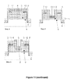
- FIG. 11 An exemplary process which is illustrated in Figure 11 may, for example, comprise:
- Fig. 15 shows in a cross-sectional drawing a further embodiment according to the invention.
- a third active layer 21 is present between the first active layer 3 and the substrate 1. While in the previous embodiments the first active layer 3 was shown as the top layer of the buffer layer 2, it is here a separate layer of GaN.
- the third active layer 21 is preferably an AlGaN buffer layer.
- the buffer layer 2 is for instance a GaN layer, but may alternatively a layer stack of AIN and AlGaN.
- the function of the buffer layer 2 is to match the lattice of the silicon substrate 1 with that of the AlGaN and GaN layers. Therewith it reduces strain.
- a plurality of layers in the stack is epitaxially grown in one reactor without intermediate removal of the substrate out of the reactor. This leads to a better matching of the layers and therefore also a better layer quality.
- the complete layer stack from the buffer layer 2 up to the passivation layer 11 is grown in a single sequence without intermediate removal of the substrate from the reactor.
- the thickness of the first active layer 3 is between 10 nm and 500 nm, preferably 100 to 200 nm, for instance 150 nm.
- the thickness of the third active layer 21 is higher than 500 nm, preferably higher than 1000 nm or even higher. In this particular example, the thickness of the third active layer 21 is 2 ⁇ m. Its Al content is between 5% and 100%, preferably between 8% and 18%.
- the third active layer 21 is selected such that its polarisation is higher than the bandgap of the first active layer 3.
- the bandgap of the third active layer 21 is higher than the bandgap of the first active layer 3 as well.
- Figures 12 and 13 relate to the thermal stability enhancement of the gate characteristics using the InAlN oxide.
- the devices in this example were grown by MOCVD on (111) Si substrates. They consist of a GaN buffer layer and an AIN layer on top of the GaN buffer layer.
- This device is also called "SiN/AlGaN/GaN heterostructure”.
- the samples In vacuum the samples have been heated in intervals of 100°C and kept at the temperature for 30 min. At each temperature step the sample was cooled down to the room temperature and data were taken to evaluate permanent degradation.
- the sheet resistance, the mobility and the density of the 2-DEG were characterized using the Van der Pauw Hall measurement. I-V measurements were performed to characterize the Schottky contacts.
- Figure 13 represents the 2-DEG densities (Ns: square), mobility ( ⁇ : circle) and sheet resistances (R ⁇ : triangle) as a function of annealing temperature in (a) SiN/Al 0.3 Ga 0.7 N/GaN, (b) In 0.18 Al 0.82 N/GaN.
- the "SiN/AlGaN/GaN heterostructure" is found to be fully stable up to 900°C ( Fig. 13a ). In the case of unstrained In 0.18 Al 0.82 N/GaN, no degradation of the 2-DEG behavior is noticed.
- Fig. 12 shows the Schottky contact characteristics as a function of the annealing temperature of the SiN/AlGaN/GaN heterostructure and the Al 2 O 3 /InAlN/GaN heterostructures. 10 diodes have been characterized for each sample. Even though the material properties of SiN/AlGaN/GaN system are stable at 700°C, an increase of the leakage current is observed giving rise to an almost ohmic contact (see inset of Fig. 12.a ). This is attributed to the diffusion of the gate metal into the barrier layer. Similar degradation at 700°C has been obtained with SiN/AIN/GaN devices.
- the use of the InAlN native oxide (Al 2 O 3 ) enables not only an exponential reduction of the gate leakage current and thus a significant increase of the gate breakdown voltage as a function of the oxidation time but also an enhanced device thermal stability up to at least 900°C (see Fig. 12.b ). It has to be pointed out that for 10 min thermal oxidation the turn-on voltage is shifted from 1.5 V to more than 15 V as compared to the reference sample while marginal gate leakage degradation occurred after 30 min at 900°C, illustrating the highly insulating oxide film property.
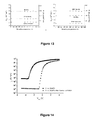
- Figure 14 shows the drain current I d as a function of the gate voltage V gs for a prior art device and a device according to the invention.
- the upper line corresponds to the prior art device and the lower line corresponds to the device according to the invention.
- This figure shows results from experiments carried out with a device structure as shown in Fig. 4 , having a AlGaN buffer layer 2, including the first active layer, on the substrate 1. Thereon, a spacer layer 13 (also channel) is present.
- the second active layer 4 is present, comprising a 1 nm undoped layer 14 and a 6 nm highly doped layer 15.
- the structure is covered with source and drain contacts 7, 8, a metal gate contact and a passivation layer.
- the gate insulating layer is generated by local thermal oxidation of the highly doped layer 15. In the prior art device, there was no thermal oxidation and the gate is in contact with the highly doped layer 15.
- the use of a thermal oxide as a gate insulating layer significantly improves the properties of the device.
- the oxidation step causes a significant shift of the threshold voltage up to 0 V. Additionally it lowers the drain current (i.e. it reduces the leakage current) of the device. It is clear from these results that the conversion of the InAlN into Al-oxide can locally deplete the 2-DEG. The same results were also obtained using a 8 nm thick InAlN barrier layer.
Landscapes
- Insulated Gate Type Field-Effect Transistor (AREA)
- Junction Field-Effect Transistors (AREA)
- Thin Film Transistor (AREA)
Priority Applications (1)
| Application Number | Priority Date | Filing Date | Title |
|---|---|---|---|
| EP09165584.5A EP2146378B1 (de) | 2008-07-15 | 2009-07-15 | Halbleitervorrichtung |
Applications Claiming Priority (3)
| Application Number | Priority Date | Filing Date | Title |
|---|---|---|---|
| US8098308P | 2008-07-15 | 2008-07-15 | |
| EP08169271 | 2008-11-17 | ||
| EP09165584.5A EP2146378B1 (de) | 2008-07-15 | 2009-07-15 | Halbleitervorrichtung |
Publications (3)
| Publication Number | Publication Date |
|---|---|
| EP2146378A2 true EP2146378A2 (de) | 2010-01-20 |
| EP2146378A3 EP2146378A3 (de) | 2010-04-28 |
| EP2146378B1 EP2146378B1 (de) | 2019-10-09 |
Family
ID=40361766
Family Applications (1)
| Application Number | Title | Priority Date | Filing Date |
|---|---|---|---|
| EP09165584.5A Active EP2146378B1 (de) | 2008-07-15 | 2009-07-15 | Halbleitervorrichtung |
Country Status (3)
| Country | Link |
|---|---|
| US (2) | US8309987B2 (de) |
| EP (1) | EP2146378B1 (de) |
| JP (1) | JP2010045343A (de) |
Cited By (3)
| Publication number | Priority date | Publication date | Assignee | Title |
|---|---|---|---|---|
| CN103681831A (zh) * | 2012-09-14 | 2014-03-26 | 中国科学院微电子研究所 | 高电子迁移率晶体管及其制造方法 |
| CN106328700A (zh) * | 2016-08-22 | 2017-01-11 | 东南大学 | 一种增强型绝缘埋层AlGaN‑GaN高电子迁移率晶体管 |
| CN107230707A (zh) * | 2016-03-25 | 2017-10-03 | 北京大学 | 半导体器件及制造方法 |
Families Citing this family (88)
| Publication number | Priority date | Publication date | Assignee | Title |
|---|---|---|---|---|
| US7417266B1 (en) | 2004-06-10 | 2008-08-26 | Qspeed Semiconductor Inc. | MOSFET having a JFET embedded as a body diode |
| JP5487615B2 (ja) * | 2008-12-24 | 2014-05-07 | サンケン電気株式会社 | 電界効果半導体装置及びその製造方法 |
| JP5531673B2 (ja) | 2009-04-06 | 2014-06-25 | 株式会社デンソー | ステータコイルのコイルエンド成形方法および成形装置 |
| JP5562579B2 (ja) * | 2009-05-12 | 2014-07-30 | 日本碍子株式会社 | 半導体素子用エピタキシャル基板の作製方法 |
| US8624260B2 (en) * | 2010-01-30 | 2014-01-07 | National Semiconductor Corporation | Enhancement-mode GaN MOSFET with low leakage current and improved reliability |
| US20110210377A1 (en) * | 2010-02-26 | 2011-09-01 | Infineon Technologies Austria Ag | Nitride semiconductor device |
| KR101679054B1 (ko) * | 2010-05-04 | 2016-11-25 | 삼성전자주식회사 | 산소처리영역을 포함하는 고 전자 이동도 트랜지스터 및 그 제조방법 |
| KR20110122525A (ko) * | 2010-05-04 | 2011-11-10 | 삼성전자주식회사 | Ldd 영역을 갖는 고 전자 이동도 트랜지스터(hemt) 및 그 제조방법 |
| US8878246B2 (en) | 2010-06-14 | 2014-11-04 | Samsung Electronics Co., Ltd. | High electron mobility transistors and methods of fabricating the same |
| JPWO2012014675A1 (ja) * | 2010-07-29 | 2013-09-12 | 日本碍子株式会社 | 半導体素子、hemt素子、および半導体素子の製造方法 |
| KR101652403B1 (ko) * | 2010-08-13 | 2016-08-31 | 삼성전자주식회사 | 전력 전자소자 및 그 제조방법 |
| CN103081080B (zh) | 2010-08-25 | 2016-01-13 | 日本碍子株式会社 | 半导体元件用外延基板、半导体元件、半导体元件用外延基板的制作方法、以及半导体元件的制作方法 |
| JP5913816B2 (ja) | 2011-02-21 | 2016-04-27 | 富士通株式会社 | 半導体装置の製造方法 |
| US8653559B2 (en) * | 2011-06-29 | 2014-02-18 | Hrl Laboratories, Llc | AlGaN/GaN hybrid MOS-HFET |
| US8633095B2 (en) * | 2011-06-30 | 2014-01-21 | Infineon Technologies Austria Ag | Semiconductor device with voltage compensation structure |
| KR20130004760A (ko) | 2011-07-04 | 2013-01-14 | 삼성전자주식회사 | 파워소자 및 이의 제조방법 |
| US20130026480A1 (en) * | 2011-07-25 | 2013-01-31 | Bridgelux, Inc. | Nucleation of Aluminum Nitride on a Silicon Substrate Using an Ammonia Preflow |
| JP5878317B2 (ja) * | 2011-08-08 | 2016-03-08 | ルネサスエレクトロニクス株式会社 | 半導体装置及び半導体装置の製造方法 |
| JP5827529B2 (ja) * | 2011-09-15 | 2015-12-02 | ローム株式会社 | 窒化物半導体装置およびその製造方法 |
| US8633094B2 (en) | 2011-12-01 | 2014-01-21 | Power Integrations, Inc. | GaN high voltage HFET with passivation plus gate dielectric multilayer structure |
| US20130143392A1 (en) * | 2011-12-06 | 2013-06-06 | Epowersoft, Inc. | In-situ sin growth to enable schottky contact for gan devices |
| US8940620B2 (en) | 2011-12-15 | 2015-01-27 | Power Integrations, Inc. | Composite wafer for fabrication of semiconductor devices |
| US8680535B2 (en) | 2011-12-23 | 2014-03-25 | Taiwan Semiconductor Manufacturing Company, Ltd. | High electron mobility transistor structure with improved breakdown voltage performance |
| US8669591B2 (en) * | 2011-12-27 | 2014-03-11 | Eta Semiconductor Inc. | E-mode HFET device |
| JP5750382B2 (ja) * | 2012-02-15 | 2015-07-22 | シャープ株式会社 | 窒化物半導体装置 |
| JP6054620B2 (ja) * | 2012-03-29 | 2016-12-27 | トランスフォーム・ジャパン株式会社 | 化合物半導体装置及びその製造方法 |
| US20130313561A1 (en) * | 2012-05-25 | 2013-11-28 | Triquint Semiconductor, Inc. | Group iii-nitride transistor with charge-inducing layer |
| US9443941B2 (en) * | 2012-06-04 | 2016-09-13 | Infineon Technologies Austria Ag | Compound semiconductor transistor with self aligned gate |
| CN102810564B (zh) * | 2012-06-12 | 2017-03-15 | 苏州能讯高能半导体有限公司 | 一种射频器件及其制作方法 |
| US8884268B2 (en) * | 2012-07-16 | 2014-11-11 | Taiwan Semiconductor Manufacturing Co., Ltd. | Diffusion barrier layer for group III nitride on silicon substrate |
| US20140077266A1 (en) * | 2012-09-14 | 2014-03-20 | Power Integrations, Inc. | Heterostructure Transistor with Multiple Gate Dielectric Layers |
| US9373689B2 (en) * | 2012-12-28 | 2016-06-21 | Taiwan Semiconductor Manufacturing Company, Ltd. | High electron mobility transistor and method of forming the same |
| JP6253886B2 (ja) * | 2013-01-09 | 2017-12-27 | トランスフォーム・ジャパン株式会社 | 半導体装置及び半導体装置の製造方法 |
| US10164038B2 (en) | 2013-01-30 | 2018-12-25 | Taiwan Semiconductor Manufacturing Company, Ltd. | Method of implanting dopants into a group III-nitride structure and device formed |
| US8928037B2 (en) | 2013-02-28 | 2015-01-06 | Power Integrations, Inc. | Heterostructure power transistor with AlSiN passivation layer |
| US9166005B2 (en) | 2013-03-01 | 2015-10-20 | Infineon Technologies Austria Ag | Semiconductor device with charge compensation structure |
| US9111956B2 (en) * | 2013-03-14 | 2015-08-18 | Taiwan Semiconductor Manufacturing Company, Ltd. | Rectifier structures with low leakage |
| US9455341B2 (en) * | 2013-07-17 | 2016-09-27 | Taiwan Semiconductor Manufacturing Company, Ltd. | Transistor having a back-barrier layer and method of making the same |
| US9076854B2 (en) * | 2013-08-26 | 2015-07-07 | Taiwan Semiconductor Manufacturing Company, Ltd. | Semiconductor device |
| JP2015073073A (ja) * | 2013-09-06 | 2015-04-16 | 三菱電機株式会社 | 半導体装置およびその製造方法 |
| JP6287143B2 (ja) | 2013-12-06 | 2018-03-07 | 株式会社デンソー | 半導体装置およびその製造方法 |
| KR102021887B1 (ko) | 2013-12-09 | 2019-09-17 | 삼성전자주식회사 | 반도체 소자 |
| US10407716B2 (en) * | 2014-03-13 | 2019-09-10 | Duke University | Electronic platform for sensing and control of electrochemical reactions |
| JP2016162889A (ja) * | 2015-03-02 | 2016-09-05 | 富士通株式会社 | 半導体装置及び半導体装置の製造方法 |
| US9412830B2 (en) | 2014-04-17 | 2016-08-09 | Fujitsu Limited | Semiconductor device and method of manufacturing semiconductor device |
| JP6237433B2 (ja) * | 2014-04-17 | 2017-11-29 | 富士通株式会社 | 半導体装置及び半導体装置の製造方法 |
| CN105304704A (zh) | 2014-05-30 | 2016-02-03 | 台达电子工业股份有限公司 | 半导体装置与其的制造方法 |
| JP2017533574A (ja) | 2014-09-18 | 2017-11-09 | インテル・コーポレーション | シリコンcmos互換性半導体装置における欠陥伝播制御のための傾斜側壁カット面を有するウルツ鉱ヘテロエピタキシャル構造物 |
| WO2016048328A1 (en) | 2014-09-25 | 2016-03-31 | Intel Corporation | Iii-n epitaxial device structures on free standing silicon mesas |
| US9640620B2 (en) * | 2014-11-03 | 2017-05-02 | Texas Instruments Incorporated | High power transistor with oxide gate barriers |
| US10573647B2 (en) | 2014-11-18 | 2020-02-25 | Intel Corporation | CMOS circuits using n-channel and p-channel gallium nitride transistors |
| CN104835819B (zh) * | 2014-12-04 | 2018-03-20 | 中国电子科技集团公司第五十五研究所 | 一种基于二次氧化法的GaN E/D集成器件制备方法 |
| CN106922200B (zh) | 2014-12-18 | 2021-11-09 | 英特尔公司 | N沟道氮化镓晶体管 |
| JP6401053B2 (ja) | 2014-12-26 | 2018-10-03 | ルネサスエレクトロニクス株式会社 | 半導体装置および半導体装置の製造方法 |
| JP6496149B2 (ja) * | 2015-01-22 | 2019-04-03 | ローム株式会社 | 半導体装置および半導体装置の製造方法 |
| US9653570B2 (en) * | 2015-02-12 | 2017-05-16 | International Business Machines Corporation | Junction interlayer dielectric for reducing leakage current in semiconductor devices |
| US10211327B2 (en) | 2015-05-19 | 2019-02-19 | Intel Corporation | Semiconductor devices with raised doped crystalline structures |
| EP3314659A4 (de) * | 2015-06-26 | 2019-01-23 | INTEL Corporation | Heteroepitaxiestrukturen mit hochtemperaturbeständigem substratzwischenmaterial |
| CN105185827A (zh) * | 2015-09-08 | 2015-12-23 | 东南大学 | 一种AlGaN/GaN高电子迁移率功率半导体器件 |
| US10381455B1 (en) | 2015-09-11 | 2019-08-13 | United States Of America As Represented By The Administrator Of National Aeronautics And Space Administration | Diffusion barrier systems (DBS) for high temperature semiconductor electrical contacts |
| JP6584253B2 (ja) * | 2015-09-16 | 2019-10-02 | ローム株式会社 | SiCエピタキシャルウェハ、SiCエピタキシャルウェハの製造装置、SiCエピタキシャルウェハの製造方法、および半導体装置 |
| JP6631160B2 (ja) | 2015-10-29 | 2020-01-15 | 富士通株式会社 | 半導体装置、電源装置、高周波増幅器 |
| ITUB20155503A1 (it) | 2015-11-12 | 2017-05-12 | St Microelectronics Srl | Metodo di fabbricazione di un transistore hemt e transistore hemt con migliorata mobilita' elettronica |
| WO2017111869A1 (en) | 2015-12-24 | 2017-06-29 | Intel Corporation | Transition metal dichalcogenides (tmdcs) over iii-nitride heteroepitaxial layers |
| JP6852283B2 (ja) * | 2016-05-25 | 2021-03-31 | 富士通株式会社 | 半導体装置の製造方法 |
| CN106449406B (zh) * | 2016-05-30 | 2020-05-12 | 湖南理工学院 | 一种垂直结构GaN基增强型场效应晶体管及其制造方法 |
| JP2018056319A (ja) | 2016-09-28 | 2018-04-05 | 富士通株式会社 | 半導体装置、半導体装置の製造方法、電源装置及び増幅器 |
| KR101811808B1 (ko) * | 2016-12-19 | 2017-12-22 | 삼성전자주식회사 | Ldd 영역을 갖는 고 전자 이동도 트랜지스터(hemt) 및 그 제조방법 |
| US9960265B1 (en) * | 2017-02-02 | 2018-05-01 | Semiconductor Components Industries, Llc | III-V semiconductor device and method therefor |
| CN106981512B (zh) * | 2017-03-27 | 2019-12-13 | 西安交通大学 | 金刚石基常关型场效应晶体管及其制备方法 |
| US11235793B1 (en) | 2017-09-16 | 2022-02-01 | The Tuway American Group, Inc. | Check list stand for use in health care settings such as cleaning supply carts for hospital environments and cleaning carts for the same |
| US11233053B2 (en) | 2017-09-29 | 2022-01-25 | Intel Corporation | Group III-nitride (III-N) devices with reduced contact resistance and their methods of fabrication |
| WO2019066935A1 (en) | 2017-09-29 | 2019-04-04 | Intel Corporation | REDUCED CONTACT RESISTANCE GROUP III (N-N) NITRIDE DEVICES AND METHODS OF MAKING THE SAME |
| CN109659361B (zh) | 2017-10-12 | 2022-03-04 | 电力集成公司 | 用于异质结器件的栅极堆叠体 |
| US11489061B2 (en) * | 2018-09-24 | 2022-11-01 | Intel Corporation | Integrated programmable gate radio frequency (RF) switch |
| US10937873B2 (en) * | 2019-01-03 | 2021-03-02 | Cree, Inc. | High electron mobility transistors having improved drain current drift and/or leakage current performance |
| TWI851591B (zh) * | 2019-08-06 | 2024-08-11 | 英商Iqe有限公司 | 分層結構的介電鈍化 |
| CN118039685A (zh) * | 2019-10-09 | 2024-05-14 | 联华电子股份有限公司 | 高电子迁移率晶体管及其制作方法 |
| CN111640796A (zh) * | 2020-06-01 | 2020-09-08 | 西安电子科技大学 | 5G民用射频GaN基HEMT器件、MOS-HEMT器件及制备方法 |
| JP2021044588A (ja) * | 2020-12-17 | 2021-03-18 | 富士通株式会社 | 半導体装置及び半導体装置の製造方法 |
| CN112993029B (zh) * | 2021-02-04 | 2022-04-01 | 宁波海特创电控有限公司 | 一种提高GaN HEMT界面质量的方法 |
| TWI921550B (zh) * | 2021-06-11 | 2026-04-11 | 南韓商周星工程股份有限公司 | 用於製造功率半導體元件的方法 |
| CN113451394B (zh) * | 2021-06-30 | 2023-04-28 | 深圳市时代速信科技有限公司 | 半导体器件和半导体器件制作方法 |
| US12218202B2 (en) * | 2021-09-16 | 2025-02-04 | Wolfspeed, Inc. | Semiconductor device incorporating a substrate recess |
| WO2023181749A1 (ja) * | 2022-03-25 | 2023-09-28 | ヌヴォトンテクノロジージャパン株式会社 | 半導体装置 |
| CN117352542A (zh) * | 2022-06-29 | 2024-01-05 | 华为技术有限公司 | 一种器件、模组和设备 |
| CN118202470A (zh) * | 2022-08-05 | 2024-06-14 | 英诺赛科(苏州)半导体有限公司 | 氮化物基半导体器件及其制造方法 |
| CN115799276B (zh) * | 2022-12-26 | 2026-07-03 | 武汉华星光电半导体显示技术有限公司 | 驱动基板及显示面板 |
Citations (3)
| Publication number | Priority date | Publication date | Assignee | Title |
|---|---|---|---|---|
| US5929467A (en) | 1996-12-04 | 1999-07-27 | Sony Corporation | Field effect transistor with nitride compound |
| US20070123003A1 (en) | 2005-11-30 | 2007-05-31 | Brask Justin K | Dielectric interface for group III-V semiconductor device |
| EP1865561A1 (de) | 2006-06-07 | 2007-12-12 | Interuniversitair Microelektronica Centrum (IMEC) | Feldeffektvorrichtung mit Verstärkungsmodus und Herstellungsverfahren dafür |
Family Cites Families (12)
| Publication number | Priority date | Publication date | Assignee | Title |
|---|---|---|---|---|
| WO2003015174A2 (en) * | 2001-08-07 | 2003-02-20 | Jan Kuzmik | High electron mobility devices |
| US6989556B2 (en) | 2002-06-06 | 2006-01-24 | Osemi, Inc. | Metal oxide compound semiconductor integrated transistor devices with a gate insulator structure |
| JP2004311869A (ja) * | 2003-04-10 | 2004-11-04 | Mitsubishi Electric Corp | 窒化物半導体系電界効果トランジスタとその製造方法 |
| JP2006032552A (ja) * | 2004-07-14 | 2006-02-02 | Toshiba Corp | 窒化物含有半導体装置 |
| EP1932181A4 (de) * | 2005-09-16 | 2009-06-17 | Univ California | N-polarer feldeffekttransistor mit aluminium-galliumnitrid-/galliumnitrid-verstärkungs-modus |
| US7399692B2 (en) | 2005-10-03 | 2008-07-15 | International Rectifier Corporation | III-nitride semiconductor fabrication |
| JP5041701B2 (ja) * | 2005-12-07 | 2012-10-03 | 日本電信電話株式会社 | ヘテロ接合型電界効果トランジスタ |
| JP5163129B2 (ja) | 2006-02-10 | 2013-03-13 | 日本電気株式会社 | 半導体装置 |
| JP5183975B2 (ja) * | 2006-06-07 | 2013-04-17 | アイメック | エンハンスモード電界効果デバイスおよびその製造方法 |
| US8399911B2 (en) * | 2006-06-07 | 2013-03-19 | Imec | Enhancement mode field effect device and the method of production thereof |
| US8476125B2 (en) * | 2006-12-15 | 2013-07-02 | University Of South Carolina | Fabrication technique for high frequency, high power group III nitride electronic devices |
| WO2008086001A2 (en) * | 2007-01-10 | 2008-07-17 | International Rectifier Corporation | Active area shaping for iii-nitride device and process for its manufacture |
-
2009
- 2009-07-14 US US12/502,960 patent/US8309987B2/en active Active
- 2009-07-15 EP EP09165584.5A patent/EP2146378B1/de active Active
- 2009-07-15 JP JP2009166622A patent/JP2010045343A/ja active Pending
-
2012
- 2012-10-12 US US13/651,192 patent/US8809138B2/en active Active
Patent Citations (3)
| Publication number | Priority date | Publication date | Assignee | Title |
|---|---|---|---|---|
| US5929467A (en) | 1996-12-04 | 1999-07-27 | Sony Corporation | Field effect transistor with nitride compound |
| US20070123003A1 (en) | 2005-11-30 | 2007-05-31 | Brask Justin K | Dielectric interface for group III-V semiconductor device |
| EP1865561A1 (de) | 2006-06-07 | 2007-12-12 | Interuniversitair Microelektronica Centrum (IMEC) | Feldeffektvorrichtung mit Verstärkungsmodus und Herstellungsverfahren dafür |
Non-Patent Citations (2)
| Title |
|---|
| LEE ET AL., IEEE TRANSACTIONS ON ELECTRON DEVICES, vol. 54, pages 41 - 424 |
| SUN ET AL., IEEE ELECTRON DEVICE LETTERS, vol. 28, 2007, pages 473 - 475 |
Cited By (4)
| Publication number | Priority date | Publication date | Assignee | Title |
|---|---|---|---|---|
| CN103681831A (zh) * | 2012-09-14 | 2014-03-26 | 中国科学院微电子研究所 | 高电子迁移率晶体管及其制造方法 |
| CN107230707A (zh) * | 2016-03-25 | 2017-10-03 | 北京大学 | 半导体器件及制造方法 |
| CN106328700A (zh) * | 2016-08-22 | 2017-01-11 | 东南大学 | 一种增强型绝缘埋层AlGaN‑GaN高电子迁移率晶体管 |
| CN106328700B (zh) * | 2016-08-22 | 2019-03-12 | 东南大学 | 一种增强型绝缘埋层AlGaN-GaN高电子迁移率晶体管 |
Also Published As
| Publication number | Publication date |
|---|---|
| US20100012977A1 (en) | 2010-01-21 |
| US8309987B2 (en) | 2012-11-13 |
| US20130102140A1 (en) | 2013-04-25 |
| JP2010045343A (ja) | 2010-02-25 |
| US8809138B2 (en) | 2014-08-19 |
| EP2146378B1 (de) | 2019-10-09 |
| EP2146378A3 (de) | 2010-04-28 |
Similar Documents
| Publication | Publication Date | Title |
|---|---|---|
| EP2146378B1 (de) | Halbleitervorrichtung | |
| US11705512B2 (en) | High electron mobility transistor (HEMT) and forming method thereof | |
| US9252258B2 (en) | CMOS compatible method for manufacturing a HEMT device and the HEMT device thereof | |
| US9130026B2 (en) | Crystalline layer for passivation of III-N surface | |
| US8900939B2 (en) | Transistor with enhanced channel charge inducing material layer and threshold voltage control | |
| US10367087B2 (en) | Transistor structure including a scandium gallium nitride back-barrier layer | |
| US8399911B2 (en) | Enhancement mode field effect device and the method of production thereof | |
| US9437685B2 (en) | Group III-V device with a selectively reduced impurity concentration | |
| JP5334149B2 (ja) | 窒化物半導体電界効果トランジスタ | |
| US20140335666A1 (en) | Growth of High-Performance III-Nitride Transistor Passivation Layer for GaN Electronics | |
| TWI765880B (zh) | 半導體結構、hemt結構及其形成方法 | |
| CN109819678A (zh) | 掺杂的栅极电介质材料 | |
| CN102694013A (zh) | 采用耗尽模式GaN基FET的串叠电路 | |
| CN101971307A (zh) | 半导体装置及半导体装置的制造方法 | |
| US20150060947A1 (en) | Transistor with Diamond Gate | |
| US12040380B2 (en) | High electron mobility transistor and method for fabricating the same | |
| EP1865561B1 (de) | Feldeffektvorrichtung mit Verstärkungsmodus und Herstellungsverfahren dafür | |
| KR101935928B1 (ko) | 게이트 누설 전류가 감소된 고 전자 이동도 트랜지스터 | |
| CN113826212A (zh) | 一种半导体结构的制备方法 | |
| EP1883115A1 (de) | Feldefftektbauelement vom Anreicherungs-Typ und Verfahren zu seiner Herstellung | |
| Chen et al. | Indium-based ternary barrier high-electron-mobility transistors on Si substrate with high ON/OFF ratio for power applications |
Legal Events
| Date | Code | Title | Description |
|---|---|---|---|
| PUAI | Public reference made under article 153(3) epc to a published international application that has entered the european phase |
Free format text: ORIGINAL CODE: 0009012 |
|
| AK | Designated contracting states |
Kind code of ref document: A2 Designated state(s): AT BE BG CH CY CZ DE DK EE ES FI FR GB GR HR HU IE IS IT LI LT LU LV MC MK MT NL NO PL PT RO SE SI SK SM TR |
|
| AX | Request for extension of the european patent |
Extension state: AL BA RS |
|
| PUAL | Search report despatched |
Free format text: ORIGINAL CODE: 0009013 |
|
| AK | Designated contracting states |
Kind code of ref document: A3 Designated state(s): AT BE BG CH CY CZ DE DK EE ES FI FR GB GR HR HU IE IS IT LI LT LU LV MC MK MT NL NO PL PT RO SE SI SK SM TR |
|
| AX | Request for extension of the european patent |
Extension state: AL BA RS |
|
| RAP1 | Party data changed (applicant data changed or rights of an application transferred) |
Owner name: IMEC |
|
| 17P | Request for examination filed |
Effective date: 20101028 |
|
| 17Q | First examination report despatched |
Effective date: 20101126 |
|
| RAP1 | Party data changed (applicant data changed or rights of an application transferred) |
Owner name: IMEC VZW |
|
| GRAP | Despatch of communication of intention to grant a patent |
Free format text: ORIGINAL CODE: EPIDOSNIGR1 |
|
| STAA | Information on the status of an ep patent application or granted ep patent |
Free format text: STATUS: GRANT OF PATENT IS INTENDED |
|
| RIC1 | Information provided on ipc code assigned before grant |
Ipc: H01L 29/423 20060101ALI20190604BHEP Ipc: H01L 23/29 20060101ALN20190604BHEP Ipc: H01L 29/417 20060101ALN20190604BHEP Ipc: H01L 29/51 20060101ALI20190604BHEP Ipc: H01L 29/778 20060101AFI20190604BHEP Ipc: H01L 23/31 20060101ALN20190604BHEP Ipc: H01L 21/336 20060101ALI20190604BHEP Ipc: H01L 29/20 20060101ALN20190604BHEP Ipc: H01L 29/06 20060101ALN20190604BHEP |
|
| INTG | Intention to grant announced |
Effective date: 20190628 |
|
| GRAS | Grant fee paid |
Free format text: ORIGINAL CODE: EPIDOSNIGR3 |
|
| GRAA | (expected) grant |
Free format text: ORIGINAL CODE: 0009210 |
|
| STAA | Information on the status of an ep patent application or granted ep patent |
Free format text: STATUS: THE PATENT HAS BEEN GRANTED |
|
| AK | Designated contracting states |
Kind code of ref document: B1 Designated state(s): AT BE BG CH CY CZ DE DK EE ES FI FR GB GR HR HU IE IS IT LI LT LU LV MC MK MT NL NO PL PT RO SE SI SK SM TR |
|
| REG | Reference to a national code |
Ref country code: GB Ref legal event code: FG4D |
|
| REG | Reference to a national code |
Ref country code: CH Ref legal event code: EP |
|
| REG | Reference to a national code |
Ref country code: IE Ref legal event code: FG4D |
|
| REG | Reference to a national code |
Ref country code: DE Ref legal event code: R096 Ref document number: 602009060059 Country of ref document: DE |
|
| REG | Reference to a national code |
Ref country code: AT Ref legal event code: REF Ref document number: 1189816 Country of ref document: AT Kind code of ref document: T Effective date: 20191115 |
|
| REG | Reference to a national code |
Ref country code: NL Ref legal event code: MP Effective date: 20191009 |
|
| REG | Reference to a national code |
Ref country code: LT Ref legal event code: MG4D |
|
| REG | Reference to a national code |
Ref country code: AT Ref legal event code: MK05 Ref document number: 1189816 Country of ref document: AT Kind code of ref document: T Effective date: 20191009 |
|
| PG25 | Lapsed in a contracting state [announced via postgrant information from national office to epo] |
Ref country code: NO Free format text: LAPSE BECAUSE OF FAILURE TO SUBMIT A TRANSLATION OF THE DESCRIPTION OR TO PAY THE FEE WITHIN THE PRESCRIBED TIME-LIMIT Effective date: 20200109 Ref country code: PL Free format text: LAPSE BECAUSE OF FAILURE TO SUBMIT A TRANSLATION OF THE DESCRIPTION OR TO PAY THE FEE WITHIN THE PRESCRIBED TIME-LIMIT Effective date: 20191009 Ref country code: PT Free format text: LAPSE BECAUSE OF FAILURE TO SUBMIT A TRANSLATION OF THE DESCRIPTION OR TO PAY THE FEE WITHIN THE PRESCRIBED TIME-LIMIT Effective date: 20200210 Ref country code: ES Free format text: LAPSE BECAUSE OF FAILURE TO SUBMIT A TRANSLATION OF THE DESCRIPTION OR TO PAY THE FEE WITHIN THE PRESCRIBED TIME-LIMIT Effective date: 20191009 Ref country code: NL Free format text: LAPSE BECAUSE OF FAILURE TO SUBMIT A TRANSLATION OF THE DESCRIPTION OR TO PAY THE FEE WITHIN THE PRESCRIBED TIME-LIMIT Effective date: 20191009 Ref country code: LT Free format text: LAPSE BECAUSE OF FAILURE TO SUBMIT A TRANSLATION OF THE DESCRIPTION OR TO PAY THE FEE WITHIN THE PRESCRIBED TIME-LIMIT Effective date: 20191009 Ref country code: LV Free format text: LAPSE BECAUSE OF FAILURE TO SUBMIT A TRANSLATION OF THE DESCRIPTION OR TO PAY THE FEE WITHIN THE PRESCRIBED TIME-LIMIT Effective date: 20191009 Ref country code: SE Free format text: LAPSE BECAUSE OF FAILURE TO SUBMIT A TRANSLATION OF THE DESCRIPTION OR TO PAY THE FEE WITHIN THE PRESCRIBED TIME-LIMIT Effective date: 20191009 Ref country code: AT Free format text: LAPSE BECAUSE OF FAILURE TO SUBMIT A TRANSLATION OF THE DESCRIPTION OR TO PAY THE FEE WITHIN THE PRESCRIBED TIME-LIMIT Effective date: 20191009 Ref country code: GR Free format text: LAPSE BECAUSE OF FAILURE TO SUBMIT A TRANSLATION OF THE DESCRIPTION OR TO PAY THE FEE WITHIN THE PRESCRIBED TIME-LIMIT Effective date: 20200110 Ref country code: FI Free format text: LAPSE BECAUSE OF FAILURE TO SUBMIT A TRANSLATION OF THE DESCRIPTION OR TO PAY THE FEE WITHIN THE PRESCRIBED TIME-LIMIT Effective date: 20191009 Ref country code: BG Free format text: LAPSE BECAUSE OF FAILURE TO SUBMIT A TRANSLATION OF THE DESCRIPTION OR TO PAY THE FEE WITHIN THE PRESCRIBED TIME-LIMIT Effective date: 20200109 |
|
| PG25 | Lapsed in a contracting state [announced via postgrant information from national office to epo] |
Ref country code: IS Free format text: LAPSE BECAUSE OF FAILURE TO SUBMIT A TRANSLATION OF THE DESCRIPTION OR TO PAY THE FEE WITHIN THE PRESCRIBED TIME-LIMIT Effective date: 20200224 Ref country code: HR Free format text: LAPSE BECAUSE OF FAILURE TO SUBMIT A TRANSLATION OF THE DESCRIPTION OR TO PAY THE FEE WITHIN THE PRESCRIBED TIME-LIMIT Effective date: 20191009 |
|
| REG | Reference to a national code |
Ref country code: DE Ref legal event code: R097 Ref document number: 602009060059 Country of ref document: DE |
|
| PG2D | Information on lapse in contracting state deleted |
Ref country code: IS |
|
| PG25 | Lapsed in a contracting state [announced via postgrant information from national office to epo] |
Ref country code: DK Free format text: LAPSE BECAUSE OF FAILURE TO SUBMIT A TRANSLATION OF THE DESCRIPTION OR TO PAY THE FEE WITHIN THE PRESCRIBED TIME-LIMIT Effective date: 20191009 Ref country code: RO Free format text: LAPSE BECAUSE OF FAILURE TO SUBMIT A TRANSLATION OF THE DESCRIPTION OR TO PAY THE FEE WITHIN THE PRESCRIBED TIME-LIMIT Effective date: 20191009 Ref country code: CZ Free format text: LAPSE BECAUSE OF FAILURE TO SUBMIT A TRANSLATION OF THE DESCRIPTION OR TO PAY THE FEE WITHIN THE PRESCRIBED TIME-LIMIT Effective date: 20191009 Ref country code: EE Free format text: LAPSE BECAUSE OF FAILURE TO SUBMIT A TRANSLATION OF THE DESCRIPTION OR TO PAY THE FEE WITHIN THE PRESCRIBED TIME-LIMIT Effective date: 20191009 Ref country code: IS Free format text: LAPSE BECAUSE OF FAILURE TO SUBMIT A TRANSLATION OF THE DESCRIPTION OR TO PAY THE FEE WITHIN THE PRESCRIBED TIME-LIMIT Effective date: 20200209 |
|
| PLBE | No opposition filed within time limit |
Free format text: ORIGINAL CODE: 0009261 |
|
| STAA | Information on the status of an ep patent application or granted ep patent |
Free format text: STATUS: NO OPPOSITION FILED WITHIN TIME LIMIT |
|
| PG25 | Lapsed in a contracting state [announced via postgrant information from national office to epo] |
Ref country code: SK Free format text: LAPSE BECAUSE OF FAILURE TO SUBMIT A TRANSLATION OF THE DESCRIPTION OR TO PAY THE FEE WITHIN THE PRESCRIBED TIME-LIMIT Effective date: 20191009 Ref country code: SM Free format text: LAPSE BECAUSE OF FAILURE TO SUBMIT A TRANSLATION OF THE DESCRIPTION OR TO PAY THE FEE WITHIN THE PRESCRIBED TIME-LIMIT Effective date: 20191009 Ref country code: IT Free format text: LAPSE BECAUSE OF FAILURE TO SUBMIT A TRANSLATION OF THE DESCRIPTION OR TO PAY THE FEE WITHIN THE PRESCRIBED TIME-LIMIT Effective date: 20191009 |
|
| 26N | No opposition filed |
Effective date: 20200710 |
|
| PG25 | Lapsed in a contracting state [announced via postgrant information from national office to epo] |
Ref country code: SI Free format text: LAPSE BECAUSE OF FAILURE TO SUBMIT A TRANSLATION OF THE DESCRIPTION OR TO PAY THE FEE WITHIN THE PRESCRIBED TIME-LIMIT Effective date: 20191009 |
|
| PG25 | Lapsed in a contracting state [announced via postgrant information from national office to epo] |
Ref country code: MC Free format text: LAPSE BECAUSE OF FAILURE TO SUBMIT A TRANSLATION OF THE DESCRIPTION OR TO PAY THE FEE WITHIN THE PRESCRIBED TIME-LIMIT Effective date: 20191009 |
|
| REG | Reference to a national code |
Ref country code: CH Ref legal event code: PL |
|
| GBPC | Gb: european patent ceased through non-payment of renewal fee |
Effective date: 20200715 |
|
| REG | Reference to a national code |
Ref country code: BE Ref legal event code: MM Effective date: 20200731 |
|
| PG25 | Lapsed in a contracting state [announced via postgrant information from national office to epo] |
Ref country code: GB Free format text: LAPSE BECAUSE OF NON-PAYMENT OF DUE FEES Effective date: 20200715 Ref country code: LU Free format text: LAPSE BECAUSE OF NON-PAYMENT OF DUE FEES Effective date: 20200715 Ref country code: LI Free format text: LAPSE BECAUSE OF NON-PAYMENT OF DUE FEES Effective date: 20200731 Ref country code: CH Free format text: LAPSE BECAUSE OF NON-PAYMENT OF DUE FEES Effective date: 20200731 |
|
| PG25 | Lapsed in a contracting state [announced via postgrant information from national office to epo] |
Ref country code: BE Free format text: LAPSE BECAUSE OF NON-PAYMENT OF DUE FEES Effective date: 20200731 |
|
| PG25 | Lapsed in a contracting state [announced via postgrant information from national office to epo] |
Ref country code: IE Free format text: LAPSE BECAUSE OF NON-PAYMENT OF DUE FEES Effective date: 20200715 |
|
| PG25 | Lapsed in a contracting state [announced via postgrant information from national office to epo] |
Ref country code: TR Free format text: LAPSE BECAUSE OF FAILURE TO SUBMIT A TRANSLATION OF THE DESCRIPTION OR TO PAY THE FEE WITHIN THE PRESCRIBED TIME-LIMIT Effective date: 20191009 Ref country code: MT Free format text: LAPSE BECAUSE OF FAILURE TO SUBMIT A TRANSLATION OF THE DESCRIPTION OR TO PAY THE FEE WITHIN THE PRESCRIBED TIME-LIMIT Effective date: 20191009 Ref country code: CY Free format text: LAPSE BECAUSE OF FAILURE TO SUBMIT A TRANSLATION OF THE DESCRIPTION OR TO PAY THE FEE WITHIN THE PRESCRIBED TIME-LIMIT Effective date: 20191009 |
|
| PG25 | Lapsed in a contracting state [announced via postgrant information from national office to epo] |
Ref country code: MK Free format text: LAPSE BECAUSE OF FAILURE TO SUBMIT A TRANSLATION OF THE DESCRIPTION OR TO PAY THE FEE WITHIN THE PRESCRIBED TIME-LIMIT Effective date: 20191009 |
|
| P01 | Opt-out of the competence of the unified patent court (upc) registered |
Effective date: 20230513 |
|
| REG | Reference to a national code |
Ref country code: DE Ref legal event code: R079 Ref document number: 602009060059 Country of ref document: DE Free format text: PREVIOUS MAIN CLASS: H01L0029778000 Ipc: H10D0030470000 |
|
| PGFP | Annual fee paid to national office [announced via postgrant information from national office to epo] |
Ref country code: DE Payment date: 20250620 Year of fee payment: 17 |
|
| PGFP | Annual fee paid to national office [announced via postgrant information from national office to epo] |
Ref country code: FR Payment date: 20260619 Year of fee payment: 18 |