EP2148355A1 - Procédé et dispositif de fabrication de panneau d'étanchéité et dispositif de fabrication d'un panneau d'affichage plasma - Google Patents
Procédé et dispositif de fabrication de panneau d'étanchéité et dispositif de fabrication d'un panneau d'affichage plasma Download PDFInfo
- Publication number
- EP2148355A1 EP2148355A1 EP08777030A EP08777030A EP2148355A1 EP 2148355 A1 EP2148355 A1 EP 2148355A1 EP 08777030 A EP08777030 A EP 08777030A EP 08777030 A EP08777030 A EP 08777030A EP 2148355 A1 EP2148355 A1 EP 2148355A1
- Authority
- EP
- European Patent Office
- Prior art keywords
- substrate
- sealing material
- sealing
- chamber
- manufacturing
- Prior art date
- Legal status (The legal status is an assumption and is not a legal conclusion. Google has not performed a legal analysis and makes no representation as to the accuracy of the status listed.)
- Granted
Links
- 238000004519 manufacturing process Methods 0.000 title claims abstract description 89
- 238000007789 sealing Methods 0.000 title claims abstract description 86
- 238000000034 method Methods 0.000 title claims abstract description 36
- 239000000758 substrate Substances 0.000 claims abstract description 253
- 239000003566 sealing material Substances 0.000 claims abstract description 150
- 238000000576 coating method Methods 0.000 claims abstract description 76
- 239000011248 coating agent Substances 0.000 claims abstract description 75
- 239000011230 binding agent Substances 0.000 claims abstract description 44
- 238000002844 melting Methods 0.000 claims abstract description 38
- 230000008018 melting Effects 0.000 claims abstract description 38
- 238000010030 laminating Methods 0.000 claims abstract description 10
- 230000015572 biosynthetic process Effects 0.000 claims description 35
- 239000011521 glass Substances 0.000 claims description 27
- 238000004320 controlled atmosphere Methods 0.000 claims description 16
- 230000001681 protective effect Effects 0.000 claims description 13
- 239000000945 filler Substances 0.000 claims description 9
- 239000000155 melt Substances 0.000 claims description 6
- 239000007789 gas Substances 0.000 description 41
- 238000001035 drying Methods 0.000 description 21
- 230000032683 aging Effects 0.000 description 18
- 230000006872 improvement Effects 0.000 description 17
- 238000000746 purification Methods 0.000 description 14
- 239000011347 resin Substances 0.000 description 13
- 229920005989 resin Polymers 0.000 description 13
- 238000005516 engineering process Methods 0.000 description 11
- 230000003750 conditioning effect Effects 0.000 description 10
- 239000000463 material Substances 0.000 description 10
- 230000002431 foraging effect Effects 0.000 description 9
- 238000010438 heat treatment Methods 0.000 description 9
- 239000012535 impurity Substances 0.000 description 8
- 238000012545 processing Methods 0.000 description 8
- 239000012298 atmosphere Substances 0.000 description 7
- 238000005192 partition Methods 0.000 description 7
- 238000010586 diagram Methods 0.000 description 6
- 238000011068 loading method Methods 0.000 description 6
- 239000002904 solvent Substances 0.000 description 6
- CURLTUGMZLYLDI-UHFFFAOYSA-N Carbon dioxide Chemical compound O=C=O CURLTUGMZLYLDI-UHFFFAOYSA-N 0.000 description 4
- 238000002474 experimental method Methods 0.000 description 4
- 238000005259 measurement Methods 0.000 description 4
- 230000007246 mechanism Effects 0.000 description 4
- UGFAIRIUMAVXCW-UHFFFAOYSA-N Carbon monoxide Chemical compound [O+]#[C-] UGFAIRIUMAVXCW-UHFFFAOYSA-N 0.000 description 3
- 229910002092 carbon dioxide Inorganic materials 0.000 description 3
- 239000001569 carbon dioxide Substances 0.000 description 3
- 229910002091 carbon monoxide Inorganic materials 0.000 description 3
- 239000003795 chemical substances by application Substances 0.000 description 3
- 230000006835 compression Effects 0.000 description 3
- 238000007906 compression Methods 0.000 description 3
- 230000006837 decompression Effects 0.000 description 3
- 230000002093 peripheral effect Effects 0.000 description 3
- 239000000843 powder Substances 0.000 description 3
- 230000008569 process Effects 0.000 description 3
- PNEYBMLMFCGWSK-UHFFFAOYSA-N aluminium oxide Inorganic materials [O-2].[O-2].[O-2].[Al+3].[Al+3] PNEYBMLMFCGWSK-UHFFFAOYSA-N 0.000 description 2
- 238000007796 conventional method Methods 0.000 description 2
- 238000003795 desorption Methods 0.000 description 2
- 238000007599 discharging Methods 0.000 description 2
- 230000000694 effects Effects 0.000 description 2
- 238000005566 electron beam evaporation Methods 0.000 description 2
- 238000012986 modification Methods 0.000 description 2
- 230000004048 modification Effects 0.000 description 2
- 238000005488 sandblasting Methods 0.000 description 2
- 238000004544 sputter deposition Methods 0.000 description 2
- XOLBLPGZBRYERU-UHFFFAOYSA-N tin dioxide Chemical compound O=[Sn]=O XOLBLPGZBRYERU-UHFFFAOYSA-N 0.000 description 2
- WUOACPNHFRMFPN-SECBINFHSA-N (S)-(-)-alpha-terpineol Chemical compound CC1=CC[C@@H](C(C)(C)O)CC1 WUOACPNHFRMFPN-SECBINFHSA-N 0.000 description 1
- 239000004925 Acrylic resin Substances 0.000 description 1
- 229920000178 Acrylic resin Polymers 0.000 description 1
- 239000001856 Ethyl cellulose Substances 0.000 description 1
- ZZSNKZQZMQGXPY-UHFFFAOYSA-N Ethyl cellulose Chemical compound CCOCC1OC(OC)C(OCC)C(OCC)C1OC1C(O)C(O)C(OC)C(CO)O1 ZZSNKZQZMQGXPY-UHFFFAOYSA-N 0.000 description 1
- 239000000020 Nitrocellulose Substances 0.000 description 1
- OAICVXFJPJFONN-UHFFFAOYSA-N Phosphorus Chemical compound [P] OAICVXFJPJFONN-UHFFFAOYSA-N 0.000 description 1
- FJWGYAHXMCUOOM-QHOUIDNNSA-N [(2s,3r,4s,5r,6r)-2-[(2r,3r,4s,5r,6s)-4,5-dinitrooxy-2-(nitrooxymethyl)-6-[(2r,3r,4s,5r,6s)-4,5,6-trinitrooxy-2-(nitrooxymethyl)oxan-3-yl]oxyoxan-3-yl]oxy-3,5-dinitrooxy-6-(nitrooxymethyl)oxan-4-yl] nitrate Chemical compound O([C@@H]1O[C@@H]([C@H]([C@H](O[N+]([O-])=O)[C@H]1O[N+]([O-])=O)O[C@H]1[C@@H]([C@@H](O[N+]([O-])=O)[C@H](O[N+]([O-])=O)[C@@H](CO[N+]([O-])=O)O1)O[N+]([O-])=O)CO[N+](=O)[O-])[C@@H]1[C@@H](CO[N+]([O-])=O)O[C@@H](O[N+]([O-])=O)[C@H](O[N+]([O-])=O)[C@H]1O[N+]([O-])=O FJWGYAHXMCUOOM-QHOUIDNNSA-N 0.000 description 1
- HDVBADNLSOCABY-UHFFFAOYSA-N [P]=O.[Sn] Chemical compound [P]=O.[Sn] HDVBADNLSOCABY-UHFFFAOYSA-N 0.000 description 1
- 229910052784 alkaline earth metal Inorganic materials 0.000 description 1
- 150000001342 alkaline earth metals Chemical class 0.000 description 1
- OVKDFILSBMEKLT-UHFFFAOYSA-N alpha-Terpineol Natural products CC(=C)C1(O)CCC(C)=CC1 OVKDFILSBMEKLT-UHFFFAOYSA-N 0.000 description 1
- 229940088601 alpha-terpineol Drugs 0.000 description 1
- QVGXLLKOCUKJST-UHFFFAOYSA-N atomic oxygen Chemical compound [O] QVGXLLKOCUKJST-UHFFFAOYSA-N 0.000 description 1
- 239000011324 bead Substances 0.000 description 1
- 238000005422 blasting Methods 0.000 description 1
- 235000021170 buffet Nutrition 0.000 description 1
- 239000000919 ceramic Substances 0.000 description 1
- 238000006243 chemical reaction Methods 0.000 description 1
- 238000002485 combustion reaction Methods 0.000 description 1
- 239000004020 conductor Substances 0.000 description 1
- 238000011109 contamination Methods 0.000 description 1
- 238000001816 cooling Methods 0.000 description 1
- 238000004090 dissolution Methods 0.000 description 1
- 238000005265 energy consumption Methods 0.000 description 1
- 229920001249 ethyl cellulose Polymers 0.000 description 1
- 235000019325 ethyl cellulose Nutrition 0.000 description 1
- 150000002500 ions Chemical class 0.000 description 1
- 239000007769 metal material Substances 0.000 description 1
- 238000002156 mixing Methods 0.000 description 1
- 239000000203 mixture Substances 0.000 description 1
- 238000000465 moulding Methods 0.000 description 1
- 229920001220 nitrocellulos Polymers 0.000 description 1
- 229910052760 oxygen Inorganic materials 0.000 description 1
- 239000001301 oxygen Substances 0.000 description 1
- 238000000059 patterning Methods 0.000 description 1
- 238000005498 polishing Methods 0.000 description 1
- 238000007639 printing Methods 0.000 description 1
- 230000005855 radiation Effects 0.000 description 1
- 230000009467 reduction Effects 0.000 description 1
- 238000007650 screen-printing Methods 0.000 description 1
- 238000000926 separation method Methods 0.000 description 1
- 229910052709 silver Inorganic materials 0.000 description 1
- 239000007787 solid Substances 0.000 description 1
- 238000004611 spectroscopical analysis Methods 0.000 description 1
- 238000012360 testing method Methods 0.000 description 1
- XLYOFNOQVPJJNP-UHFFFAOYSA-N water Substances O XLYOFNOQVPJJNP-UHFFFAOYSA-N 0.000 description 1
Images


Classifications
-
- H—ELECTRICITY
- H01—ELECTRIC ELEMENTS
- H01J—ELECTRIC DISCHARGE TUBES OR DISCHARGE LAMPS
- H01J11/00—Gas-filled discharge tubes with alternating current induction of the discharge, e.g. alternating current plasma display panels [AC-PDP]; Gas-filled discharge tubes without any main electrode inside the vessel; Gas-filled discharge tubes with at least one main electrode outside the vessel
- H01J11/20—Constructional details
- H01J11/48—Sealing, e.g. seals specially adapted for leading-in conductors
-
- H—ELECTRICITY
- H01—ELECTRIC ELEMENTS
- H01J—ELECTRIC DISCHARGE TUBES OR DISCHARGE LAMPS
- H01J11/00—Gas-filled discharge tubes with alternating current induction of the discharge, e.g. alternating current plasma display panels [AC-PDP]; Gas-filled discharge tubes without any main electrode inside the vessel; Gas-filled discharge tubes with at least one main electrode outside the vessel
- H01J11/10—AC-PDPs with at least one main electrode being out of contact with the plasma
- H01J11/12—AC-PDPs with at least one main electrode being out of contact with the plasma with main electrodes provided on both sides of the discharge space
-
- H—ELECTRICITY
- H01—ELECTRIC ELEMENTS
- H01J—ELECTRIC DISCHARGE TUBES OR DISCHARGE LAMPS
- H01J11/00—Gas-filled discharge tubes with alternating current induction of the discharge, e.g. alternating current plasma display panels [AC-PDP]; Gas-filled discharge tubes without any main electrode inside the vessel; Gas-filled discharge tubes with at least one main electrode outside the vessel
- H01J11/20—Constructional details
- H01J11/34—Vessels, containers or parts thereof, e.g. substrates
- H01J11/40—Layers for protecting or enhancing the electron emission, e.g. MgO layers
-
- H—ELECTRICITY
- H01—ELECTRIC ELEMENTS
- H01J—ELECTRIC DISCHARGE TUBES OR DISCHARGE LAMPS
- H01J9/00—Apparatus or processes specially adapted for the manufacture, installation, removal, maintenance of electric discharge tubes, discharge lamps, or parts thereof; Recovery of material from discharge tubes or lamps
- H01J9/24—Manufacture or joining of vessels, leading-in conductors or bases
- H01J9/26—Sealing together parts of vessels
- H01J9/261—Sealing together parts of vessels the vessel being for a flat panel display
-
- H—ELECTRICITY
- H01—ELECTRIC ELEMENTS
- H01J—ELECTRIC DISCHARGE TUBES OR DISCHARGE LAMPS
- H01J9/00—Apparatus or processes specially adapted for the manufacture, installation, removal, maintenance of electric discharge tubes, discharge lamps, or parts thereof; Recovery of material from discharge tubes or lamps
- H01J9/40—Closing vessels
-
- H—ELECTRICITY
- H01—ELECTRIC ELEMENTS
- H01J—ELECTRIC DISCHARGE TUBES OR DISCHARGE LAMPS
- H01J2209/00—Apparatus and processes for manufacture of discharge tubes
- H01J2209/38—Control of maintenance of pressure in the vessel
- H01J2209/389—Degassing
- H01J2209/3896—Degassing by heating
-
- H—ELECTRICITY
- H01—ELECTRIC ELEMENTS
- H01J—ELECTRIC DISCHARGE TUBES OR DISCHARGE LAMPS
- H01J2329/00—Electron emission display panels, e.g. field emission display panels
- H01J2329/86—Vessels
- H01J2329/867—Seals between parts of vessels
-
- Y—GENERAL TAGGING OF NEW TECHNOLOGICAL DEVELOPMENTS; GENERAL TAGGING OF CROSS-SECTIONAL TECHNOLOGIES SPANNING OVER SEVERAL SECTIONS OF THE IPC; TECHNICAL SUBJECTS COVERED BY FORMER USPC CROSS-REFERENCE ART COLLECTIONS [XRACs] AND DIGESTS
- Y10—TECHNICAL SUBJECTS COVERED BY FORMER USPC
- Y10T—TECHNICAL SUBJECTS COVERED BY FORMER US CLASSIFICATION
- Y10T156/00—Adhesive bonding and miscellaneous chemical manufacture
- Y10T156/10—Methods of surface bonding and/or assembly therefor
Definitions
- the present invention relates to method and apparatus for manufacturing a sealed panel, and method and apparatus for manufacturing a plasma display panel.
- Priority is claimed on Japanese Patent Application No. 2007-153291, filed June 8, 2007 , the contents of which are incorporated herein by reference.
- PDP plasma display panels
- a front substrate and a rear substrate via a sealing material, and an electrical discharge gas is sealed thereinside.
- Three-electrode surface discharge technology is commonly used for PDPs in which sustaining electrodes and scanning electrodes are formed on the front substrate, and address electrodes are formed on the rear substrate.
- the sealed electrical discharge gas converted into plasma and ultraviolet rays are discharged.
- Phosphors which are formed on the rear substrate are excited by the ultraviolet rays resulting in visible light being discharged.
- a process for manufacturing a PDP includes a coating step of applying the sealing material onto a peripheral edge portion of the rear substrate, and a sealing step of laminating and sealing the front substrate and the rear substrate.
- the sealing material coating step the sealing agent transformed into paste is applied onto the rear substrate. Therefore, a sealing material is employed in which is mixed a binder which is made of solvent and resin component.
- a drying step is performed (for example, at a temperature of 120°C for 10 to 20 minutes) in order to remove the solvent, and a temporary baking step (for example, see Non-patent document 1) is also performed in order to remove the resin component.
- a rear substrate which has completed the drying step is firstly heated in air or in an oxygen atmosphere from a temperature of 120°C to 320°C over a temperature increase time of 5°C to 10°C per minute.
- the rear substrate is heated from a temperature of 320°C to 380°C at a temperature increase rate of 4°C per minute.
- the rear substrate is then held at a temperature of 380°C for 10 minutes.
- the rear substrate is cooled to room temperature at a temperature decrease rate of 5°C to 50°C per minute. It is noted that the heating is performed at a gentle pace is in order to ensure the dissolution and combustion of the binder.
- Resin component which remains in the sealing material changes into an impurity gas when the two substrates are being sealed together and contaminates the panel interior. Contamination caused by the resin component is one factor making it necessary to purify (i.e., dry) the interior of the panel by heating and evacuating (i.e., vacuum baking) for several hours during the sealing step.
- the present invention was conceived in order to solve the above described problem, and it is an object thereof to provide method and apparatus for manufacturing a sealed panel, and also method and apparatus for manufacturing a sealed panel which make it possible to achieve an improvement in throughput and energy efficiency.
- a method for manufacturing a sealed panel having a first substrate and a second substrate includes: a melting step of melting a sealing material which does not contain a binder for making the sealing material into paste form; a coating step of applying the melted sealing material onto a surface of the second substrate; and a sealing step of laminating the first substrate and the second substrate via the sealing material applied onto the surface of the second substrate.
- a sealing material which does not contain a binder since a sealing material which does not contain a binder is used, it is possible to greatly reduce the quantity of gas released from the sealing material. As a result, it is possible to considerably reduce the amount of time required to purify (i.e., dry) the panel interior in the sealing step, or else to eliminate the purification (i.e., drying) altogether. Further, it is also possible to considerably reduce the amount of time required for aging (i.e., pre-conditioning) after the sealing step, or else to eliminate the aging step altogether. Moreover, a binder removal step such as that required in the conventional technology is not necessary. Accordingly, it is possible to achieve an improvement in throughput and energy efficiency in manufacturing plasma display panels.
- the sealing material contains a low melting point glass. In this case, it is possible to reduce the quantity of gas released from the sealing material. Moreover, the coating and sealing can be performed at a comparatively low temperature. Further, air-tightness and cohesion strength after the sealing can be secured.
- the sealing material contains a low melting point glass and a filler.
- the coefficient of thermal expansion of the sealing material becomes close to the coefficients of thermal expansion of the first substrate and second substrate, the air-tightness and cohesion strength after the sealing can be secured.
- the method further includes a step of emitting gas contained within the melted sealing material.
- the gas existing inside the applied sealing material has been expelled therefrom, it is possible to further reduce the quantity of gas released from the sealing material.
- a method for manufacturing a plasma display panel having a first substrate and a second substrate includes: a melting step of melting a sealing material which does not contain a binder for making the sealing material into paste form; a baking step of baking phosphors applied onto the second substrate; a coating step of applying the melted sealing material onto a surface of the second substrate; and a sealing step of laminating the first substrate and the second substrate via the sealing material applied onto the surface of the second substrate, wherein the temperature of the second substrate is held at 100°C or more from the baking step through the coating step.
- the melted sealing material can be applied onto the surface of the second substrate.
- the second substrate is held in a vacuum or a controlled atmosphere from the baking step through the sealing step.
- a sealing material which does not contain a binder since a sealing material which does not contain a binder is used, it is not necessary to perform the drying step and baking step in the atmosphere for removing the binder. Because of this, it is possible to introduce the second substrate to the sealing step after the phosphors have been baked while maintaining it in a vacuum or in a controlled atmosphere, and thus preventing any impurity gas from adsorbing to the second substrate. As a result, it is possible to considerably reduce the amount of time required to purify (i.e., dry) the panel interior in the sealing step, or else to eliminate this purification (i.e., drying) altogether.
- another method for manufacturing a plasma display panel having a first substrate and a second substrate includes: a film formation step of forming a protective film on the first substrate at a size corresponding to the first substrate; a melting step of melting a sealing material which does not contain a binder for making the sealing material into paste form; a baking step of baking phosphors applied onto the second substrate are baked; a coating step of applying the melted sealing material onto a surface of the second substrate; and a sealing step of laminating a plurality of pairs of the first substrate and the second substrate in parallel via the sealing material applied onto the surface of each of the second substrates, wherein the temperature of the second substrates is held at 100°C or more from the baking step through the coating step.
- first substrates and second substrates which correspond to the sizes of the respective plasma display panels are laminated to each other. In this case, it is possible to efficiently manufacture panels of different sizes.
- an apparatus for manufacturing a sealed panel having a first substrate and a second substrate includes: a coating chamber in which a sealing material which does not contain a binder for making the sealing material into paste form is applied onto a surface of the second substrate in a vacuum or in a controlled atmosphere; a coating device which is provided in the coating chamber and applies the sealing material filled inside the coating device onto the surface of the second substrate; a heater which is provided in the coating device and melts the filled sealing material; and a sealing chamber in which the first substrate and the second substrate are laminated to each other via the sealing material.
- An apparatus for manufacturing a plasma display panel having a first substrate and a second substrate includes: a baking chamber in which phosphors applied onto the second substrate are baked; a coating chamber in which a sealing material which does not contain a binder for making the sealing material into paste form is applied onto a surface of the baked second substrate in a vacuum or in a controlled atmosphere; a coating device which is provided in the coating chamber and applies the sealing material filled inside the coating device onto the surface of the second substrate; a heater which is provided in the coating device and melts the filled sealing material; and a sealing chamber in which the first substrate and the second substrate are laminated to each other via the sealing material, wherein the second substrate is transported from the baking chamber through the coating chamber while the temperature thereof is held at 100°C or more.
- the second substrate is transported from the baking chamber through the sealing chamber while being held in a vacuum or in a controlled atmosphere.
- a sealing material which does not contain a binder is used, it is not necessary to perform the drying step and baking step in the atmosphere for removing the binder in the atmosphere. Because of this, it is possible to introduce the second substrate to the sealing step after the phosphors have been baked while maintaining it in a vacuum or in a controlled atmosphere, and thus preventing any impurity gas from adsorbing to the second substrate. As a result, it is possible to considerably reduce the amount of time required to purify (i.e., dry) the panel interior in the sealing step, or else to eliminate this purification (i.e., drying) altogether.
- another apparatus for manufacturing a plasma display panel having a first substrate and a second substrate includes: a film formation chamber in which a protective film is formed on the first substrate; a baking chamber in which phosphors applied onto the second substrate are baked; a coating chamber in which a sealing material which does not contain a binder for making the sealing material into paste form is applied onto a surface of the baked second substrate in a vacuum or in a controlled atmosphere; a coating device which is provided in the coating chamber and applies the sealing material filled inside the coating device onto the surface of the second substrate; a heater which is provided in the coating device and melts the filled sealing material; and a plurality of sealing chambers which are connected to the film formation chamber and in which the first substrate and the second substrate are laminated to each other via the sealing material, wherein the second substrates are transported from the baking chamber through the coating chamber while the temperature thereof is held at 100°C or more.
- first substrates and second substrates which correspond to the sizes of the respective plasma display panels are laminated to each other. In this case, it is possible to efficiently manufacture panels of different sizes.
- the present invention by melting a sealing material which does not contain a binder, it is possible to apply the sealing material onto the surface of a second substrate. Moreover, since a sealing material which does not contain a binder is used, it is possible to greatly reduce the quantity of gas released from the sealing material. As a result, it is possible to considerably reduce the time required to purify (i.e., dry) the panel interior in the sealing step, or else to eliminate this purification (i.e., drying) altogether. Further, it is also possible to considerably reduce the amount of time required for aging (i.e., pre-conditioning) after the sealing step, or else to eliminate this aging step altogether. Moreover, a binder removal step such as that required in the conventional technology is not necessary. Accordingly, it is possible to achieve an improvement in throughput and energy efficiency in manufacturing plasma display panels.
- FIG. 1 is an exploded perspective view of a three-electrode AC type plasma display panel.
- the plasma display panel (hereinafter referred to as "PDP") 100 is provided with a rear substrate 2 and a front substrate 1 which are arranged so as to face each other and a plurality of electrical discharge chambers 16 which are formed between the substrates 1 and 2.
- Display electrodes 12 are formed in a stripe pattern at predetermined intervals on the inner face of the front substrate 1.
- the display electrodes 12 are formed by a transparent conductive material such as ITO and bus electrodes.
- a dielectric layer 13 is formed so as to cover the display electrodes 12, and a protective film 14 is formed so as to cover the dielectric layer 13.
- the protective film 14 protects the dielectric layer 13 from positive ions which are generated through the conversion of the discharge gas into plasma, and is formed by an oxide of an alkaline earth metal such as MgO and SrO.
- address electrodes 11 are formed in a stripe pattern at predetermined intervals on the inner face of the rear substrate 2.
- the address electrodes 11 are arranged so as to be perpendicular to the display electrodes 12. Intersection points between the address electrodes 11 and the display electrodes 12 form pixels of the PDP 100.
- a dielectric layer 19 is formed so as to cover the address electrodes 11.
- partition walls (i.e., ribs) 15 are formed in parallel with the address electrodes 11 on the top face of the dielectric layer 19 between mutually adjacent address electrodes 11.
- phosphors 17 are placed on the top face of the dielectric layer 19 between mutually adjacent partition walls 15 and on the side faces of the partition walls 15. The phosphors 17 emit any one of red, green, or blue fluorescence.
- FIG 2A is a plan view of a PDP.
- the above described front substrate 1 and rear substrate 2 are laminated together by means of a sealing material 20 which is placed on peripheral edge portions of the inner faces of the substrates.
- FIG 2B is a side cross-sectional view taken along a line A-A in FIG 2A .
- electrical discharge chambers 16 are formed between mutually adjacent partition walls 15. Electrical discharge gas such as a mixture of Ne and Xe gases is sealed inside the electrical discharge chambers 16.
- sealing material 20 it is necessary to employ a material which has a coefficient of thermal expansion close to that of glass substrates constituting the front substrate 1 and the rear substrate 2, which exhibits sufficient fluidity at the sealing temperature, and which does not soften at the gas emission/baking temperature. It is also necessary for the material to be able to maintain the air-tightness of the panel interior after sealing and ensure the strength of the panel cohesion but not to release impurity gas.
- a low melting point glass is desirable. Specific examples of such a low melting point glass is a PbO ⁇ B 2 O 3 -based non-crystalline glass (i.e., amorphous glass) having a melting point of approximately 400°C.
- a filler into the low melting point glass.
- a filler is a ceramic-based powder materials such as alumina or the like.
- glass which has an even lower melting point for example, tin-phosphorus oxide-based glass
- tin-phosphorus oxide-based glass may be employed in order to alleviate the effects due to the differences between the coefficient of thermal expansion of the sealing material 20 and the coefficient of thermal expansion of the glass substrate.
- crystalline glass having a coefficient of thermal expansion close to that of the glass substrate may also be employed even if the melting point is higher than a low melting point glass. Further, it is desirable to improve the wettability between the low melting point glass and the substrate in order to enhance the fluidity thereof at the sealing temperature.
- a binder is mixed into the sealing material in order to make the sealing material into paste form.
- the binder is formed from a solvent and a resin component.
- the solvent is used to make the sealing agent into paste form, and is formed by ⁇ -terpineol or the like.
- the resin component is used to disperse solids in the paste, and is formed by ethyl cellulose, cellulose nitrate, acrylic resin, or the like. It is necessary to completely remove the binder after the sealing material has been applied. This type of binder is not mixed into the sealing material 20 of the present embodiment.
- FIG. 3 is a flowchart showing the method for manufacturing a PDP according to a first embodiment of the present invention.
- the PDP manufacturing process is broadly divided into two steps, namely, a panel step (S50) and a module setting step (S52).
- the panel step (S50) is divided into a front substrate step (S60), a rear substrate step (S70), and a panel formation step (S80).
- the transparent electrodes used for the display electrodes 12 are formed (S62). Specifically, a transparent conductive film such as ITO or SnO 2 or the like is formed using a sputtering method or the like, and patterning is then performed so as to form the display electrodes 12. Next, in order to reduce the electrical resistance of the display electrodes 12 which are formed from the transparent conductive film, auxiliary electrodes (i.e., bus electrodes) are formed from a metal material using a sputtering method or the like (S63).
- auxiliary electrodes i.e., bus electrodes
- a dielectric layer 13 having a thickness of 20 to 40 ⁇ m is formed using a printing method or the like in order to protect the respective electrodes and to form a wall charge, and is then baked (S64).
- a protective film 14 having a thickness of 700 to 1200 nm is formed using an electron beam evaporation method (S66).
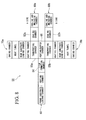
- FIG 4 is a block diagram showing the apparatus for manufacturing a PDP according to the first embodiment of the present invention.
- a rear end of a front substrate line 60, a rear end of a rear substrate line 70, and a front end of a panel formation line 80 are each connected to a transporting chamber 55.
- the PDP manufacturing apparatus 50 continuously performs the tasks within the area 50 which is encompassed by the double-dot chain line in the PDP manufacturing process shown in FIG 3 in a vacuum or in a controlled atmosphere.
- the front substrate line 60 is provided with a loading chamber (i.e., an evacuating chamber) 61 which receives the front substrate 1 having just completed the dielectric layer 13 formation step, a heating chamber 62 which heats the front substrate 1 to approximately 150 to 350°C, a film formation chamber 64 which forms the protective film 14 using an electron beam evaporation method, and a heating/buffer chamber 66 which heats the rear substrate 2 to the same temperature as that to which the front substrate 1 is heated (approximately 380°C).
- a loading chamber i.e., an evacuating chamber
- a heating chamber 62 which heats the front substrate 1 to approximately 150 to 350°C
- a film formation chamber 64 which forms the protective film 14 using an electron beam evaporation method
- a heating/buffer chamber 66 which heats the rear substrate 2 to the same temperature as that to which the front substrate 1 is heated (approximately 380°C).
- address electrodes 11 which are formed from Ag, Cr/Cu/Cr, or A1 are formed (S72).
- a dielectric layer 19 is formed in order to protect the address electrodes 11 (S74).
- partition walls 15 are formed using a sand-blasting method or the like in order to increase the electrical discharge space and the light emission surface area of the phosphors 17 (S75).
- the sand-blasting method involves coating a glass paste being the material for the partition walls 15 onto the substrate, drying the glass paste and then arranging thereon a mask material having a pattern, and then blasting the substrate with a polishing agent such as alumina, glass beads or the like so as to form partition walls 15 having a predetermined shape.
- a polishing agent such as alumina, glass beads or the like so as to form partition walls 15 having a predetermined shape.
- the phosphors 17 are applied using a screen printing method or the like, and are then dried. Thereafter, the dried phosphors 17 are baked at approximately 500°C (S76).
- the sealing material 20 is applied onto the surface of the rear substrate 2 while the rear substrate 2 is being heated (S78).
- the rear substrate line 70 is provided with a baking chamber 72 which receives the rear substrate 2 on which the phosphors 17 have been applied and which bakes the rear substrate 2, and a coating chamber 78 which applies the sealing material 20 onto the surface of the rear substrates 2 as shown in FIG. 4 .
- a heat tunnel 74 and a rear substrate loading chamber 76 are provided between the baking chamber 72 and the coating chamber 78.
- the tunnel 74 and rear substrate loading chamber 76 transport the rear substrate 2 which have been baked in the baking chamber 72 to the coating chamber 78 while maintaining the temperature thereof at 100°C or more so that the rear substrate 2 can be coated in the coating chamber 78 with the sealing material 20.
- the heat tunnel 74 is a substrate transporting chamber which is provided with a heat conservation mechanism for maintaining the temperature of the rear substrate 2 after baking. It is noted that, instead of the heat tunnel 74, it may be possible to transport the rear substrate using a stocker type container. Moreover, the heat tunnel 74 may be provided with an exhaust system in order to conduct atmosphere separation. In the rear substrate loading chamber 76, evacuating is performed while maintaining the temperature of the rear substrate 2 after baking held at 100°C or more. It is noted that the rear substrate 2 may be heated in the rear substrate loading chamber 76.
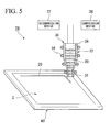
- FIG 5 is a perspective view showing the internal structure of a sealing material coating chamber.
- a hot plate 40 on which is placed a rear substrate 2 to be coated with the sealing material 20 is provided in a bottom portion of the coating chamber 78.
- the hot plate 40 is able to heat the rear substrate 2 to a temperature of approximately 100 to 450°C.
- a heater may be installed to perform radiation heating to the rear substrate 2.
- a dispenser (i.e., a coating device) 30 which discharges the sealing material 20 is provided above the hot plate 40.
- the hot plate 40 may be mounted on an XY stage (not shown) such that the hot plate 40 and dispenser 30 are able to move relatively to each other within a horizontal plane.
- the hot plate 40 is fixed in position and the dispenser 30 is installed on an XY movable mechanism (i.e., a plane scanning mechanism).
- the coating chamber 78 is provided with an evacuation system (not shown) which consists of a turbo-molecular pump and a cold trap for absorbing and discharging moisture.
- a nozzle 31 is fitted onto the distal end of a syringe 32 having cylindrical shape. Sealing material 20 filled inside the syringe 32 is discharged from the distal end of the nozzle 31.
- a heater 34 is provided so as to surround the outer circumference of the syringe 32 and nozzle 31. The sealing material 20 filled inside the dispenser 30 is heated by the heater 34 to greater than or equal to its melting point and is accordingly melted.
- a decompression device 37 such as a vacuum pump and a compression device 38 such as a compressor are connected to a top end of the syringe 32. The decompression device 37 causes gas contained inside melted sealing material 20 to be pumped out therefrom. The compression device 38 causes melted sealing material 20 to be quantitatively discharged from the nozzle 31.
- the interior of the dispenser 30 is filled with the low melting point glass and filler powder which form the sealing material 20.
- electric current is conducted to the heater 34 so that the powder of the sealing material 20 is heated to a higher temperature than or equal to its melting point (i.e., approximately 300 to 480°C).
- the decompression device 37 is driven so that an interior 36 of the syringe 32 is decompressed to approximately 0.1 Pa.
- gas such as H 2 , H 2 O, N 2 , CO, CO 2 , and the like
- low melting point glass and filler may be molded into a cylindrical shape in advance, and then set the molded material in the syringe. In this case, vacuum deaeration processing is performed during the molding or when the molded material is being melted after it has been set in the syringe. Further, low melting point glass and filler, or low melting point glass alone may be melted, deaerated and stirred in advance, and then the resulting material may be supplied to the syringe using a transporting device such as a pipe.
- the interior of the coating chamber 78 is held in a vacuum or in a controlled atmosphere.
- a rear substrate 2 is placed on top of the hot plate 40.
- the hot plate 40 is moved using the XY stage, and the coating start position on the rear substrate 2 where application of the sealing material 20 begins is placed below the dispenser 30.
- the compression device 38 is driven so that the interior of the syringe 32 is compressed to a predetermined pressure. As a result, the melted sealing material 20 is discharged quantitatively from the nozzle 31. In this state, by moving the hot plate 40 using the XY stage, the sealing material 20 can be applied continuously onto peripheral edge portions of the rear substrate 2.
- a panel formation step in which the above described front substrate 1 and rear substrate 2 are laminated together is performed (S80).
- an alignment step (S82) to align the two substrates, and an electrical discharge gas introduction and sealing step (S84) are performed. It is noted that, if necessary, an aging step (S86) is performed for a short period of time.
- the front substrate 1 on which the protective film 14 is formed is heated to approximately 380°C in the heating/buffer chamber
- the front substrate 1 is transported to a sealing chamber 82 via the transporting chamber 55.
- the transported front substrate 1 is held by a hook mechanism provided in a top portion of the sealing chamber 82. While the front substrate 1 is being held, its temperature is maintained at approximately 380°C by a heater placed in the top portion of the sealing chamber 82.
- the rear substrate 2 on which the sealing material 20 is applied is transported from the coating chamber 78 to the sealing chamber 82 via the transporting chamber 55.
- the transported rear substrate 2 is placed on the hot plate provided in a bottom portion of the sealing chamber 82 and is held at approximately 380°C.
- alignment marks on the front substrate 1 and rear substrate 2 are read by a CCD camera installed on the atmosphere side of a vacuum tank provided in the sealing chamber, and the two substrates are positioned relative to each other.
- electrical discharge gas is introduced, pressure is applied to the two substrates, the sealing material is heated to approximately 430 to 450°C, and then sealing is achieved.
- the panel obtained by the sealing is then transported to a cooling/unloading chamber where it is cooled to approximately 150°C and is then unloaded.
- the rear substrate 2 whose phosphors have been baked in the baking chamber 72 is introduced to the sealing chamber 82 via the heat tunnel 74, the rear substrate loading chamber 76, the coating chamber 78, and the transporting chamber 55 while being maintained in a vacuum or in a controlled atmosphere. Namely, it is possible to introduce the rear substrate 2 to the sealing chamber 82 while preventing any impurity gas from adsorbing thereto.
- FIG. 6 is a graph showing measurement results when the quantity of released gas from the sealing material was measured using thermal desorption spectroscopy (TDS).
- TDS thermal desorption spectroscopy
- the temperature of the sealing material is raised to approximately 450°C over approximately 2200 seconds, and is then held in this state.
- the measurement results of the quantity of released gas from a conventional sealing material are shown by a broken line, while the measurement results of the quantity of released gas from the sealing material according to the present invention are shown by a solid line.
- Impurity gas which is absorbed by the coating film on the surface of the substrate is released from the surface of the substrate if the substrate interior is purified by vacuum baking and if voltage is applied between the substrates for a predetermined time (i.e., if aging processing is performed).
- the discharge voltage becomes stable. Therefore, in the conventional technology, purification (i.e., drying) is performed for several hours in the sealing step. It has also been necessary to perform aging processing for between several hours and several tens of hours on panels which have completed the sealing step.
- the inventors of the present invention performed aging experiments on a PDP manufactured according to the conventional method and on a PDP manufactured using the method according to the present embodiment.
- MgO having a film thickness of 800 nm was used for the protective film 14 of the PDP in the experiments, and Ne - 4% Xe was introduced at a pressure of 66.5 kPa as the electrical discharge gas.
- Ne - 4% Xe was introduced at a pressure of 66.5 kPa as the electrical discharge gas.
- the respective manufacturing processes to manufacture a PDP are performed using a variety of different apparatuses.
- a PDP was manufactured after the front substrate 1 which has completed the film formation of the protective film 14 was exposed to air (having a humidity of 50%) for one hour.
- FIG. 7 is a graph showing the results of the aging experiments. It is noted that Vf is the discharge starting voltage, and Vs is the discharge sustaining voltage. In the case of the PDP manufactured using the conventional method including the exposure of the substrate to air, both the discharge starting voltage Vf and the discharge sustaining voltage Vs are higher, and approximately 3 hours are necessary until the voltage stabilizes. In contrast, in the case of PDP manufactured using the method of the present embodiment, both the discharge starting voltage Vf and the discharge sustaining voltage Vs are lower, and the discharge starting voltage Vf stabilizes within approximately one minute while the discharge sustaining voltage Vs is stable from the beginning. From these results, it was confirmed that, by employing the PDP manufacturing method and manufacturing apparatus of the present embodiment, it is possible to shorten the aging time. Moreover, it was confirmed that the discharge voltage is lowered. Namely, by employing the PDP manufacturing method and manufacturing apparatus of the present embodiment, it is possible to provide a PDP having a low level of power consumption.
- the PDP manufacturing method of the present embodiment is provided with a step of melting a sealing material 20 which does not contain any binder for making the sealing material into paste form inside a dispenser, a coating step of applying the melted sealing material 20 onto the surface of a rear substrate 2 using the dispenser, and a sealing step of laminating a front substrate 1 and rear substrate 2 via the sealing material 20 applied onto the surface of the rear substrate 2.
- a sealing material 20 which does not contain any binder is used, by melting the sealing material 20 inside a dispenser, it can be applied onto the surface of a rear substrate 2.
- a sealing material 20 which does not contain any binder is used, it becomes possible to greatly reduce the quantity of released gas from the sealing material 20.
- the PDP manufacturing method of the present embodiment is provided with a step of decompressing the interior of the dispenser prior to the coating step so that any gas contained within the sealing material 20 is released.
- a sealing material 20 from which internal gas has been released is applied, it is possible to even further reduce the quantity of released gas released from the coated sealing material 20.
- the purification (i.e., drying) time required to purify the panel interior in the sealing step or else to eliminate this purification (i.e., drying) altogether.
- FIG. 8 is a block diagram showing a PDP manufacturing apparatus according to a second embodiment.
- one sealing chamber is connected to one film formation chamber.
- a plurality of sealing chambers 82a and 82b are connected to one film formation chamber 64. It is noted that any detailed description of portions which are the same as those in the first embodiment is omitted.
- a transporting chamber 55a is connected to an A side of a heating/buffer chamber 66 on the front substrate line 60, while a transporting chamber 55b is connected to a B side of the heating/buffet chamber 66.
- a rear substrate line 70a and a panel formation line 80a are connected to the A side transporting chamber 55a.
- a rear substrate line 70b and a panel formation line 80b are connected to the B side transporting chamber 55b.
- the sealing chambers 82a and 82b of the rear substrate lines 70a and 70b are connected to the film formation chamber 64 of the front substrate line 60.
- the rear substrate lines 70a and 70b extend perpendicularly to the front substrate line 60, and the panel formation lines 80a and 80b extend parallel with the front substrate line 60.
- the tact time required for the film formation step in the film formation chamber 64 is shorter compared to the tact time required for the panel formation step in the sealing chambers 82a and 82b. Therefore, in the present embodiment, a structure is employed in which a plurality of sealing chambers 82a and 82b are connected to the film formation chamber 64. By employing this structure, it becomes possible to improve the operating efficiency of the film formation chamber. As a result, compared with the first embodiment, it is possible to improve throughput (for example by a factor of approximately 2) in manufacturing PDP.
- the plurality of sealing chambers 82a and 82b may be formed such that the sizes of front substrate 1 and rear substrate 2 laminated together are different between the plurality of sealing chambers. Namely, it is possible to employ a structure in which, in the plurality of sealing chambers 82a and 82b, when manufacturing a plurality of PDPs having mutually different sizes, a front substrate 1 and a rear substrate 2 which correspond to the size of each of the PDPs are laminated together. For example, a structure can be employed in which the sealing of a panel having a diagonal length of 42 inches is performed in the A side sealing chamber 82a, while the sealing of a panel having a diagonal length of 50 inches is performed in the B side sealing chamber 82b.
- the film formation chamber 64 is formed so as to conduct film formation for front substrates of different sizes. As a result, it is possible to efficiently manufacture panels of different sizes. Moreover, when manufacturing panels having mutually different sizes, a portion of the manufacturing apparatus (i.e., the front substrate line including the film formation chamber) can be shared. As a result, manufacturing costs can be reduced.
- FIG 9 is a block diagram showing a PDP manufacturing apparatus according to a variant example of the second embodiment.
- the rear substrate lines 70a and 70b extend perpendicularly to the front substrate line 60
- the panel formation lines 80a and 80b extend parallel with the front substrate line 60.
- the rear substrate lines 70a and 70b extend parallel with the front substrate line 60
- the panel formation lines 80a and 80b extend perpendicularly to the front substrate line 60.
- the present invention is applied to a plasma display panel, however, may be applied to a field emission display panel.
- electrons are emitted from electron emission source (i.e., emitter) provided for every pixel into vacuum, and collided against phosphors, thereby attaining light emission.
- electron emission source i.e., emitter
- field emission display panels include a FED (Field Emission Displays) equipped with projection-shaped electron emission pixels, and a SED (Surface-Conduction Electron-Emitter Displays) equipped with surface conduction-type electron emission pixels. Even in a case where the present invention is applied to these field emission display panels, it is still possible to reduce the aging time, and suppress any rise in the discharge voltage.
Landscapes
- Engineering & Computer Science (AREA)
- Physics & Mathematics (AREA)
- Plasma & Fusion (AREA)
- Manufacturing & Machinery (AREA)
- Manufacture Of Electron Tubes, Discharge Lamp Vessels, Lead-In Wires, And The Like (AREA)
- Gas-Filled Discharge Tubes (AREA)
Applications Claiming Priority (2)
| Application Number | Priority Date | Filing Date | Title |
|---|---|---|---|
| JP2007153291 | 2007-06-08 | ||
| PCT/JP2008/060019 WO2008149804A1 (fr) | 2007-06-08 | 2008-05-30 | Procédé et dispositif de fabrication de panneau d'étanchéité et dispositif de fabrication d'un panneau d'affichage plasma |
Publications (3)
| Publication Number | Publication Date |
|---|---|
| EP2148355A1 true EP2148355A1 (fr) | 2010-01-27 |
| EP2148355A4 EP2148355A4 (fr) | 2011-03-16 |
| EP2148355B1 EP2148355B1 (fr) | 2013-05-29 |
Family
ID=40093622
Family Applications (1)
| Application Number | Title | Priority Date | Filing Date |
|---|---|---|---|
| EP08777030.1A Not-in-force EP2148355B1 (fr) | 2007-06-08 | 2008-05-30 | Procédé et dispositif de fabrication de panneau d'étanchéité et dispositif de fabrication d'un panneau d'affichage plasma |
Country Status (7)
| Country | Link |
|---|---|
| US (1) | US8454404B2 (fr) |
| EP (1) | EP2148355B1 (fr) |
| JP (1) | JP5373605B2 (fr) |
| KR (1) | KR101102494B1 (fr) |
| CN (1) | CN101675492B (fr) |
| RU (1) | RU2435246C2 (fr) |
| WO (1) | WO2008149804A1 (fr) |
Families Citing this family (4)
| Publication number | Priority date | Publication date | Assignee | Title |
|---|---|---|---|---|
| US8956892B2 (en) * | 2012-01-10 | 2015-02-17 | Asm Technology Singapore Pte. Ltd. | Method and apparatus for fabricating a light-emitting diode package |
| TWI549256B (zh) * | 2012-12-24 | 2016-09-11 | 鴻海精密工業股份有限公司 | 發光二極體模組之製造方法 |
| RU2594958C2 (ru) * | 2013-08-07 | 2016-08-20 | Открытое акционерное общество Центральный научно-исследовательский институт "ЦИКЛОН" | Способ герметизации oled и микродисплея oled на кремниевой подложке с помощью стеклообразной пасты |
| TWI530398B (zh) * | 2014-04-29 | 2016-04-21 | 群創光電股份有限公司 | 顯示面板 |
Family Cites Families (19)
| Publication number | Priority date | Publication date | Assignee | Title |
|---|---|---|---|---|
| SU497653A1 (ru) | 1967-11-20 | 1975-12-30 | Предприятие П/Я В-2307 | Способ вакуумноплотного сочленени деталей стеклооболочки цветного кинескопа |
| US4273585A (en) * | 1980-04-21 | 1981-06-16 | Exxon Research & Engineering Co. | Sealing glass |
| US4377404A (en) * | 1980-07-19 | 1983-03-22 | Matsuo Electric Company Limited | Hermetic glass-to-metal seal and method for making same |
| KR100727735B1 (ko) * | 1999-11-11 | 2007-06-13 | 마츠시타 덴끼 산교 가부시키가이샤 | 가스방전패널의 제조방법 및 그 제조장치 |
| CN100336157C (zh) * | 2000-03-31 | 2007-09-05 | 松下电器产业株式会社 | 等离子体显示面板的制造方法 |
| KR100445954B1 (ko) | 2000-08-07 | 2004-08-25 | 미쓰비시덴키 가부시키가이샤 | 평면형 발광 표시 패널의 제조 방법 |
| JP2002075192A (ja) | 2000-08-24 | 2002-03-15 | Matsushita Electric Ind Co Ltd | ガス放電パネルの製造方法およびそれを用いたガス放電パネル |
| JP2002245941A (ja) * | 2001-02-13 | 2002-08-30 | Nec Corp | プラズマディスプレイパネルの製造方法 |
| RU2185678C1 (ru) | 2001-02-27 | 2002-07-20 | Открытое акционерное общество "Научно-исследовательский институт газоразрядных приборов "Плазма" | Газоразрядная индикаторная панель переменного тока |
| JP2002367514A (ja) | 2001-06-12 | 2002-12-20 | Matsushita Electric Ind Co Ltd | 表示パネルおよびその製造方法およびその製造装置 |
| JP4574081B2 (ja) * | 2001-08-09 | 2010-11-04 | キヤノン株式会社 | 画像表示装置の製造方法 |
| JP2003223847A (ja) | 2002-01-30 | 2003-08-08 | Fujitsu Ltd | プラズマディスプレイパネルの背面基板及びその製造方法 |
| JP4261861B2 (ja) * | 2002-09-30 | 2009-04-30 | 双葉電子工業株式会社 | 蛍光表示管用封着材及び蛍光表示管 |
| JP2004146211A (ja) * | 2002-10-24 | 2004-05-20 | Noritake Co Ltd | 平板型表示装置およびその封着方法 |
| US6967441B2 (en) * | 2002-12-31 | 2005-11-22 | Ningbo Tianming Electronic Co. Ltd | Plasma display panel for multi-screen system |
| RU2248062C2 (ru) | 2003-01-08 | 2005-03-10 | Открытое акционерное общество "Научно-исследовательский институт газоразрядных приборов "Плазма" (ОАО "Плазма") | Способ изготовления газоразрядной индикаторной панели переменного тока |
| US6998776B2 (en) * | 2003-04-16 | 2006-02-14 | Corning Incorporated | Glass package that is hermetically sealed with a frit and method of fabrication |
| US7888870B2 (en) * | 2004-12-16 | 2011-02-15 | Panasonic Corporation | Plasma display panel, method of producing the same, and sealing member |
| RU2285974C1 (ru) | 2005-03-21 | 2006-10-20 | Открытое акционерное общество "Научно-исследовательский институт газоразрядных приборов "Плазма" (ОАО "Плазма") | Способ изготовления газоразрядной индикаторной панели переменного тока |
-
2008
- 2008-05-30 WO PCT/JP2008/060019 patent/WO2008149804A1/fr not_active Ceased
- 2008-05-30 EP EP08777030.1A patent/EP2148355B1/fr not_active Not-in-force
- 2008-05-30 JP JP2009517841A patent/JP5373605B2/ja not_active Expired - Fee Related
- 2008-05-30 KR KR1020097023286A patent/KR101102494B1/ko not_active Expired - Fee Related
- 2008-05-30 CN CN2008800150425A patent/CN101675492B/zh not_active Expired - Fee Related
- 2008-05-30 RU RU2009144978/07A patent/RU2435246C2/ru not_active IP Right Cessation
- 2008-05-30 US US12/601,097 patent/US8454404B2/en not_active Expired - Fee Related
Non-Patent Citations (2)
| Title |
|---|
| No further relevant documents disclosed * |
| See also references of WO2008149804A1 * |
Also Published As
| Publication number | Publication date |
|---|---|
| KR101102494B1 (ko) | 2012-01-05 |
| KR20090129510A (ko) | 2009-12-16 |
| EP2148355A4 (fr) | 2011-03-16 |
| RU2009144978A (ru) | 2011-06-10 |
| US20100159787A1 (en) | 2010-06-24 |
| JP5373605B2 (ja) | 2013-12-18 |
| CN101675492B (zh) | 2011-12-21 |
| CN101675492A (zh) | 2010-03-17 |
| JPWO2008149804A1 (ja) | 2010-08-26 |
| EP2148355B1 (fr) | 2013-05-29 |
| WO2008149804A1 (fr) | 2008-12-11 |
| RU2435246C2 (ru) | 2011-11-27 |
| US8454404B2 (en) | 2013-06-04 |
Similar Documents
| Publication | Publication Date | Title |
|---|---|---|
| US6984159B1 (en) | Plasma display panel with superior light-emitting characteristics, and method and apparatus for producing the plasma display panel | |
| KR100827504B1 (ko) | 플라즈마 디스플레이 패널의 제조방법 | |
| KR100723752B1 (ko) | 발광특성이 뛰어난 플라즈마 디스플레이 패널의 제조방법 | |
| EP2148355B1 (fr) | Procédé et dispositif de fabrication de panneau d'étanchéité et dispositif de fabrication d'un panneau d'affichage plasma | |
| US8460048B2 (en) | Method and apparatus for manufacturing plasma display panel | |
| JP2001035372A (ja) | プラズマディスプレイパネル、その製造方法及び製造装置 | |
| JP3553903B2 (ja) | プラズマディスプレイパネルの製造方法 | |
| JP2002334656A (ja) | プラズマディスプレイおよびその製造方法 | |
| JP3420218B2 (ja) | プラズマディスプレイパネルの製造方法 | |
| JP2009163980A (ja) | 封着パネルの製造方法及びそれを用いたプラズマディスプレイパネルの製造方法、紫外線硬化性樹脂 | |
| JP3553902B2 (ja) | プラズマディスプレイパネルの製造方法及び製造装置 | |
| JP3540764B2 (ja) | プラズマディスプレイパネル | |
| JP3374789B2 (ja) | プラズマディスプレイパネルおよびその製造方法 | |
| JP2009093951A (ja) | 封着パネルの製造方法及びそれを用いたプラズマディスプレイパネルの製造方法 | |
| JP2002075217A (ja) | プラズマディスプレイ用部材およびプラズマディスプレイならびにその製造方法 | |
| JP2001351532A (ja) | プラズマディスプレイパネル | |
| JP2002140983A (ja) | パネル保護基板を使用した表示パネルの製造方法および製造装置 | |
| JP2002075211A (ja) | ガス放電パネル及びその製造方法 | |
| JP2001351523A (ja) | プラズマディスプレイパネルの製造方法及び製造装置 | |
| JP2002140987A (ja) | プラズマディスプレイパネルおよびその製造方法 | |
| JP2002117765A (ja) | 画像表示装置の製造方法およびそれを用いて製造した画像表示装置 | |
| JP2004335403A (ja) | 蛍光体処理装置と処理方法 | |
| KR20060106500A (ko) | 플라즈마 디스플레이 패널 및 그의 제조방법 | |
| JP2002075194A (ja) | プラズマディスプレイパネルおよびその製造方法 | |
| CN102449722A (zh) | 等离子显示面板的制造方法 |
Legal Events
| Date | Code | Title | Description |
|---|---|---|---|
| PUAI | Public reference made under article 153(3) epc to a published international application that has entered the european phase |
Free format text: ORIGINAL CODE: 0009012 |
|
| 17P | Request for examination filed |
Effective date: 20091215 |
|
| AK | Designated contracting states |
Kind code of ref document: A1 Designated state(s): AT BE BG CH CY CZ DE DK EE ES FI FR GB GR HR HU IE IS IT LI LT LU LV MC MT NL NO PL PT RO SE SI SK TR |
|
| AX | Request for extension of the european patent |
Extension state: AL BA MK RS |
|
| DAX | Request for extension of the european patent (deleted) | ||
| A4 | Supplementary search report drawn up and despatched |
Effective date: 20110216 |
|
| 17Q | First examination report despatched |
Effective date: 20111005 |
|
| GRAP | Despatch of communication of intention to grant a patent |
Free format text: ORIGINAL CODE: EPIDOSNIGR1 |
|
| RIC1 | Information provided on ipc code assigned before grant |
Ipc: H01J 9/26 20060101AFI20121219BHEP Ipc: H01J 11/12 20120101ALI20121219BHEP Ipc: H01J 11/48 20120101ALI20121219BHEP |
|
| GRAS | Grant fee paid |
Free format text: ORIGINAL CODE: EPIDOSNIGR3 |
|
| GRAA | (expected) grant |
Free format text: ORIGINAL CODE: 0009210 |
|
| RIN1 | Information on inventor provided before grant (corrected) |
Inventor name: YANO, TAKANOBU Inventor name: HAKOMORI, MUNETO Inventor name: IIJIMA, EIICHI Inventor name: KURAUCHI, TOSHIHARU Inventor name: ORII, YUICHI |
|
| AK | Designated contracting states |
Kind code of ref document: B1 Designated state(s): AT BE BG CH CY CZ DE DK EE ES FI FR GB GR HR HU IE IS IT LI LT LU LV MC MT NL NO PL PT RO SE SI SK TR |
|
| REG | Reference to a national code |
Ref country code: GB Ref legal event code: FG4D |
|
| REG | Reference to a national code |
Ref country code: CH Ref legal event code: EP |
|
| REG | Reference to a national code |
Ref country code: AT Ref legal event code: REF Ref document number: 614871 Country of ref document: AT Kind code of ref document: T Effective date: 20130615 |
|
| REG | Reference to a national code |
Ref country code: IE Ref legal event code: FG4D |
|
| REG | Reference to a national code |
Ref country code: DE Ref legal event code: R096 Ref document number: 602008025033 Country of ref document: DE Effective date: 20130725 |
|
| REG | Reference to a national code |
Ref country code: CH Ref legal event code: NV Representative=s name: WAGNER PATENT AG, CH |
|
| REG | Reference to a national code |
Ref country code: AT Ref legal event code: MK05 Ref document number: 614871 Country of ref document: AT Kind code of ref document: T Effective date: 20130529 |
|
| REG | Reference to a national code |
Ref country code: LT Ref legal event code: MG4D |
|
| PG25 | Lapsed in a contracting state [announced via postgrant information from national office to epo] |
Ref country code: SE Free format text: LAPSE BECAUSE OF FAILURE TO SUBMIT A TRANSLATION OF THE DESCRIPTION OR TO PAY THE FEE WITHIN THE PRESCRIBED TIME-LIMIT Effective date: 20130529 Ref country code: AT Free format text: LAPSE BECAUSE OF FAILURE TO SUBMIT A TRANSLATION OF THE DESCRIPTION OR TO PAY THE FEE WITHIN THE PRESCRIBED TIME-LIMIT Effective date: 20130529 Ref country code: SI Free format text: LAPSE BECAUSE OF FAILURE TO SUBMIT A TRANSLATION OF THE DESCRIPTION OR TO PAY THE FEE WITHIN THE PRESCRIBED TIME-LIMIT Effective date: 20130529 Ref country code: GR Free format text: LAPSE BECAUSE OF FAILURE TO SUBMIT A TRANSLATION OF THE DESCRIPTION OR TO PAY THE FEE WITHIN THE PRESCRIBED TIME-LIMIT Effective date: 20130830 Ref country code: FI Free format text: LAPSE BECAUSE OF FAILURE TO SUBMIT A TRANSLATION OF THE DESCRIPTION OR TO PAY THE FEE WITHIN THE PRESCRIBED TIME-LIMIT Effective date: 20130529 Ref country code: IS Free format text: LAPSE BECAUSE OF FAILURE TO SUBMIT A TRANSLATION OF THE DESCRIPTION OR TO PAY THE FEE WITHIN THE PRESCRIBED TIME-LIMIT Effective date: 20130929 Ref country code: PT Free format text: LAPSE BECAUSE OF FAILURE TO SUBMIT A TRANSLATION OF THE DESCRIPTION OR TO PAY THE FEE WITHIN THE PRESCRIBED TIME-LIMIT Effective date: 20130930 Ref country code: ES Free format text: LAPSE BECAUSE OF FAILURE TO SUBMIT A TRANSLATION OF THE DESCRIPTION OR TO PAY THE FEE WITHIN THE PRESCRIBED TIME-LIMIT Effective date: 20130909 Ref country code: LT Free format text: LAPSE BECAUSE OF FAILURE TO SUBMIT A TRANSLATION OF THE DESCRIPTION OR TO PAY THE FEE WITHIN THE PRESCRIBED TIME-LIMIT Effective date: 20130529 Ref country code: NO Free format text: LAPSE BECAUSE OF FAILURE TO SUBMIT A TRANSLATION OF THE DESCRIPTION OR TO PAY THE FEE WITHIN THE PRESCRIBED TIME-LIMIT Effective date: 20130829 |
|
| REG | Reference to a national code |
Ref country code: NL Ref legal event code: VDEP Effective date: 20130529 |
|
| PG25 | Lapsed in a contracting state [announced via postgrant information from national office to epo] |
Ref country code: HR Free format text: LAPSE BECAUSE OF FAILURE TO SUBMIT A TRANSLATION OF THE DESCRIPTION OR TO PAY THE FEE WITHIN THE PRESCRIBED TIME-LIMIT Effective date: 20130529 Ref country code: PL Free format text: LAPSE BECAUSE OF FAILURE TO SUBMIT A TRANSLATION OF THE DESCRIPTION OR TO PAY THE FEE WITHIN THE PRESCRIBED TIME-LIMIT Effective date: 20130529 Ref country code: BG Free format text: LAPSE BECAUSE OF FAILURE TO SUBMIT A TRANSLATION OF THE DESCRIPTION OR TO PAY THE FEE WITHIN THE PRESCRIBED TIME-LIMIT Effective date: 20130829 |
|
| PG25 | Lapsed in a contracting state [announced via postgrant information from national office to epo] |
Ref country code: LV Free format text: LAPSE BECAUSE OF FAILURE TO SUBMIT A TRANSLATION OF THE DESCRIPTION OR TO PAY THE FEE WITHIN THE PRESCRIBED TIME-LIMIT Effective date: 20130529 |
|
| PG25 | Lapsed in a contracting state [announced via postgrant information from national office to epo] |
Ref country code: CZ Free format text: LAPSE BECAUSE OF FAILURE TO SUBMIT A TRANSLATION OF THE DESCRIPTION OR TO PAY THE FEE WITHIN THE PRESCRIBED TIME-LIMIT Effective date: 20130529 Ref country code: BE Free format text: LAPSE BECAUSE OF FAILURE TO SUBMIT A TRANSLATION OF THE DESCRIPTION OR TO PAY THE FEE WITHIN THE PRESCRIBED TIME-LIMIT Effective date: 20130529 Ref country code: EE Free format text: LAPSE BECAUSE OF FAILURE TO SUBMIT A TRANSLATION OF THE DESCRIPTION OR TO PAY THE FEE WITHIN THE PRESCRIBED TIME-LIMIT Effective date: 20130529 Ref country code: DK Free format text: LAPSE BECAUSE OF FAILURE TO SUBMIT A TRANSLATION OF THE DESCRIPTION OR TO PAY THE FEE WITHIN THE PRESCRIBED TIME-LIMIT Effective date: 20130529 Ref country code: SK Free format text: LAPSE BECAUSE OF FAILURE TO SUBMIT A TRANSLATION OF THE DESCRIPTION OR TO PAY THE FEE WITHIN THE PRESCRIBED TIME-LIMIT Effective date: 20130529 |
|
| REG | Reference to a national code |
Ref country code: IE Ref legal event code: MM4A |
|
| PG25 | Lapsed in a contracting state [announced via postgrant information from national office to epo] |
Ref country code: RO Free format text: LAPSE BECAUSE OF FAILURE TO SUBMIT A TRANSLATION OF THE DESCRIPTION OR TO PAY THE FEE WITHIN THE PRESCRIBED TIME-LIMIT Effective date: 20130529 Ref country code: MC Free format text: LAPSE BECAUSE OF FAILURE TO SUBMIT A TRANSLATION OF THE DESCRIPTION OR TO PAY THE FEE WITHIN THE PRESCRIBED TIME-LIMIT Effective date: 20130529 Ref country code: NL Free format text: LAPSE BECAUSE OF FAILURE TO SUBMIT A TRANSLATION OF THE DESCRIPTION OR TO PAY THE FEE WITHIN THE PRESCRIBED TIME-LIMIT Effective date: 20130529 |
|
| REG | Reference to a national code |
Ref country code: CH Ref legal event code: PCAR Free format text: NEW ADDRESS: BAECHERSTRASSE 9, 8832 WOLLERAU (CH) |
|
| PLBE | No opposition filed within time limit |
Free format text: ORIGINAL CODE: 0009261 |
|
| STAA | Information on the status of an ep patent application or granted ep patent |
Free format text: STATUS: NO OPPOSITION FILED WITHIN TIME LIMIT |
|
| GBPC | Gb: european patent ceased through non-payment of renewal fee |
Effective date: 20130829 |
|
| PG25 | Lapsed in a contracting state [announced via postgrant information from national office to epo] |
Ref country code: IE Free format text: LAPSE BECAUSE OF NON-PAYMENT OF DUE FEES Effective date: 20130530 |
|
| 26N | No opposition filed |
Effective date: 20140303 |
|
| REG | Reference to a national code |
Ref country code: FR Ref legal event code: ST Effective date: 20140414 |
|
| REG | Reference to a national code |
Ref country code: DE Ref legal event code: R097 Ref document number: 602008025033 Country of ref document: DE Effective date: 20140303 |
|
| PG25 | Lapsed in a contracting state [announced via postgrant information from national office to epo] |
Ref country code: GB Free format text: LAPSE BECAUSE OF NON-PAYMENT OF DUE FEES Effective date: 20130829 |
|
| PG25 | Lapsed in a contracting state [announced via postgrant information from national office to epo] |
Ref country code: FR Free format text: LAPSE BECAUSE OF NON-PAYMENT OF DUE FEES Effective date: 20130729 |
|
| PG25 | Lapsed in a contracting state [announced via postgrant information from national office to epo] |
Ref country code: MT Free format text: LAPSE BECAUSE OF FAILURE TO SUBMIT A TRANSLATION OF THE DESCRIPTION OR TO PAY THE FEE WITHIN THE PRESCRIBED TIME-LIMIT Effective date: 20130529 |
|
| PG25 | Lapsed in a contracting state [announced via postgrant information from national office to epo] |
Ref country code: TR Free format text: LAPSE BECAUSE OF FAILURE TO SUBMIT A TRANSLATION OF THE DESCRIPTION OR TO PAY THE FEE WITHIN THE PRESCRIBED TIME-LIMIT Effective date: 20130529 Ref country code: CY Free format text: LAPSE BECAUSE OF FAILURE TO SUBMIT A TRANSLATION OF THE DESCRIPTION OR TO PAY THE FEE WITHIN THE PRESCRIBED TIME-LIMIT Effective date: 20130529 |
|
| PG25 | Lapsed in a contracting state [announced via postgrant information from national office to epo] |
Ref country code: HU Free format text: LAPSE BECAUSE OF FAILURE TO SUBMIT A TRANSLATION OF THE DESCRIPTION OR TO PAY THE FEE WITHIN THE PRESCRIBED TIME-LIMIT; INVALID AB INITIO Effective date: 20080530 Ref country code: LU Free format text: LAPSE BECAUSE OF NON-PAYMENT OF DUE FEES Effective date: 20130530 |
|
| PGFP | Annual fee paid to national office [announced via postgrant information from national office to epo] |
Ref country code: DE Payment date: 20190521 Year of fee payment: 12 Ref country code: IT Payment date: 20190527 Year of fee payment: 12 |
|
| PGFP | Annual fee paid to national office [announced via postgrant information from national office to epo] |
Ref country code: CH Payment date: 20190521 Year of fee payment: 12 |
|
| REG | Reference to a national code |
Ref country code: DE Ref legal event code: R119 Ref document number: 602008025033 Country of ref document: DE |
|
| PG25 | Lapsed in a contracting state [announced via postgrant information from national office to epo] |
Ref country code: CH Free format text: LAPSE BECAUSE OF NON-PAYMENT OF DUE FEES Effective date: 20200531 Ref country code: LI Free format text: LAPSE BECAUSE OF NON-PAYMENT OF DUE FEES Effective date: 20200531 |
|
| PG25 | Lapsed in a contracting state [announced via postgrant information from national office to epo] |
Ref country code: DE Free format text: LAPSE BECAUSE OF NON-PAYMENT OF DUE FEES Effective date: 20201201 |
|
| PG25 | Lapsed in a contracting state [announced via postgrant information from national office to epo] |
Ref country code: IT Free format text: LAPSE BECAUSE OF NON-PAYMENT OF DUE FEES Effective date: 20200530 |