EP2148371B1 - Organische lichtemittierende Anzeigevorrichtung - Google Patents
Organische lichtemittierende Anzeigevorrichtung Download PDFInfo
- Publication number
- EP2148371B1 EP2148371B1 EP09251834.9A EP09251834A EP2148371B1 EP 2148371 B1 EP2148371 B1 EP 2148371B1 EP 09251834 A EP09251834 A EP 09251834A EP 2148371 B1 EP2148371 B1 EP 2148371B1
- Authority
- EP
- European Patent Office
- Prior art keywords
- wires
- pixel region
- electrodes
- organic light
- display device
- Prior art date
- Legal status (The legal status is an assumption and is not a legal conclusion. Google has not performed a legal analysis and makes no representation as to the accuracy of the status listed.)
- Not-in-force
Links
Images

Classifications
-
- H—ELECTRICITY
- H10—SEMICONDUCTOR DEVICES; ELECTRIC SOLID-STATE DEVICES NOT OTHERWISE PROVIDED FOR
- H10K—ORGANIC ELECTRIC SOLID-STATE DEVICES
- H10K59/00—Integrated devices, or assemblies of multiple devices, comprising at least one organic light-emitting element covered by group H10K50/00
- H10K59/10—OLED displays
- H10K59/17—Passive-matrix OLED displays
- H10K59/173—Passive-matrix OLED displays comprising banks or shadow masks
-
- H—ELECTRICITY
- H10—SEMICONDUCTOR DEVICES; ELECTRIC SOLID-STATE DEVICES NOT OTHERWISE PROVIDED FOR
- H10K—ORGANIC ELECTRIC SOLID-STATE DEVICES
- H10K59/00—Integrated devices, or assemblies of multiple devices, comprising at least one organic light-emitting element covered by group H10K50/00
- H10K59/10—OLED displays
- H10K59/12—Active-matrix OLED [AMOLED] displays
- H10K59/125—Active-matrix OLED [AMOLED] displays including organic TFTs [OTFT]
-
- H—ELECTRICITY
- H10—SEMICONDUCTOR DEVICES; ELECTRIC SOLID-STATE DEVICES NOT OTHERWISE PROVIDED FOR
- H10K—ORGANIC ELECTRIC SOLID-STATE DEVICES
- H10K30/00—Organic devices sensitive to infrared radiation, light, electromagnetic radiation of shorter wavelength or corpuscular radiation
- H10K30/80—Constructional details
- H10K30/81—Electrodes
- H10K30/82—Transparent electrodes, e.g. indium tin oxide [ITO] electrodes
-
- H—ELECTRICITY
- H10—SEMICONDUCTOR DEVICES; ELECTRIC SOLID-STATE DEVICES NOT OTHERWISE PROVIDED FOR
- H10K—ORGANIC ELECTRIC SOLID-STATE DEVICES
- H10K71/00—Manufacture or treatment specially adapted for the organic devices covered by this subclass
- H10K71/70—Testing, e.g. accelerated lifetime tests
-
- Y—GENERAL TAGGING OF NEW TECHNOLOGICAL DEVELOPMENTS; GENERAL TAGGING OF CROSS-SECTIONAL TECHNOLOGIES SPANNING OVER SEVERAL SECTIONS OF THE IPC; TECHNICAL SUBJECTS COVERED BY FORMER USPC CROSS-REFERENCE ART COLLECTIONS [XRACs] AND DIGESTS
- Y02—TECHNOLOGIES OR APPLICATIONS FOR MITIGATION OR ADAPTATION AGAINST CLIMATE CHANGE
- Y02E—REDUCTION OF GREENHOUSE GAS [GHG] EMISSIONS, RELATED TO ENERGY GENERATION, TRANSMISSION OR DISTRIBUTION
- Y02E10/00—Energy generation through renewable energy sources
- Y02E10/50—Photovoltaic [PV] energy
- Y02E10/549—Organic PV cells
-
- Y—GENERAL TAGGING OF NEW TECHNOLOGICAL DEVELOPMENTS; GENERAL TAGGING OF CROSS-SECTIONAL TECHNOLOGIES SPANNING OVER SEVERAL SECTIONS OF THE IPC; TECHNICAL SUBJECTS COVERED BY FORMER USPC CROSS-REFERENCE ART COLLECTIONS [XRACs] AND DIGESTS
- Y02—TECHNOLOGIES OR APPLICATIONS FOR MITIGATION OR ADAPTATION AGAINST CLIMATE CHANGE
- Y02P—CLIMATE CHANGE MITIGATION TECHNOLOGIES IN THE PRODUCTION OR PROCESSING OF GOODS
- Y02P70/00—Climate change mitigation technologies in the production process for final industrial or consumer products
- Y02P70/50—Manufacturing or production processes characterised by the final manufactured product
Definitions
- aspects of the present invention relate to an organic light-emitting display device.
- An organic light-emitting display device is a self-emissive, next-generation, display device that has an improved viewing angle, contrast, response time, and power consumption, as compared to a liquid crystal display device (LCD).
- An organic light-emitting display device can be a passive-matrix, organic light-emitting display device, where pixels are coupled in a matrix between scan lines and signal lines, or an active-matrix, organic light-emitting display device, where pixels are controlled by thin film transistors (TFT).
- TFT thin film transistors
- the organic light-emitting diodes constituting a pixel are each composed of an anode electrode, an organic thin film layer, and a cathode electrode.
- a predetermined voltage is applied between the anode electrode and the cathode electrode, holes injected through the anode electrode are recombined with electrons injected through the cathode electrode, to form excitons in a light-emitting layer. Photons are emitted when the excitons return to a lower energy state.
- pixels are tested using a lightening test and an aging test, during the manufacture of an organic light-emitting display device.
- a short bar is used to supply a constant test signal to scan lines or signal lines.
- Korean Patent Publication No. 2006-29086 (April 04, 2006 ) and Korean Patent Publication No. 2006-127561 (December 13, 2006 ) disclose a positive short bar and a negative short bar, which are formed in a data pad that is coupled to data lines and a scan pad that is coupled to scan lines.
- the lightening test is carried out when a test pin is in contact with the short bar.
- the short bars are removed during a scribing procedure, which involves cutting a substrate when the lightening test is completed.
- EP 1 648 033 discloses an organic light emitting display device in accordance with the precharacterising portion of appended claim 1.
- EP 1 850 390 discloses a configuration of an organic light emitting display device in which an insulating layer is formed on the substrate covering both the data lines and the scan lines, wherein the insulating layer has openings corresponding to connecting portions and of the data lines and scan lines respectively.
- An aspect of the present invention provides an organic light-emitting display device, in which a short bar can be easily formed and removed, in order to perform a lightening test and an aging test.
- the organic light-emitting display device includes a drive circuit that is mounted on a substrate.
- Another aspect of the present invention provides an organic light-emitting display device, in which a short bar can be easily formed and removed, in order to perform a lightening test and an aging test.
- the organic light-emitting display device includes auxiliary electrodes to reduce the resistance of scan lines and data lines.
- an organic light-emitting display device as set out in claim 1.
- Preferred features of this aspect are set out in claims 2 to 8.
- first element when a first element is referred to as being formed or disposed "on" another element, the first element can directly contact the second element, or one or more intervening elements can be interposed therebetween. Also, when a first element is referred to as being "connected to" a second element, the first element can be directly connected to the second element, or can be connected to the second element with one or more intervening elements.
- FIG. 1 and FIG. 2 are a plane view and a cross-sectional view, respectively, showing an organic light-emitting display device, according to one embodiment of the present invention.
- FIG. 2 schematically shows section I1 - I2 of FIG. 1 .
- the organic light-emitting display device includes substrate 100, which can be made of an insulating material, such as glass or plastic, or can be made of a metal.
- the substrate 100 is divided into a pixel region 20 and a non-pixel region 40.
- the non-pixel region 40 is disposed around the pixel region 20.
- An array of organic light-emitting diodes 110 are coupled between a matrix of anode electrodes 12 and cathode electrodes 14, in the pixel region 20 of the substrate 100.
- Data lines 62 and scan lines 64 are respectively connected to the anode electrodes 12 and cathode electrodes 14, and are disposed in the non-pixel region 40.
- a power supply line (not shown) supplies a driving voltage to the organic light-emitting diodes 110, and a drive circuit 90 processes external signals supplied through an input pad 66.
- the power supply line, drive circuit 90, and the input pad 66 are disposed in the non-pixel region 40.
- the organic light-emitting diodes 110 each include a portion of one of the anode electrodes 12 and a portion of one of the cathode electrodes 14, which intersect one another, and a portion of an organic thin film layer (not shown) that is disposed therebetween.
- the organic thin film layer includes a hole transport layer, an organic light-emitting layer, and an electron transport layer, and may further include a hole injection layer and an electron injection layer.
- the drive circuit 90 may be formed on the non-pixel region 40 and coupled to data lines 62 and scan lines 64.
- the drive circuit 90 may alternatively be an integrated circuit semiconductor chip that is mounted on the substrate 100, by a chip on glass or wire bonding process.
- a passivation layer 80 covers the pixel region 20 and the non-pixel region 40, and is made of a polyimide-based, a phenol resin-based, or an acrylic resin-based, insulating material.
- the passivation layer 80 includes openings 80a-80c.
- the openings 80a and 80b respectively expose an input pad 66 and a region where the drive circuit 90 is mounted.
- the opening 80c exposes some of the scan lines 64.
- the opening 80c is a region in which a short bar, to commonly couple the data lines 62 or the scan lines 64, is formed. The short bar is used to perform a lightening test and/or an aging test.
- the position of the opening 80c may be suitably selected for minimal size.
- the opening 80c is shown to expose the scan lines 64, but may also be positioned to expose the data lines 62.
- the passivation layer 80 may include another opening to expose the data lines 62.
- the passivation layer 80 may include two openings 80c, each of which exposes about half of the scan lines 64 or data lines 62, for example.
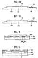
- FIG. 3A and FIG. 3B are cross-sectional views showing a cross-section taken along line I11 - 112 of FIG. 1 .
- FIG. 3A shows that the opening 80c is formed in the passivation layer 80
- FIG. 3B shows a short bar 400 disposed in the opening 80c and commonly coupled to the scan lines 64.
- a test signal is supplied to the organic light-emitting diodes 110, via the data lines 62 or the scan lines 64.
- a test pin is brought into contact with the short bar 400, so as to perform a lightening test and an aging test.
- the short bar 400 is removed.
- the short bar 400 is generally formed of a metal such as aluminum (Al), which may be removed by an acid solution, or the like.
- Al aluminum
- the passivation layer 80 covers the entire surface of the substrate 100, the data lines 62 and the scan lines 64 are protected, when the substrate 100 is dipped into the acid solution.
- the short bar 400 is commonly coupled to some of the scan lines 64, via the opening 80c.
- the opening 80c can include a plurality of openings formed in the passivation layer 80, to expose each of the scan lines 64.
- the short bar 400 is commonly coupled to the scan lines 64 through the plurality of openings, as shown in FIG. 4 .
- the data lines 62 and the scan lines 64 may be made of a transparent electrode material selected from the group consisting of indium tin oxide (ITO), indium zinc oxide (IZO), and indium tin zinc oxide (ITZO). Since the transparent electrode material has a high resistance, the data lines 62 and the scan lines 64 can include a auxiliary electrodes that are formed of a material having a low resistance, so as to reduce the resistance of the data lines 62 and the scan lines 64.
- the scan lines 64 may include transparent electrodes 64a and auxiliary electrodes 64b, as shown in FIG. 4 .
- the auxiliary electrodes 64b may be made of a metal, such as aluminum (Al), silver (Ag), molybdenum (Mo), copper (Cu) chromium (Cr), or multiple layers thereof.
- the auxiliary electrode 64b may include multiple layers of molybdenum (Mo), aluminum (Al), and/or molybdenum (Mo).
- An encapsulation substrate 200 is disposed on the substrate 100, in order to encapsulate the organic light-emitting diodes 100.
- the substrate 100 and the encapsulation substrate 200 are attached to each other by a sealant 300, such as an epoxy, frit seal, or the like.
- the organic light-emitting display device includes the passivation layer 80 formed on the substrate 100.
- the passivation layer 80 includes the opening 80c to expose some of the data lines 62 and/or the scan lines 64.
- the passivation layer 80 may cover the pixel region 20 and the non-pixel region 40, as shown in FIG. 3A and FIG. 3B .
- the passivation layer 80 may disposed between the anode electrodes 12 and the cathode electrodes 14.
- FIG. 5 is a cross-sectional view showing a passivation layer 80 disposed between an anode electrode 12 and a cathode electrode 14, according to an embodiment of the present invention.
- FIG. 5 cross-sectional view showing a portion of the pixel region 20, taken along linel 1 - 12 of FIG. 1 .
- the anode electrode 12 is formed on the pixel region 20 in one direction, and the data lines 62 extended from the anode electrode 12.
- the scan lines 64 are coupled to the cathode electrodes 14 and are formed in the non-pixel region 40.
- the data lines 62 and the scan lines 64 both comprise auxiliary electrodes and transparent electrodes that are formed on the auxiliary electrodes.
- a passivation layer 80 covers the pixel region 20 and the non-pixel region 40, and is patterned to expose the anode electrodes 12.
- the openings 80a and 80b expose an input pad 66 and a region where the drive circuit 90 is mounted, respectively.
- Openings 80c expose the data lines 62.
- the scan lines 64 are formed on the passivation layer 80.
- a barrier rib (not shown) is formed on the passivation layer 80 in the pixel region 20 and extends across the anode electrodes 12.
- the barrier rib separates the cathode electrodes 12 and an organic thin film layer that is on the passivation layer 80.
- the walls of the barrier rib are tapered, such that they have a maximum thickness at the passivation layer 80.
- the cathode electrodes 14 are formed across the anode electrodes 12.
- a short bar 400 may be formed during the formation of the cathode electrodes 14.
Landscapes
- Engineering & Computer Science (AREA)
- Physics & Mathematics (AREA)
- Electromagnetism (AREA)
- Microelectronics & Electronic Packaging (AREA)
- Manufacturing & Machinery (AREA)
- Electroluminescent Light Sources (AREA)
- Devices For Indicating Variable Information By Combining Individual Elements (AREA)
Claims (14)
- Organische Lichtemitteranzeigevorrichtung, umfassend:ein Substrat (100) mit einem Bildpunktbereich (20) und einem bildpunktlosen Bereich (40), der einen Ansteuerungsschaltungsmontagebereich aufweist;eine Vielzahl von ersten Elektroden (12, 14), die im Bildpunktbereich angeordnet sind und sich in einer ersten Richtung erstrecken;eine Vielzahl von ersten Leitungen (62, 64), die mit den ersten Elektroden gekoppelt und im bildpunktlosen Bereich angeordnet sind;eine Vielzahl von zweiten Elektroden (14, 12), die im Bildpunktbereich angeordnet sind und sich in einer zweiten Richtung erstrecken;eine Vielzahl von zweiten Leitungen (64, 62), die mit den zweiten Elektroden gekoppelt und im bildpunktlosen Bereich angeordnet sind;eine organische Dünnschicht (13), die zwischen den ersten und zweiten Elektroden angeordnet ist;eine Ansteuerungsschaltung (90), die im Ansteuerungsschaltungsmontagebereich montiert und mit den ersten und zweiten Leitungen gekoppelt ist; undeine auf dem Substrat ausgebildete Passivierungsschicht (80) mit einer Öffnung (80a, 80c), die dafür konfiguriert ist, die ersten Leitungen freizulegen, wobei die Öffnung zwischen dem Ansteuerungsschaltungsmontagebereich und dem Bildpunktbereich positioniert ist;gekennzeichnet durch eine Kurzschlussschiene, die in der Öffnung angeordnet und mit den ersten Leitungen verbunden ist, um die ersten Leitungen gemeinsam zu koppeln.
- Organische Lichtemitteranzeigevorrichtung nach Anspruch 1, worin die ersten Leitungen und die zweiten Leitungen jeweils eine transparente Elektrode und eine auf der transparenten Elektrode angeordnete Hilfselektrode umfassen.
- Organische Lichtemitteranzeigevorrichtung nach Anspruch 2, worin:die transparenten Elektroden ein Material umfassen, das aus der Gruppe ausgewählt wird, die aus Indium-Zinn-Oxid (ITO), Indium-Zink-Oxid (IZO) und Indium-Zinn-Zink-Oxid (ITZO) besteht; unddie Hilfselektroden ein Material umfassen, das aus der Gruppe ausgewählt wird, die aus Aluminium (Al), Silber (Ag), Molybdän (Mo), Kupfer (Cu) und Chrom (Cr) besteht.
- Organische Lichtemitteranzeigevorrichtung nach Anspruch 2, worin die Hilfselektroden zwei oder mehr Schichten umfassen, die jeweils ein Metall umfassen, das unabhängig aus der Gruppe ausgewählt wird, die aus Aluminium (Al), Silber (Ag), Molybdän (Mo), Kupfer (Cu) und Chrom (Cr) besteht.
- Organische Lichtemitteranzeigevorrichtung nach einem der Ansprüche 1 bis 4, worin die Passivierungsschicht (80) ein Material umfasst, das aus der Gruppe ausgewählt wird, die aus einem Polyimid, einem Phenolharz und einem Acrylharz besteht.
- Organische Lichtemitteranzeigevorrichtung nach einem der Ansprüche 1 bis 5, worin die Passivierungsschicht zwischen der ersten Elektrode und der zweiten Elektrode angeordnet ist.
- Organische Lichtemitteranzeigevorrichtung nach einem der Ansprüche 1 bis 6, ferner eine Eingangskontaktfläche (66) umfassend, die im bildpunktlosen Bereich (40) ausgebildet, mit einem Eingangsanschluss der Ansteuerungsschaltung (90) gekoppelt und durch eine in der Passivierungsschicht ausgebildete zweite Öffnung (80b) freigelegt ist.
- Organische Lichtemitteranzeigevorrichtung nach einem der Ansprüche 1 bis 7;
worin die ersten Leitungen die einen von entweder Rasterleitungen oder Datenleitungen bilden und die zweiten Leitungen die anderen von entweder Rasterleitungen oder Datenleitungen bilden, worin die Passivierungsschicht mindestens eine Öffnung hat, um die Rasterleitungen oder die Datenleitungen mit einer Kurzschlussschiene zu verbinden. - Verfahren zum Herstellen einer organischen Lichtemitteranzeigevorrichtung, umfassend:Ausbilden eines Substrats (100) mit einem Bildpunktbereich (20) und einem bildpunktlosen Bereich (40), der einen Ansteuerungsschaltungsmontagebereich aufweist;Ausbilden einer Vielzahl von ersten Elektroden (12, 14), die im Bildpunktbereich angeordnet sind, sodass sie sich in einer ersten Richtung erstrecken;Ausbilden einer Vielzahl von ersten Leitungen (62, 64), wobei jede erste Leitung mit einer jeweiligen ersten Elektrode gekoppelt wird, sodass sie sich in den bildpunktlosen Bereich erstreckt;Ausbilden einer Passivierungsschicht (80) auf dem Substrat, wobei die Passivierungsschicht eine Öffnung (80a, 80c) hat, die dafür konfiguriert ist, die Vielzahl von ersten Leitungen im bildpunktlosen Bereich freizulegen, wobei die mindestens eine Öffnung zwischen dem Ansteuerungsschaltungsmontagebereich und dem Bildpunktbereich positioniert ist;Ausbilden einer organischen Dünnschicht auf den ersten Elektroden;Ausbilden zweiter Elektroden (14, 12) über der organischen Dünnschicht, wobei die zweiten Elektroden im Bildpunktbereich (20) angeordnet sind, sodass sie sich in einer zweiten Richtung erstrecken;Ausbilden einer Vielzahl von zweiten Leitungen (64, 62), wobei jede zweite Leitung mit einer jeweiligen zweiten Elektrode gekoppelt wird, sodass sie sich in den bildpunktlosen Bereich erstreckt;Montieren einer Ansteuerungsschaltung (90) im Ansteuerungsschaltungsmontagebereich, wobei die Ansteuerungsschaltung mit den ersten und zweiten Leitungen gekoppelt wird; undAusbilden einer Kurzschlussschiene im Bereich der mindestens einen Öffnung der Passivierungsschicht, um dadurch die ersten Leitungen gemeinsam zu verbinden.
- Verfahren nach Anspruch 9, worin die Passivierungsschicht eine Vielzahl von Öffnungen (80a, 80c) hat, wobei jede Öffnung eine Vielzahl der ersten Leitungen im bildpunktlosen Bereich freilegt.
- Verfahren nach Anspruch 9 oder 10, ferner umfassend: Verwenden der Kurzschlussschiene, um die ersten Leitungen durch Anlegen eines Testsignals an die Kurzschlussschiene zu testen.
- Verfahren nach Anspruch 11, worin nach dem Testen der ersten Leitungen die Kurzschlussschiene entfernt wird.
- Verfahren nach Anspruch 12, worin die Passivierungsschicht (80) die Vielzahl von ersten Leitungen und die Vielzahl von zweiten Leitungen im Bildpunktbereich abdeckt, um dadurch die ersten und zweiten Leitungen während des Entfernens der Kurzschlussschiene zu schützen.
- Verfahren nach einem der Ansprüche 9 bis 13, ferner umfassend: Ausbilden der Kurzschlussschiene während des Ausbildens der zweiten Elektroden.
Applications Claiming Priority (1)
| Application Number | Priority Date | Filing Date | Title |
|---|---|---|---|
| KR1020080070607A KR101527971B1 (ko) | 2008-07-21 | 2008-07-21 | 유기전계발광 표시 장치 |
Publications (3)
| Publication Number | Publication Date |
|---|---|
| EP2148371A2 EP2148371A2 (de) | 2010-01-27 |
| EP2148371A3 EP2148371A3 (de) | 2012-07-11 |
| EP2148371B1 true EP2148371B1 (de) | 2015-06-17 |
Family
ID=41258785
Family Applications (1)
| Application Number | Title | Priority Date | Filing Date |
|---|---|---|---|
| EP09251834.9A Not-in-force EP2148371B1 (de) | 2008-07-21 | 2009-07-21 | Organische lichtemittierende Anzeigevorrichtung |
Country Status (5)
| Country | Link |
|---|---|
| US (1) | US8723769B2 (de) |
| EP (1) | EP2148371B1 (de) |
| JP (1) | JP5028443B2 (de) |
| KR (1) | KR101527971B1 (de) |
| CN (1) | CN101635305B (de) |
Families Citing this family (9)
| Publication number | Priority date | Publication date | Assignee | Title |
|---|---|---|---|---|
| US9119272B2 (en) * | 2010-12-24 | 2015-08-25 | Nec Lighting, Ltd. | Organic electroluminescent element and organic electroluminescent lighting device |
| NL2011234C2 (en) * | 2013-07-29 | 2015-02-02 | Koninkl Douwe Egberts Bv | Beverage preparation system and method for preparing a beverage. |
| US20150066515A1 (en) * | 2013-09-03 | 2015-03-05 | Panasonic Intellectual Property Corporation Of America | Equipment control method and speech-based equipment control system |
| CN106097977B (zh) * | 2016-08-22 | 2019-01-22 | 武汉华星光电技术有限公司 | 一种有机二极管显示驱动电路、显示面板及电子设备 |
| CN106653814B (zh) * | 2016-12-28 | 2020-02-14 | 上海天马微电子有限公司 | 一种阵列基板、显示面板与显示装置 |
| CN106646953A (zh) * | 2017-02-28 | 2017-05-10 | 武汉华星光电技术有限公司 | 一种液晶显示面板 |
| KR102354247B1 (ko) * | 2017-04-24 | 2022-01-24 | 삼성디스플레이 주식회사 | 표시모듈 |
| US12112696B2 (en) * | 2020-11-27 | 2024-10-08 | Chengdu Boe Optoelectronics Technology Co., Ltd. | Light emitting display apparatus and substrate providing uniform brightness of different positions of setup region |
| CN116249400B (zh) * | 2022-12-01 | 2026-02-13 | 京东方科技集团股份有限公司 | 显示基板及显示装置 |
Family Cites Families (18)
| Publication number | Priority date | Publication date | Assignee | Title |
|---|---|---|---|---|
| JPH075481A (ja) * | 1993-06-18 | 1995-01-10 | Fujitsu Ltd | 液晶表示パネルおよびその検査方法 |
| JPH0926589A (ja) * | 1995-07-11 | 1997-01-28 | Hitachi Ltd | 液晶表示装置 |
| JPH09152623A (ja) | 1995-11-30 | 1997-06-10 | Optrex Corp | 液晶表示素子およびその製造方法 |
| KR100239749B1 (ko) | 1997-04-11 | 2000-01-15 | 윤종용 | 그로스 테스트용 tft 소자 제조 방법 및 이를 형성한 액정 표시 장치 구조와 그로스 테스트 장치 및 방법 |
| US6838819B2 (en) | 2000-06-19 | 2005-01-04 | Lg Electronics Inc. | Full color organic EL display panel, manufacturing method thereof and driving circuit thereof |
| JP3854905B2 (ja) | 2002-07-30 | 2006-12-06 | 株式会社 日立ディスプレイズ | 液晶表示装置 |
| JP4673579B2 (ja) * | 2004-05-31 | 2011-04-20 | オプトレックス株式会社 | 表示装置 |
| KR100588018B1 (ko) | 2004-09-30 | 2006-06-09 | 엘지전자 주식회사 | 모기판 및 이를 이용한 유기전계발광표시소자의 제조방법 |
| US20060081845A1 (en) * | 2004-10-14 | 2006-04-20 | Lg Electronics Inc. | Organic electro-luminescence display device and method of fabricating the same |
| CN100543569C (zh) | 2004-11-29 | 2009-09-23 | 友达光电股份有限公司 | 液晶显示装置及其制造方法 |
| KR100761077B1 (ko) * | 2005-05-12 | 2007-09-21 | 삼성에스디아이 주식회사 | 유기 전계발광 표시장치 |
| KR100717330B1 (ko) | 2005-06-07 | 2007-05-15 | 엘지전자 주식회사 | 유기 전계발광 표시소자의 에이징 방법 |
| KR100765519B1 (ko) | 2006-02-07 | 2007-10-10 | 엘지전자 주식회사 | 전계발광소자 및 그의 제조방법 |
| KR20070106151A (ko) * | 2006-04-28 | 2007-11-01 | 엘지전자 주식회사 | 디스플레이 장치 |
| KR100736575B1 (ko) * | 2006-04-28 | 2007-07-06 | 엘지전자 주식회사 | 디스플레이 소자용 모기판 및 이를 이용한 디스플레이 장치 |
| JP2008026497A (ja) * | 2006-07-19 | 2008-02-07 | Seiko Epson Corp | 光学パネル、検査プローブ、検査装置、および検査方法 |
| CN100419559C (zh) | 2006-11-06 | 2008-09-17 | 友达光电股份有限公司 | 液晶显示器阵列基板及其制造方法 |
| KR100884455B1 (ko) * | 2007-06-05 | 2009-02-20 | 삼성모바일디스플레이주식회사 | 유기전계발광 표시장치 및 그 모기판 |
-
2008
- 2008-07-21 KR KR1020080070607A patent/KR101527971B1/ko not_active Expired - Fee Related
-
2009
- 2009-04-15 JP JP2009099075A patent/JP5028443B2/ja not_active Expired - Fee Related
- 2009-07-17 US US12/504,884 patent/US8723769B2/en active Active
- 2009-07-20 CN CN2009101521594A patent/CN101635305B/zh active Active
- 2009-07-21 EP EP09251834.9A patent/EP2148371B1/de not_active Not-in-force
Also Published As
| Publication number | Publication date |
|---|---|
| KR101527971B1 (ko) | 2015-06-10 |
| KR20100009806A (ko) | 2010-01-29 |
| EP2148371A2 (de) | 2010-01-27 |
| EP2148371A3 (de) | 2012-07-11 |
| JP5028443B2 (ja) | 2012-09-19 |
| US8723769B2 (en) | 2014-05-13 |
| CN101635305A (zh) | 2010-01-27 |
| JP2010027597A (ja) | 2010-02-04 |
| CN101635305B (zh) | 2013-02-27 |
| US20100013805A1 (en) | 2010-01-21 |
Similar Documents
| Publication | Publication Date | Title |
|---|---|---|
| EP2148371B1 (de) | Organische lichtemittierende Anzeigevorrichtung | |
| JP4629072B2 (ja) | 表示装置及び表示装置の製造方法 | |
| US10897026B2 (en) | Display device and manufacturing method of display device | |
| KR100579184B1 (ko) | 유기전계발광표시장치 | |
| US10374193B2 (en) | Organic light emitting diodes displays and manufacturing method thereof | |
| US9362533B2 (en) | Organic light emitting display device and method for manufacturing the same | |
| KR100839754B1 (ko) | 유기 전계 발광 표시 장치 및 이의 제조 방법 | |
| KR101860036B1 (ko) | 씨오지 타입 플렉서블 유기발광소자 | |
| US20220310693A1 (en) | Micro light emitting diode display substrate and manufacturing method thereof | |
| US7846001B2 (en) | Manufacture and method of sealing an organic light emitting display | |
| KR102814989B1 (ko) | 표시 장치 | |
| KR102707629B1 (ko) | 표시장치 | |
| US9030095B2 (en) | Organic electro-luminescence display device and manufacturing method thereof | |
| JP3746046B2 (ja) | 有機電界発光素子とその製造方法 | |
| US20190362655A1 (en) | Display device, manufacturing method for display device, manufacturing apparatus of display device, mounting device, and controller | |
| US20240260438A1 (en) | Display Device | |
| US12604612B2 (en) | Display device including pad structure for enhanced reliability | |
| KR20110067366A (ko) | 유기전계발광소자 | |
| CN120897631A (zh) | 显示母板及其检测方法和显示面板 | |
| KR100776482B1 (ko) | 유기전계발광 표시 장치 및 그의 제조 방법 | |
| KR20250103233A (ko) | 표시 장치 | |
| US20060284193A1 (en) | Organic electroluminescent device | |
| KR20080001763A (ko) | 유기 전계 발광 표시 장치 및 이의 제조 방법 |
Legal Events
| Date | Code | Title | Description |
|---|---|---|---|
| PUAI | Public reference made under article 153(3) epc to a published international application that has entered the european phase |
Free format text: ORIGINAL CODE: 0009012 |
|
| 17P | Request for examination filed |
Effective date: 20090806 |
|
| AK | Designated contracting states |
Kind code of ref document: A2 Designated state(s): AT BE BG CH CY CZ DE DK EE ES FI FR GB GR HR HU IE IS IT LI LT LU LV MC MK MT NL NO PL PT RO SE SI SK SM TR |
|
| AX | Request for extension of the european patent |
Extension state: AL BA RS |
|
| PUAL | Search report despatched |
Free format text: ORIGINAL CODE: 0009013 |
|
| RIC1 | Information provided on ipc code assigned before grant |
Ipc: H01L 27/32 20060101AFI20120531BHEP |
|
| AK | Designated contracting states |
Kind code of ref document: A3 Designated state(s): AT BE BG CH CY CZ DE DK EE ES FI FR GB GR HR HU IE IS IT LI LT LU LV MC MK MT NL NO PL PT RO SE SI SK SM TR |
|
| AX | Request for extension of the european patent |
Extension state: AL BA RS |
|
| RAP1 | Party data changed (applicant data changed or rights of an application transferred) |
Owner name: SAMSUNG DISPLAY CO., LTD. |
|
| 17Q | First examination report despatched |
Effective date: 20140422 |
|
| GRAP | Despatch of communication of intention to grant a patent |
Free format text: ORIGINAL CODE: EPIDOSNIGR1 |
|
| INTG | Intention to grant announced |
Effective date: 20141119 |
|
| GRAP | Despatch of communication of intention to grant a patent |
Free format text: ORIGINAL CODE: EPIDOSNIGR1 |
|
| GRAS | Grant fee paid |
Free format text: ORIGINAL CODE: EPIDOSNIGR3 |
|
| INTG | Intention to grant announced |
Effective date: 20150415 |
|
| GRAA | (expected) grant |
Free format text: ORIGINAL CODE: 0009210 |
|
| AK | Designated contracting states |
Kind code of ref document: B1 Designated state(s): AT BE BG CH CY CZ DE DK EE ES FI FR GB GR HR HU IE IS IT LI LT LU LV MC MK MT NL NO PL PT RO SE SI SK SM TR |
|
| REG | Reference to a national code |
Ref country code: GB Ref legal event code: FG4D |
|
| REG | Reference to a national code |
Ref country code: CH Ref legal event code: EP |
|
| REG | Reference to a national code |
Ref country code: AT Ref legal event code: REF Ref document number: 732340 Country of ref document: AT Kind code of ref document: T Effective date: 20150715 |
|
| REG | Reference to a national code |
Ref country code: IE Ref legal event code: FG4D |
|
| REG | Reference to a national code |
Ref country code: DE Ref legal event code: R096 Ref document number: 602009031725 Country of ref document: DE |
|
| RAP2 | Party data changed (patent owner data changed or rights of a patent transferred) |
Owner name: SAMSUNG DISPLAY CO., LTD. |
|
| PG25 | Lapsed in a contracting state [announced via postgrant information from national office to epo] |
Ref country code: LT Free format text: LAPSE BECAUSE OF FAILURE TO SUBMIT A TRANSLATION OF THE DESCRIPTION OR TO PAY THE FEE WITHIN THE PRESCRIBED TIME-LIMIT Effective date: 20150617 Ref country code: HR Free format text: LAPSE BECAUSE OF FAILURE TO SUBMIT A TRANSLATION OF THE DESCRIPTION OR TO PAY THE FEE WITHIN THE PRESCRIBED TIME-LIMIT Effective date: 20150617 Ref country code: FI Free format text: LAPSE BECAUSE OF FAILURE TO SUBMIT A TRANSLATION OF THE DESCRIPTION OR TO PAY THE FEE WITHIN THE PRESCRIBED TIME-LIMIT Effective date: 20150617 Ref country code: NO Free format text: LAPSE BECAUSE OF FAILURE TO SUBMIT A TRANSLATION OF THE DESCRIPTION OR TO PAY THE FEE WITHIN THE PRESCRIBED TIME-LIMIT Effective date: 20150917 |
|
| REG | Reference to a national code |
Ref country code: AT Ref legal event code: MK05 Ref document number: 732340 Country of ref document: AT Kind code of ref document: T Effective date: 20150617 |
|
| REG | Reference to a national code |
Ref country code: LT Ref legal event code: MG4D Ref country code: NL Ref legal event code: MP Effective date: 20150617 |
|
| PG25 | Lapsed in a contracting state [announced via postgrant information from national office to epo] |
Ref country code: GR Free format text: LAPSE BECAUSE OF FAILURE TO SUBMIT A TRANSLATION OF THE DESCRIPTION OR TO PAY THE FEE WITHIN THE PRESCRIBED TIME-LIMIT Effective date: 20150918 Ref country code: LV Free format text: LAPSE BECAUSE OF FAILURE TO SUBMIT A TRANSLATION OF THE DESCRIPTION OR TO PAY THE FEE WITHIN THE PRESCRIBED TIME-LIMIT Effective date: 20150617 Ref country code: BG Free format text: LAPSE BECAUSE OF FAILURE TO SUBMIT A TRANSLATION OF THE DESCRIPTION OR TO PAY THE FEE WITHIN THE PRESCRIBED TIME-LIMIT Effective date: 20150917 |
|
| PG25 | Lapsed in a contracting state [announced via postgrant information from national office to epo] |
Ref country code: EE Free format text: LAPSE BECAUSE OF FAILURE TO SUBMIT A TRANSLATION OF THE DESCRIPTION OR TO PAY THE FEE WITHIN THE PRESCRIBED TIME-LIMIT Effective date: 20150617 |
|
| PG25 | Lapsed in a contracting state [announced via postgrant information from national office to epo] |
Ref country code: RO Free format text: LAPSE BECAUSE OF NON-PAYMENT OF DUE FEES Effective date: 20150617 Ref country code: ES Free format text: LAPSE BECAUSE OF FAILURE TO SUBMIT A TRANSLATION OF THE DESCRIPTION OR TO PAY THE FEE WITHIN THE PRESCRIBED TIME-LIMIT Effective date: 20150617 Ref country code: PL Free format text: LAPSE BECAUSE OF FAILURE TO SUBMIT A TRANSLATION OF THE DESCRIPTION OR TO PAY THE FEE WITHIN THE PRESCRIBED TIME-LIMIT Effective date: 20150617 Ref country code: SK Free format text: LAPSE BECAUSE OF FAILURE TO SUBMIT A TRANSLATION OF THE DESCRIPTION OR TO PAY THE FEE WITHIN THE PRESCRIBED TIME-LIMIT Effective date: 20150617 Ref country code: PT Free format text: LAPSE BECAUSE OF FAILURE TO SUBMIT A TRANSLATION OF THE DESCRIPTION OR TO PAY THE FEE WITHIN THE PRESCRIBED TIME-LIMIT Effective date: 20151019 Ref country code: AT Free format text: LAPSE BECAUSE OF FAILURE TO SUBMIT A TRANSLATION OF THE DESCRIPTION OR TO PAY THE FEE WITHIN THE PRESCRIBED TIME-LIMIT Effective date: 20150617 Ref country code: CZ Free format text: LAPSE BECAUSE OF FAILURE TO SUBMIT A TRANSLATION OF THE DESCRIPTION OR TO PAY THE FEE WITHIN THE PRESCRIBED TIME-LIMIT Effective date: 20150617 Ref country code: IS Free format text: LAPSE BECAUSE OF FAILURE TO SUBMIT A TRANSLATION OF THE DESCRIPTION OR TO PAY THE FEE WITHIN THE PRESCRIBED TIME-LIMIT Effective date: 20151017 |
|
| REG | Reference to a national code |
Ref country code: CH Ref legal event code: PL |
|
| REG | Reference to a national code |
Ref country code: DE Ref legal event code: R097 Ref document number: 602009031725 Country of ref document: DE |
|
| PG25 | Lapsed in a contracting state [announced via postgrant information from national office to epo] |
Ref country code: MC Free format text: LAPSE BECAUSE OF FAILURE TO SUBMIT A TRANSLATION OF THE DESCRIPTION OR TO PAY THE FEE WITHIN THE PRESCRIBED TIME-LIMIT Effective date: 20150617 |
|
| REG | Reference to a national code |
Ref country code: IE Ref legal event code: MM4A |
|
| PLBE | No opposition filed within time limit |
Free format text: ORIGINAL CODE: 0009261 |
|
| STAA | Information on the status of an ep patent application or granted ep patent |
Free format text: STATUS: NO OPPOSITION FILED WITHIN TIME LIMIT |
|
| PG25 | Lapsed in a contracting state [announced via postgrant information from national office to epo] |
Ref country code: DK Free format text: LAPSE BECAUSE OF FAILURE TO SUBMIT A TRANSLATION OF THE DESCRIPTION OR TO PAY THE FEE WITHIN THE PRESCRIBED TIME-LIMIT Effective date: 20150617 Ref country code: CH Free format text: LAPSE BECAUSE OF NON-PAYMENT OF DUE FEES Effective date: 20150731 Ref country code: IT Free format text: LAPSE BECAUSE OF FAILURE TO SUBMIT A TRANSLATION OF THE DESCRIPTION OR TO PAY THE FEE WITHIN THE PRESCRIBED TIME-LIMIT Effective date: 20150617 Ref country code: LI Free format text: LAPSE BECAUSE OF NON-PAYMENT OF DUE FEES Effective date: 20150731 |
|
| 26N | No opposition filed |
Effective date: 20160318 |
|
| REG | Reference to a national code |
Ref country code: FR Ref legal event code: PLFP Year of fee payment: 8 |
|
| PG25 | Lapsed in a contracting state [announced via postgrant information from national office to epo] |
Ref country code: IE Free format text: LAPSE BECAUSE OF NON-PAYMENT OF DUE FEES Effective date: 20150721 |
|
| PG25 | Lapsed in a contracting state [announced via postgrant information from national office to epo] |
Ref country code: SI Free format text: LAPSE BECAUSE OF FAILURE TO SUBMIT A TRANSLATION OF THE DESCRIPTION OR TO PAY THE FEE WITHIN THE PRESCRIBED TIME-LIMIT Effective date: 20150617 |
|
| PG25 | Lapsed in a contracting state [announced via postgrant information from national office to epo] |
Ref country code: BE Free format text: LAPSE BECAUSE OF FAILURE TO SUBMIT A TRANSLATION OF THE DESCRIPTION OR TO PAY THE FEE WITHIN THE PRESCRIBED TIME-LIMIT Effective date: 20150617 |
|
| PG25 | Lapsed in a contracting state [announced via postgrant information from national office to epo] |
Ref country code: MT Free format text: LAPSE BECAUSE OF FAILURE TO SUBMIT A TRANSLATION OF THE DESCRIPTION OR TO PAY THE FEE WITHIN THE PRESCRIBED TIME-LIMIT Effective date: 20150617 |
|
| PG25 | Lapsed in a contracting state [announced via postgrant information from national office to epo] |
Ref country code: SM Free format text: LAPSE BECAUSE OF FAILURE TO SUBMIT A TRANSLATION OF THE DESCRIPTION OR TO PAY THE FEE WITHIN THE PRESCRIBED TIME-LIMIT Effective date: 20150617 Ref country code: HU Free format text: LAPSE BECAUSE OF FAILURE TO SUBMIT A TRANSLATION OF THE DESCRIPTION OR TO PAY THE FEE WITHIN THE PRESCRIBED TIME-LIMIT; INVALID AB INITIO Effective date: 20090721 |
|
| PG25 | Lapsed in a contracting state [announced via postgrant information from national office to epo] |
Ref country code: NL Free format text: LAPSE BECAUSE OF FAILURE TO SUBMIT A TRANSLATION OF THE DESCRIPTION OR TO PAY THE FEE WITHIN THE PRESCRIBED TIME-LIMIT Effective date: 20150617 Ref country code: CY Free format text: LAPSE BECAUSE OF FAILURE TO SUBMIT A TRANSLATION OF THE DESCRIPTION OR TO PAY THE FEE WITHIN THE PRESCRIBED TIME-LIMIT Effective date: 20150617 Ref country code: SE Free format text: LAPSE BECAUSE OF FAILURE TO SUBMIT A TRANSLATION OF THE DESCRIPTION OR TO PAY THE FEE WITHIN THE PRESCRIBED TIME-LIMIT Effective date: 20150617 |
|
| REG | Reference to a national code |
Ref country code: FR Ref legal event code: PLFP Year of fee payment: 9 |
|
| PG25 | Lapsed in a contracting state [announced via postgrant information from national office to epo] |
Ref country code: TR Free format text: LAPSE BECAUSE OF FAILURE TO SUBMIT A TRANSLATION OF THE DESCRIPTION OR TO PAY THE FEE WITHIN THE PRESCRIBED TIME-LIMIT Effective date: 20150617 |
|
| PG25 | Lapsed in a contracting state [announced via postgrant information from national office to epo] |
Ref country code: LU Free format text: LAPSE BECAUSE OF NON-PAYMENT OF DUE FEES Effective date: 20150721 |
|
| REG | Reference to a national code |
Ref country code: FR Ref legal event code: PLFP Year of fee payment: 10 |
|
| PG25 | Lapsed in a contracting state [announced via postgrant information from national office to epo] |
Ref country code: MK Free format text: LAPSE BECAUSE OF FAILURE TO SUBMIT A TRANSLATION OF THE DESCRIPTION OR TO PAY THE FEE WITHIN THE PRESCRIBED TIME-LIMIT Effective date: 20150617 |
|
| REG | Reference to a national code |
Ref country code: DE Ref legal event code: R079 Ref document number: 602009031725 Country of ref document: DE Free format text: PREVIOUS MAIN CLASS: H01L0027320000 Ipc: H10K0059000000 |
|
| P01 | Opt-out of the competence of the unified patent court (upc) registered |
Effective date: 20230515 |
|
| PGFP | Annual fee paid to national office [announced via postgrant information from national office to epo] |
Ref country code: GB Payment date: 20240620 Year of fee payment: 16 |
|
| PGFP | Annual fee paid to national office [announced via postgrant information from national office to epo] |
Ref country code: FR Payment date: 20240624 Year of fee payment: 16 |
|
| PGFP | Annual fee paid to national office [announced via postgrant information from national office to epo] |
Ref country code: DE Payment date: 20240620 Year of fee payment: 16 |
|
| REG | Reference to a national code |
Ref country code: DE Ref legal event code: R119 Ref document number: 602009031725 Country of ref document: DE |
|
| GBPC | Gb: european patent ceased through non-payment of renewal fee |
Effective date: 20250721 |
|
| PG25 | Lapsed in a contracting state [announced via postgrant information from national office to epo] |
Ref country code: GB Free format text: LAPSE BECAUSE OF NON-PAYMENT OF DUE FEES Effective date: 20250721 |
|
| PG25 | Lapsed in a contracting state [announced via postgrant information from national office to epo] |
Ref country code: DE Free format text: LAPSE BECAUSE OF NON-PAYMENT OF DUE FEES Effective date: 20260203 |
|
| PG25 | Lapsed in a contracting state [announced via postgrant information from national office to epo] |
Ref country code: FR Free format text: LAPSE BECAUSE OF NON-PAYMENT OF DUE FEES Effective date: 20250731 |