EP2148378B1 - Sperrschichten in umgekehrten metamorphischen Multiverbindungssolarzellen - Google Patents
Sperrschichten in umgekehrten metamorphischen Multiverbindungssolarzellen Download PDFInfo
- Publication number
- EP2148378B1 EP2148378B1 EP08013467A EP08013467A EP2148378B1 EP 2148378 B1 EP2148378 B1 EP 2148378B1 EP 08013467 A EP08013467 A EP 08013467A EP 08013467 A EP08013467 A EP 08013467A EP 2148378 B1 EP2148378 B1 EP 2148378B1
- Authority
- EP
- European Patent Office
- Prior art keywords
- subcell
- solar cell
- band gap
- solar
- barrier layer
- Prior art date
- Legal status (The legal status is an assumption and is not a legal conclusion. Google has not performed a legal analysis and makes no representation as to the accuracy of the status listed.)
- Revoked
Links
Images








Classifications
-
- H—ELECTRICITY
- H10—SEMICONDUCTOR DEVICES; ELECTRIC SOLID-STATE DEVICES NOT OTHERWISE PROVIDED FOR
- H10F—INORGANIC SEMICONDUCTOR DEVICES SENSITIVE TO INFRARED RADIATION, LIGHT, ELECTROMAGNETIC RADIATION OF SHORTER WAVELENGTH OR CORPUSCULAR RADIATION
- H10F10/00—Individual photovoltaic cells, e.g. solar cells
- H10F10/10—Individual photovoltaic cells, e.g. solar cells having potential barriers
- H10F10/14—Photovoltaic cells having only PN homojunction potential barriers
- H10F10/144—Photovoltaic cells having only PN homojunction potential barriers comprising only Group III-V materials, e.g. GaAs,AlGaAs, or InP photovoltaic cells
-
- H—ELECTRICITY
- H10—SEMICONDUCTOR DEVICES; ELECTRIC SOLID-STATE DEVICES NOT OTHERWISE PROVIDED FOR
- H10F—INORGANIC SEMICONDUCTOR DEVICES SENSITIVE TO INFRARED RADIATION, LIGHT, ELECTROMAGNETIC RADIATION OF SHORTER WAVELENGTH OR CORPUSCULAR RADIATION
- H10F10/00—Individual photovoltaic cells, e.g. solar cells
- H10F10/10—Individual photovoltaic cells, e.g. solar cells having potential barriers
- H10F10/14—Photovoltaic cells having only PN homojunction potential barriers
- H10F10/142—Photovoltaic cells having only PN homojunction potential barriers comprising multiple PN homojunctions, e.g. tandem cells
- H10F10/1425—Inverted metamorphic multi-junction [IMM] photovoltaic cells
-
- H—ELECTRICITY
- H10—SEMICONDUCTOR DEVICES; ELECTRIC SOLID-STATE DEVICES NOT OTHERWISE PROVIDED FOR
- H10F—INORGANIC SEMICONDUCTOR DEVICES SENSITIVE TO INFRARED RADIATION, LIGHT, ELECTROMAGNETIC RADIATION OF SHORTER WAVELENGTH OR CORPUSCULAR RADIATION
- H10F10/00—Individual photovoltaic cells, e.g. solar cells
- H10F10/10—Individual photovoltaic cells, e.g. solar cells having potential barriers
- H10F10/16—Photovoltaic cells having only PN heterojunction potential barriers
- H10F10/161—Photovoltaic cells having only PN heterojunction potential barriers comprising multiple PN heterojunctions, e.g. tandem cells
-
- H—ELECTRICITY
- H10—SEMICONDUCTOR DEVICES; ELECTRIC SOLID-STATE DEVICES NOT OTHERWISE PROVIDED FOR
- H10F—INORGANIC SEMICONDUCTOR DEVICES SENSITIVE TO INFRARED RADIATION, LIGHT, ELECTROMAGNETIC RADIATION OF SHORTER WAVELENGTH OR CORPUSCULAR RADIATION
- H10F10/00—Individual photovoltaic cells, e.g. solar cells
- H10F10/10—Individual photovoltaic cells, e.g. solar cells having potential barriers
- H10F10/16—Photovoltaic cells having only PN heterojunction potential barriers
- H10F10/163—Photovoltaic cells having only PN heterojunction potential barriers comprising only Group III-V materials, e.g. GaAs/AlGaAs or InP/GaInAs photovoltaic cells
-
- H—ELECTRICITY
- H10—SEMICONDUCTOR DEVICES; ELECTRIC SOLID-STATE DEVICES NOT OTHERWISE PROVIDED FOR
- H10F—INORGANIC SEMICONDUCTOR DEVICES SENSITIVE TO INFRARED RADIATION, LIGHT, ELECTROMAGNETIC RADIATION OF SHORTER WAVELENGTH OR CORPUSCULAR RADIATION
- H10F71/00—Manufacture or treatment of devices covered by this subclass
- H10F71/127—The active layers comprising only Group III-V materials, e.g. GaAs or InP
- H10F71/1276—The active layers comprising only Group III-V materials, e.g. GaAs or InP comprising growth substrates not made of Group III-V materials
-
- Y—GENERAL TAGGING OF NEW TECHNOLOGICAL DEVELOPMENTS; GENERAL TAGGING OF CROSS-SECTIONAL TECHNOLOGIES SPANNING OVER SEVERAL SECTIONS OF THE IPC; TECHNICAL SUBJECTS COVERED BY FORMER USPC CROSS-REFERENCE ART COLLECTIONS [XRACs] AND DIGESTS
- Y02—TECHNOLOGIES OR APPLICATIONS FOR MITIGATION OR ADAPTATION AGAINST CLIMATE CHANGE
- Y02E—REDUCTION OF GREENHOUSE GAS [GHG] EMISSIONS, RELATED TO ENERGY GENERATION, TRANSMISSION OR DISTRIBUTION
- Y02E10/00—Energy generation through renewable energy sources
- Y02E10/50—Photovoltaic [PV] energy
- Y02E10/544—Solar cells from Group III-V materials
Definitions
- the present invention relates to the field of solar cell semiconductor devices, and particularly to multijunction solar cells including metamorphic layers. Such devices also include inverted metamorphic solar cells.
- Photovoltaic cells also called solar cells
- solar cells are one of the most important new energy sources that have become available in the past several years. Considerable effort has gone into solar cell development. As a result, solar cells are currently being used in a number of commercial and consumer-oriented applications. While significant progress has been made in this area, the requirement for solar cells to meet the needs of more sophisticated applications has not kept pace with demand. Applications such as satellites used in data communications have dramatically increased the demand for solar cells with improved power and energy conversion characteristics.
- the size, mass and cost of a satellite power system are dependent on the power and energy conversion efficiency of the solar cells used. Putting it another way, the size of the payload and the availability of on-board services are proportional to the amount of power provided.
- solar cells which act as the power conversion devices for the on-board power systems, become increasingly more important.
- Solar cells are often fabricated in vertical, multifunction structures, and disposed in horizontal arrays, with the individual solar cells connected together in a series.
- the shape and structure of an array, as well as the number of cells it contains, are determined in part by the desired output voltage and current.
- Inverted metamorphic solar cell structures such as described in M.W. Wanlass et al., Lattice Mismatched Approaches for High Performance, III-V Photovoltaic Energy Converters (Conference Proceedings of the 31st IEEE Photovoltaic Specialists Conference, Jan. 3-7, 2005, IEEE Press, 2005 ) present an important starting point for the development of future commercial high efficiency solar cells.
- the structures described in such prior art present a number of practical difficulties relating to the appropriate choice of materials and fabrication steps, in particular associated with the lattice mis-matched layers between the "lower" subcell (the subcell with the lowest band gap) and the adjacent subcell.
- a metamorphic layer deposited over a barrier layer is known from US 2007/0277873 in an inverted metamorphic solar cell structure.
- the present invention is defined by a method according to claim 1, and devices according to claims 15 and 22.
- FIG. 1 is an enlarged cross-sectional view of a solar cell constructed according to the present invention
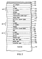
- FIG. 2 is a cross-sectional view of the solar cell of FIG. 1 after the next process step
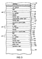
- FIG. 3 is a cross-sectional view of the solar cell of FIG. 2 after the next process step
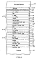
- FIG. 4 is a cross-sectional view of the solar cell of FIG. 3 after the next process step
- FIG. 5A is a cross-sectional view of the solar cell of FIG. 4 after the next process step in which the original substrate is removed;
- FIG. 5B is another cross-sectional view of the solar cell of FIG. 5A with the surrogate substrate on the bottom of the Figure;
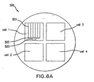
- FIG. 6A is a top plan view of a wafer in which the solar cells are fabricated
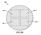
- FIG. 6B is a bottom plan view of a wafer in which the solar cells are fabricated
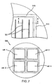
- FIG. 7 is a top plan view of the wafer of FIG. 6B after the next process step
- FIG. 8 is a cross-sectional view of the solar cell of FIG. 5A after the next process step
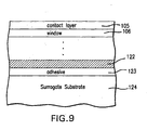
- FIG. 9 is a cross-sectional view of the solar cell of FIG. 8 after the next process step
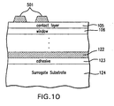
- FIG. 10 is a cross-seetional view of the solar cell of FIG. 9 after the next process step
- FIG. 11 is a cross-sectional view of the solar cell of FIG. 10 after the next process step
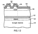
- FIG. 12 is a cross-sectional view of the solar cell of FIG. 11 after the next process step
- FIG. 13 is a cross-sectional view of the solar cell of FIG. 12 after the next process step
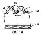
- FIG. 14 is a cross-sectional view of the solar cell of FIG. 13 after the next process step
- FIG. 15 is a cross-sectional view of the solar cell of FIG. 14 after the next process step
- FIG. 16 is an external quantum efficiency (EQE) graph of inverted metamorphic solar cell without barrier layers according to the present invention.
- FIG. 17 is an EQE graph of the middle solar subcell with and without barrier layers.
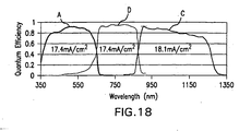
- FIG. 18 is an EQE graph of an inverted metamorphic solar cell with barrier layers according to the present invention.
- FIG. 1 depicts the multijunction solar cell according to the present invention after formation of the three subcells A, B and C on a substrate. More particularly, there is shown a substrate 101, which may be either gallium arsenide (GaAs), germanium (Ge), or other suitable material.
- a nucleation layer 102 is deposited on the substrate.
- a buffer layer 103, and an etch stop layer 104 are further deposited.
- a contact layer 105 is then deposited on layer 104, and a window layer 106 is deposited on the contact layer.
- the subcell A consisting of an n+ emitter layer 107 and a p-type base layer 108, is then deposited on the window layer 106.
- the multijunction solar cell structure could be formed by any suitable combination of group III to V elements listed in the periodic table subject to lattice constant and band gap requirements, wherein the group III includes boron (B), aluminum (Al), gallium (Ga), indium (In), and thallium (T).
- the group IV includes carbon (C), silicon (Si), germanium (Ge), and tin (Sn).
- the group V includes nitrogen (N), phosphorous (P), arsenic (As), antimony (Sb), and bismuth (Bi).
- the emitter layer 107 is composed of InQa(Al)P and the base layer is composed of InGa(Al)P.
- A1 term in parenthesis means that A1 is an optional constituent, and in this instance may be used in an amount ranging from 0% to 30%.
- BSF back surface field
- the BSF layer 109 drives minority carriers from the region near the base/BSF interface surface to minimize the effect of recombination loss.
- a BSF layer 109 reduces recombination loss at the backside of the solar subcell A and thereby reduces the recombination in the base.
- BSF layer 109 On top of the BSF layer 109 is deposited a sequence of heavily doped p-type and n-type layers 110 which forms a tunnel diode which is a circuit element to connect subcell A to subcell B.
- a window layer 111 is deposited on top of the tunnel diode layers 110 .
- the window layer 111 used in the subcell B also operates to reduce the recombination loss.
- the window layer 111 also improves the passivation of the cell surface of the underlying junctions. It should be apparent to one skilled in the art, that additional layer(s) may be added or deleted in the cell structure without departing from the scope of the present invention.
- the layers of cell B are deposited: the emitter layer 112, and the p-type base layer 113. These layers are preferably composed of InGaP and Ga(In)As respectively, although any other suitable materials consistent with lattice constant and band gap requirements may be used as well.
- a BSF layer 114 which performs the same function as the BSF layer 109.
- a p++/n++ tunnel diode 115 is deposited over the BSF layer 114 similar to the layers 110, again forming a circuit element to connect cell B to cell C.
- a barrier layer 116a preferably composed of InGa(Al)P, is deposited over the tunnel diode 115, to a thickness of about 1.0 micron.
- Such barrier layer is intended to prevent threading dislocations from propagating, either opposite to the direction of growth into the middle and top subcells B and A, or in the direction of growth into the bottom subcell C.
- the barrier layer may be any combination of III - V compound semiconductor layers having a bandgap energy greater than or equal to the grading interlayer 116, and a thickness sufficient to reduce the propagation of threading dislocations.
- Typical materials are As, P, N or Sb based III - V semiconductor materials.
- a grading interlayer or metamorphic layer 116 is deposited over the barrier layer 116a.
- Layer 116 is preferably a compositionally step-graded series of InGaAlAs layers with monotonically changing lattice constant that is intended to achieve a transition in lattice constant from subcell B to subcell C.
- the band gap of layers 116 is 1.5 eV consistent with a value slightly greater than the band gap of the middle subcell B.
- a grading interlayer may be composed of any of the As, P, N, Sb based III - V compound semiconductors subject to the constraints of having the in-plane lattice parameter greater or equal to that of the second solar cell B and less than or equal to that of the third solar cell C, and having a bandgap energy greater than that of the second solar cell B.
- the step grade contains nine compositionally graded InGaP steps with each step layer having a thickness of 0.25 micron.
- the layer 116 is composed of InGaAlAs, with monotonically changing lattice constant, over at least nine steps.
- a second barrier layer 116b is deposited over the InGaAlAs metamorphic layer 116.
- the second barrier layer 116b will have a different composition than that of barrier layer 116a, and again the base region may be GalnAs, GaAsSb, or GaInAsN.
- a window layer 117 is deposited over the barrier layer 116b, this window layer operating to reduce the recombination loss in subcell "C". It should be apparent to one skilled in the art that additional layers may be added or deleted in the cell structure without departing from the scope of the present invention.
- the layers of cell C are deposited: the n+ emitter layer 118, and the p-type base layer 119. These layers are preferably composed of InGaP and Ga(In)As respectively, although another suitable materials consistent with lattice constant and band gap requirements may be used as well.
- a BSF layer 120 is deposited on top of the cell C, the BSF layer performing the same function as the BSF layers 109 and 114.
- ap+ contact layer 121 is deposited on the BSF layer 120.
- FIG. 2 is a cross-sectional view of the solar cell of FIG. 1 after the next process step in which a metal contact layer 122 is deposited over the p+ semiconductor contact layer 121.
- the metal is preferably Ti/Au/Ag/Au.
- FIG. 3 is a cross-sectional view of the solar cell of FIG. 2 after the next process step in which an adhesive layer 123 is deposited over the metal layer 122.
- the adhesive is preferably GenTak 330 (distributed by General Chemical Corp.).
- FIG. 4 is a cross-sectional view of the solar cell of FIG. 3 after the next process step in which a surrogate substrate, preferably sapphire, is attached.
- the surrogate substrate is about 40 mils in thickness, and is perforated with holes about 1mm in diameter, spaced 4mm apart, to aid in subsequent removal of the adhesive and the substrate.
- FIG. 5A is a cross-sectional view of the solar cell of FIG. 4 after the next process step in which the original substrate is removed by a sequence of lapping and/or etching steps in which the substrate 101, the buffer layer 103, and the etch stop layer 104, are removed.
- the etchant is growth substrate dependent.
- FIG. 5B is a cross-sectional view of the solar cell of FIG. 5A from the solar cell of FIG. 5A from the orientation with the surrogate substrate 124 being at the bottom of the Figure.
- FIG. 6A is a top plan view of a wafer in which the solar cells are implemented.
- each cell there are grid lines 501 (more particularly shown in cross-section in FIG. 10 ), an interconnecting bus line 502, and a contact pad 503.
- FIG. 6B is a bottom plan view of the wafer with four solar cells shown in FIG. 6A .
- FIG. 7 is a top plan view of the wafer of FIG. 6A after the next process step in which a mesa 510 is etched around the periphery of each cell using phosphide and arsenide etchants.
- FIG. 8 is a simplified cross-sectional view of the solar cell of FIG. 5B depicting just a few of the top layers and lower layers over the surrogate substrate 124.
- FIG. 9 is a cross-sectional view of the solar cell of FIG. 8 after the next process step in which the etch stop layer 104 is removed by a HCl/H 2 O solution.
- FIG. 10 is a cross-sectional view of the solar cell of FIG. 9 after the next sequence of process steps in which a photoresist mask (not shown) is placed over the contact layer 105 to form the grid lines 501.
- the grid lines 501 are deposited via evaporation and lithographically patterned and deposited over the contact layer 105.
- the mask is lifted off to form the metal grid lines 501.
- FIG. 11 is a cross-sectional view of the solar cell of FIG. 10 after the next process step in which the grid lines are used as a mask to etch down the surface to the window layer 106 using a citric acid/peroxide etching mixture.
- FIG. 12 is a cross-sectional view of the solar cell of FIG. 11 after the next process step in which an antireflective (ARC) dielectric coating layer 130 is applied over the entire surface of the "bottom" side of the wafer with the grid lines 501.
- ARC antireflective
- FIG. 13 is a cross-sectional view of the solar cell of FIG. 12 after the next process step in which the mesa 501 is etched down to the metal layer 122 using phosphide and arsenide etchants.
- the cross-section in the figure is depicted as seen from the A-A plane shown in FIG. 7 .
- One or more silver electrodes are then welded to the contact pad(s).
- FIG. 14 is a cross-sectional view of the solar cell of FIG. 13 after the next process step after the surrogate substrate 124 and adhesive 123 are removed by EKC 922.
- the preferred perforations provided in the surrogate substrate have a diameter of 0.033 inches, and are separated by 0.152 inches.
- FIG. 15 is a cross-sectional view of the solar cell of FIG. 14 after the next process step in which an adhesive is applied over the ARC layer 130 and a coverglass attached thereto.
- FIGs. 16 through 18 Experimented indication of the efficacy of the present invention is provided in FIGs. 16 through 18 .
- External quantum efficiency (EQE) measurements were made and the results shown in FIG. 16 indicate that the long wavelength response of the middle subcell B was lower than expected.
- Nomarski microscopy indicated unexpected cross-hatching (a mode of strain relief) on the initial epitaxial layer of the lattice matched subcell A.
- Photoluminescence mapping further revealed that the luminescence of the middle subcell B was lower than expected.
- Cathodoluminescence measurements indicated that the threading dislocation density was high in the middle subcell B, but the threading dislocations did not penetrate the top subcell A. These measurements were consistent with the EQE measurements shown in FIG.
- FIG. 17 illustrates a comparison of the EQE measurements of a middle subcell in a triple junction solar cell with and without the addition of the barrier layer 116a according to the present invention.
- the graph of subcell B (without the barrier layer) has an integrated current (AMO) of 15.6 mA/cm 2 and lower EQE than that of subcell D (with the barrier layer), has an integrated current AMO) of 17.4 mA/cm 2 .
- Figure 16 is an EQE for the solar cell of FIG, 1 without a barrier layer
- Figure 18 is an EQE for the solar cell with a barrier layer.
- the current of the middle subcell B of the solar cell of Figure 18 (17.4 mA/cm 2 ) is only slightly below the current of the top subcell C (18.4 mA/cm 2 ).
- Such close current matching of the middle subcell and the top subcell demonstrates the efficacy of the present invention.
- the subcells may alternatively be contacted by means of metal contacts to laterally conductive semiconductor layers between the subcells. Such arrangements may be used to form 3-terminal, 4-terminal, and in general, n-terminal devices.
- the subcells can be interconnected in circuits using these additional terminals such that most of the available photogenerated current density in each subcell can be used effectively, leading to high efficiency for the multijunction cell, notwithstanding that the photogenerated current densities are typically different in the various subcells.
- the present invention may utilize one or more homojunction cells or subcells, i.e., a cell or subcell in which the p-n junction is formed between a p-type semiconductor and an n-type semiconductors both of which have the same chemical composition and the same band gap, differing only in the dopant species and types.
- Subcell A with p-type and n-type InGaP is one example of a homojunction subcell.
- the present invention may utilize one or more heterojunction cells or subcells, i.e., a cell or subcell in which the p-n junction is formed between a p-type semiconductor and an n-type semiconductor having different chemical compositions of the semiconductor material in the n-type and n-type regions, and/or different band gap energies in the p-type regions, in addition to utilizing different dopant species and type in the p-type and n-type regions that form the p-n junction.
- heterojunction cells or subcells i.e., a cell or subcell in which the p-n junction is formed between a p-type semiconductor and an n-type semiconductor having different chemical compositions of the semiconductor material in the n-type and n-type regions, and/or different band gap energies in the p-type regions, in addition to utilizing different dopant species and type in the p-type and n-type regions that form the p-n junction.
- the composition of the window or BSF layers may utilize other semiconductor compounds, subject to lattice constant and bandgap requirements, and may include AlInP, AlAs, AlP, AlGaInP. AlGaAsP, AlGaInAs, AlGaInPAs, OaInP, GaInAs, GaInPAs, AlGaAs, AlInAs, AlInPAs, GaAsSb, AlAsSb, GaAlAsSb, AlInSb, GaInSb, AlGaInSb, AIN, GaN, InN, GaInN, AlGaInN, GaInNAs, AlGaInNAs, ZnSSe, CdSSe, and similar materials, and still fall within the scope of the present invention.
Landscapes
- Photovoltaic Devices (AREA)
Claims (20)
- Ein Verfahren zur Ausbildung einer Multijunction-Solarzelle mit einer oberen Subzelle (C), einer mittleren Subzelle (B) und einer unteren Subzelle (A), wobei das Verfahren folgende Schritte in der folgenden Reihenfolge aufweist:Vorsehen eines ersten Substrats (101) für das Epitaxial-Wachstum des Halbleitermaterials;Ausbildung einer ersten solaren Subzelle (A) auf dem Substrat mit einem ersten Bandabstand;Ausbilden einer zweiten solaren Subzelle (B) über der ersten solaren Subzelle (A) mit einem zweiten Bandabstand, der kleiner ist als der erste Bandabstand;Ausbilden einer ersten vergrabenen Schicht (Barrier-Schicht) (116a) über der zweiten Subzelle (B);Ausbilden einer Gradier-Zwischenschicht (Schicht mit monoton sich änderndem Parameter) (116) über der vergrabenen Schicht (116a), wobei die Gradier-Zwischenschicht (116) einen dritten Bandabstand besitzt, der größer ist als der zweite Bandabstand;Ausbilden einer zweiten vergrabenen Schicht (116b) über der erwähnten Gradier-Zwischenschicht (116) und Ausbilden einer dritten solaren Subzelle (C) über der Gradier-Zwischenschicht (116) mit einem vierten Bandabstand, der kleiner ist als der zweite Bandabstand derart, dass die dritte Subzelle (C) gitterfehlangepasst bezüglich der zweiten Subzelle (B) ist, dadurch gekennzeichnet, dassdie erwähnten ersten (116a) und zweiten (116b) vergrabenen Schichten aufgebaut sind aus irgendeinem der As-, P-, N- oder Sb-basierenden III-V Verbindungshalbleiter,wobei die zweite vergrabene Schicht (116b) eine unterschiedliche Zusammensetzung gegenüber derjenigen der ersten vergrabenen Schicht (116a) besitzt; undwobei die erste vergrabene Schicht (116a) und die zweite vergrabene Schicht (116b) aufgebaut sind aus einem geeigneten Material und Gitterkonstante zur Verhinderung der Fortpflanzung von fadenförmigen bzw. Durchsetzungs-Versetzungen (threading dislocations).
- Verfahren nach Anspruch 1, wobei die erste vergrabene Schicht (116a) eine Bandabstands- bzw. Bandkantenenergie besitzt, die größer ist als oder gleich der der Gradier-Zwischenschicht.
- Verfahren nach Anspruch 1, wobei die zweite vergrabene Schicht (116b) eine Bandabstandsenergie besitzt, die größer ist als oder gleich der der ersten Gradier-Zwischenschicht (116a).
- Verfahren nach Anspruch 1, wobei das erste Substrat (101) aus der Gruppe ausgewählt ist, die aus Germanium oder GaAs besteht.
- Verfahren nach Anspruch 1, wobei die erwähnte erste solare Subzelle (A) aufgebaut ist aus einer InGa(Al)P Emitterzone (Emitterbereich) und einer InGa(Al)P-Basiszone (Basisbereich).
- Verfahren nach Anspruch 5, wobei die zweite Solarzelle (B) aufgebaut ist aus einer GaInP, GaInAs, GaAsSb oder GaInAsN Emitterzone und einer GaInAs, GaAsSb oder GaInAsN Basiszone.
- Verfahren nach Anspruch 1, wobei die Gradier-Zwischenschicht (116) aufgebaut ist aus irgendeinem der As-, P-, N-, Sb-basierenden III-V Verbindungshalbleiter und zwar unter Berücksichtigung der Einschränkungen, dass der "In-Ebene"-Gitterparameter größer ist oder gleich dem der zweiten Solarzelle (B) und kleiner als oder gleich dem der dritten Solarzelle (C) und mit einer Bandabstands- bzw. Bandkantenenergie größer als der der zweiten Solarzelle (B).
- Verfahren nach Anspruch 5, wobei die zweite solare Subzelle (B) aufgebaut ist aus einer InGaP Emitterzone und einer GaAs Basiszone.
- Verfahren nach Anspruch 1, wobei die Gradier-Zwischenschicht (116) aufgebaut ist aus InGaAIAs.
- Verfahren nach Anspruch 7, wobei die Gradier-Zwischenschicht (116) aufgebaut ist aus neun Stufen von Schichten mit sich monoton ändernder Gitterkonstanten.
- Verfahren nach Anspruch 1, wobei ferner eine Kontaktschicht (121) über der dritten solaren Subzelle (C) abgeschieden ist und elektrischen Kontakt damit vorsieht.
- Verfahren nach Anspruch 9, wobei ein zweites Surrogat-Substrat (124) über der Kontaktschicht (121) angebracht ist und das erste Substrat (101) entfernt wird.
- Verfahren nach Anspruch 1, wobei ferner Folgendes vorgesehen ist:Mustern einer Kontaktschicht (105) in ein Gitter; undÄtzen eines Trogs um den Umfand der Solarzelle herum, um so eine Mesa-Struktur auf dem zweiten Surrogat-Substrat (124) zu bilden.
- Eine Multijunction-Solarzelle, die Folgendes aufweist:ein Substrat (101);eine erste solare Subzelle (A) auf dem Substrat (101) mit einem ersten Bandabstand;eine zweite solare Subzelle (B), angeordnet über der ersten Subzelle (A) und mit einem zweiten Bandabstand, der kleiner ist als der erste Bandabstand;eine erste vergrabene Schicht (116a), angeordnet über der zweien Subzelle (B);eine Gradier-Zwischenschicht (116), angeordnet über der ersten vergrabenen Schicht (116a) und mit einem dritten Bandabstand, der größer ist als der zweite Bandabstand;eine zweite vergrabene Schicht (116b) über der Gradierschicht (116); undeine dritte solare Subzelle (C), angeordnet über der erwähnten Gradier-Zwischenschicht (116), die gitterfehlangepasst ist bezüglich der zweiten Subzelle (B) und einem vierten Bandabstand hat, der kleiner ist als der zweite Bandabstand,wobei die Solarzelle dadurch gekennzeichnet ist, dass die erste vergrabene Schicht (116a) und die zweite vergrabene Schicht (116b) aufgebaut sind aus irgendeinem der As-, P-, N- oder Sb-basierenden III-V Verbindungshalbleiter,wobei die zweite vergrabene Schicht (116b) eine unterschiedliche Zusammensetzung besitzt als die der ersten vergrabenen Schicht (116a); unddie erste vergrabene Schicht (116a) und die zweite vergrabene Schicht (116b) aufgebaut sind aus einem geeigneten Material und mit geeigneten Gitterkonstanten, um die Fortpflanzung fadenförmiger Versetzungen von (threading dislocations) zu verhindern.
- Eine Solarzelle nach Anspruch 14, wobei die vergrabene Schicht (116a) eine Bandabstands- bzw. Bandkantenenergie besitzt, die größer ist als oder gleich der der Gradier-Zwischenschicht (116).
- Eine Solarzelle nach Anspruch 14, wobei die zweite Sperrschicht (116b) eine Bandabstandsenergie besitzt, die größer ist als oder gleich der der Gradier-Zwischenschicht (116).
- Eine Solarzelle nach Anspruch 14, wobei das Substrat (101) ausgewählt ist aus der aus Germanium oder GaAs bestehenden Gruppe.
- Eine Solarzelle nach Anspruch 14, wobei die erste solare Subzelle (A) aufgebaut ist aus InGa(AI)P.
- Eine Solarzelle nach Anspruch 14, wobei die zweite solare Subzelle (B) aufgebaut ist aus einer GaInP, GaInAs, GaAsSb oder GaInAsN Emitterzone und einer GaInAs, GaAsSb oder GaInAsN Basiszone.
- Eine Solarzelle nach Anspruch 14, wobei die dritte solare Subzelle (C) aufgebaut ist aus InGaAs.
Priority Applications (2)
| Application Number | Priority Date | Filing Date | Title |
|---|---|---|---|
| AT08013467T ATE511704T1 (de) | 2008-07-25 | 2008-07-25 | Sperrschichten in umgekehrten metamorphischen multiverbindungssolarzellen |
| EP08013467A EP2148378B1 (de) | 2008-07-25 | 2008-07-25 | Sperrschichten in umgekehrten metamorphischen Multiverbindungssolarzellen |
Applications Claiming Priority (1)
| Application Number | Priority Date | Filing Date | Title |
|---|---|---|---|
| EP08013467A EP2148378B1 (de) | 2008-07-25 | 2008-07-25 | Sperrschichten in umgekehrten metamorphischen Multiverbindungssolarzellen |
Publications (2)
| Publication Number | Publication Date |
|---|---|
| EP2148378A1 EP2148378A1 (de) | 2010-01-27 |
| EP2148378B1 true EP2148378B1 (de) | 2011-06-01 |
Family
ID=40158597
Family Applications (1)
| Application Number | Title | Priority Date | Filing Date |
|---|---|---|---|
| EP08013467A Revoked EP2148378B1 (de) | 2008-07-25 | 2008-07-25 | Sperrschichten in umgekehrten metamorphischen Multiverbindungssolarzellen |
Country Status (2)
| Country | Link |
|---|---|
| EP (1) | EP2148378B1 (de) |
| AT (1) | ATE511704T1 (de) |
Families Citing this family (3)
| Publication number | Priority date | Publication date | Assignee | Title |
|---|---|---|---|---|
| EP4036992B1 (de) | 2018-01-17 | 2025-04-02 | SolAero Technologies Corp. | Solarzelle mit vierfachabzweigung und solarzellenanordnungen für raumfahrtanwendungen |
| CN113644147A (zh) * | 2021-06-25 | 2021-11-12 | 北京空间飞行器总体设计部 | 一种与火星光谱匹配的三结砷化镓太阳电池 |
| CN114335215B (zh) * | 2022-03-15 | 2022-06-14 | 南昌凯迅光电股份有限公司 | 一种带有渐变隧穿结的砷化镓太阳电池及其制作方法 |
Family Cites Families (3)
| Publication number | Priority date | Publication date | Assignee | Title |
|---|---|---|---|---|
| US6951819B2 (en) * | 2002-12-05 | 2005-10-04 | Blue Photonics, Inc. | High efficiency, monolithic multijunction solar cells containing lattice-mismatched materials and methods of forming same |
| US8536445B2 (en) * | 2006-06-02 | 2013-09-17 | Emcore Solar Power, Inc. | Inverted metamorphic multijunction solar cells |
| US20080245409A1 (en) * | 2006-12-27 | 2008-10-09 | Emcore Corporation | Inverted Metamorphic Solar Cell Mounted on Flexible Film |
-
2008
- 2008-07-25 AT AT08013467T patent/ATE511704T1/de not_active IP Right Cessation
- 2008-07-25 EP EP08013467A patent/EP2148378B1/de not_active Revoked
Also Published As
| Publication number | Publication date |
|---|---|
| ATE511704T1 (de) | 2011-06-15 |
| EP2148378A1 (de) | 2010-01-27 |
Similar Documents
| Publication | Publication Date | Title |
|---|---|---|
| CN101399298B (zh) | 倒置变质多结太阳能电池中的障壁层 | |
| US8039291B2 (en) | Demounting of inverted metamorphic multijunction solar cells | |
| CN101499495B (zh) | 倒置变形多结太阳能电池中的异质结子电池 | |
| US8236600B2 (en) | Joining method for preparing an inverted metamorphic multijunction solar cell | |
| US8969712B2 (en) | Four junction inverted metamorphic multijunction solar cell with a single metamorphic layer | |
| US9691929B2 (en) | Four junction inverted metamorphic multijunction solar cell with two metamorphic layers | |
| US20090288703A1 (en) | Wide Band Gap Window Layers In Inverted Metamorphic Multijunction Solar Cells | |
| US20090078311A1 (en) | Surfactant Assisted Growth in Barrier Layers In Inverted Metamorphic Multijunction Solar Cells | |
| US20090229658A1 (en) | Non-Isoelectronic Surfactant Assisted Growth In Inverted Metamorphic Multijunction Solar Cells | |
| US20100012174A1 (en) | High band gap contact layer in inverted metamorphic multijunction solar cells | |
| US20090272438A1 (en) | Strain Balanced Multiple Quantum Well Subcell In Inverted Metamorphic Multijunction Solar Cell | |
| US20090229662A1 (en) | Off-Cut Substrates In Inverted Metamorphic Multijunction Solar Cells | |
| US20090272430A1 (en) | Refractive Index Matching in Inverted Metamorphic Multijunction Solar Cells | |
| US20100206365A1 (en) | Inverted Metamorphic Multijunction Solar Cells on Low Density Carriers | |
| US20120211047A1 (en) | String interconnection of inverted metamorphic multijunction solar cells on flexible perforated carriers | |
| US20100229913A1 (en) | Contact Layout and String Interconnection of Inverted Metamorphic Multijunction Solar Cells | |
| US10541349B1 (en) | Methods of forming inverted multijunction solar cells with distributed Bragg reflector | |
| EP2148378B1 (de) | Sperrschichten in umgekehrten metamorphischen Multiverbindungssolarzellen | |
| US10170656B2 (en) | Inverted metamorphic multijunction solar cell with a single metamorphic layer |
Legal Events
| Date | Code | Title | Description |
|---|---|---|---|
| PUAI | Public reference made under article 153(3) epc to a published international application that has entered the european phase |
Free format text: ORIGINAL CODE: 0009012 |
|
| AK | Designated contracting states |
Kind code of ref document: A1 Designated state(s): AT BE BG CH CY CZ DE DK EE ES FI FR GB GR HR HU IE IS IT LI LT LU LV MC MT NL NO PL PT RO SE SI SK TR |
|
| AX | Request for extension of the european patent |
Extension state: AL BA MK RS |
|
| 17P | Request for examination filed |
Effective date: 20100611 |
|
| 17Q | First examination report despatched |
Effective date: 20100705 |
|
| AKX | Designation fees paid |
Designated state(s): AT BE BG CH CY CZ DE DK EE ES FI FR GB GR HR HU IE IS IT LI LT LU LV MC MT NL NO PL PT RO SE SI SK TR |
|
| GRAP | Despatch of communication of intention to grant a patent |
Free format text: ORIGINAL CODE: EPIDOSNIGR1 |
|
| GRAS | Grant fee paid |
Free format text: ORIGINAL CODE: EPIDOSNIGR3 |
|
| GRAA | (expected) grant |
Free format text: ORIGINAL CODE: 0009210 |
|
| AK | Designated contracting states |
Kind code of ref document: B1 Designated state(s): AT BE BG CH CY CZ DE DK EE ES FI FR GB GR HR HU IE IS IT LI LT LU LV MC MT NL NO PL PT RO SE SI SK TR |
|
| REG | Reference to a national code |
Ref country code: GB Ref legal event code: FG4D |
|
| REG | Reference to a national code |
Ref country code: CH Ref legal event code: EP |
|
| REG | Reference to a national code |
Ref country code: IE Ref legal event code: FG4D |
|
| REG | Reference to a national code |
Ref country code: DE Ref legal event code: R096 Ref document number: 602008007332 Country of ref document: DE Effective date: 20110714 |
|
| REG | Reference to a national code |
Ref country code: NL Ref legal event code: VDEP Effective date: 20110601 |
|
| PG25 | Lapsed in a contracting state [announced via postgrant information from national office to epo] |
Ref country code: SE Free format text: LAPSE BECAUSE OF FAILURE TO SUBMIT A TRANSLATION OF THE DESCRIPTION OR TO PAY THE FEE WITHIN THE PRESCRIBED TIME-LIMIT Effective date: 20110601 Ref country code: HR Free format text: LAPSE BECAUSE OF FAILURE TO SUBMIT A TRANSLATION OF THE DESCRIPTION OR TO PAY THE FEE WITHIN THE PRESCRIBED TIME-LIMIT Effective date: 20110601 Ref country code: NO Free format text: LAPSE BECAUSE OF FAILURE TO SUBMIT A TRANSLATION OF THE DESCRIPTION OR TO PAY THE FEE WITHIN THE PRESCRIBED TIME-LIMIT Effective date: 20110901 Ref country code: LT Free format text: LAPSE BECAUSE OF FAILURE TO SUBMIT A TRANSLATION OF THE DESCRIPTION OR TO PAY THE FEE WITHIN THE PRESCRIBED TIME-LIMIT Effective date: 20110601 |
|
| PG25 | Lapsed in a contracting state [announced via postgrant information from national office to epo] |
Ref country code: CY Free format text: LAPSE BECAUSE OF FAILURE TO SUBMIT A TRANSLATION OF THE DESCRIPTION OR TO PAY THE FEE WITHIN THE PRESCRIBED TIME-LIMIT Effective date: 20110601 Ref country code: ES Free format text: LAPSE BECAUSE OF FAILURE TO SUBMIT A TRANSLATION OF THE DESCRIPTION OR TO PAY THE FEE WITHIN THE PRESCRIBED TIME-LIMIT Effective date: 20110912 Ref country code: AT Free format text: LAPSE BECAUSE OF FAILURE TO SUBMIT A TRANSLATION OF THE DESCRIPTION OR TO PAY THE FEE WITHIN THE PRESCRIBED TIME-LIMIT Effective date: 20110601 Ref country code: LV Free format text: LAPSE BECAUSE OF FAILURE TO SUBMIT A TRANSLATION OF THE DESCRIPTION OR TO PAY THE FEE WITHIN THE PRESCRIBED TIME-LIMIT Effective date: 20110601 Ref country code: FI Free format text: LAPSE BECAUSE OF FAILURE TO SUBMIT A TRANSLATION OF THE DESCRIPTION OR TO PAY THE FEE WITHIN THE PRESCRIBED TIME-LIMIT Effective date: 20110601 Ref country code: GR Free format text: LAPSE BECAUSE OF FAILURE TO SUBMIT A TRANSLATION OF THE DESCRIPTION OR TO PAY THE FEE WITHIN THE PRESCRIBED TIME-LIMIT Effective date: 20110902 Ref country code: SI Free format text: LAPSE BECAUSE OF FAILURE TO SUBMIT A TRANSLATION OF THE DESCRIPTION OR TO PAY THE FEE WITHIN THE PRESCRIBED TIME-LIMIT Effective date: 20110601 |
|
| PG25 | Lapsed in a contracting state [announced via postgrant information from national office to epo] |
Ref country code: MT Free format text: LAPSE BECAUSE OF FAILURE TO SUBMIT A TRANSLATION OF THE DESCRIPTION OR TO PAY THE FEE WITHIN THE PRESCRIBED TIME-LIMIT Effective date: 20110601 Ref country code: BE Free format text: LAPSE BECAUSE OF FAILURE TO SUBMIT A TRANSLATION OF THE DESCRIPTION OR TO PAY THE FEE WITHIN THE PRESCRIBED TIME-LIMIT Effective date: 20110601 Ref country code: NL Free format text: LAPSE BECAUSE OF FAILURE TO SUBMIT A TRANSLATION OF THE DESCRIPTION OR TO PAY THE FEE WITHIN THE PRESCRIBED TIME-LIMIT Effective date: 20110601 |
|
| PG25 | Lapsed in a contracting state [announced via postgrant information from national office to epo] |
Ref country code: CZ Free format text: LAPSE BECAUSE OF FAILURE TO SUBMIT A TRANSLATION OF THE DESCRIPTION OR TO PAY THE FEE WITHIN THE PRESCRIBED TIME-LIMIT Effective date: 20110601 Ref country code: IS Free format text: LAPSE BECAUSE OF FAILURE TO SUBMIT A TRANSLATION OF THE DESCRIPTION OR TO PAY THE FEE WITHIN THE PRESCRIBED TIME-LIMIT Effective date: 20111001 Ref country code: EE Free format text: LAPSE BECAUSE OF FAILURE TO SUBMIT A TRANSLATION OF THE DESCRIPTION OR TO PAY THE FEE WITHIN THE PRESCRIBED TIME-LIMIT Effective date: 20110601 Ref country code: PT Free format text: LAPSE BECAUSE OF FAILURE TO SUBMIT A TRANSLATION OF THE DESCRIPTION OR TO PAY THE FEE WITHIN THE PRESCRIBED TIME-LIMIT Effective date: 20111003 |
|
| PG25 | Lapsed in a contracting state [announced via postgrant information from national office to epo] |
Ref country code: MC Free format text: LAPSE BECAUSE OF NON-PAYMENT OF DUE FEES Effective date: 20110731 Ref country code: PL Free format text: LAPSE BECAUSE OF FAILURE TO SUBMIT A TRANSLATION OF THE DESCRIPTION OR TO PAY THE FEE WITHIN THE PRESCRIBED TIME-LIMIT Effective date: 20110601 Ref country code: RO Free format text: LAPSE BECAUSE OF FAILURE TO SUBMIT A TRANSLATION OF THE DESCRIPTION OR TO PAY THE FEE WITHIN THE PRESCRIBED TIME-LIMIT Effective date: 20110601 Ref country code: SK Free format text: LAPSE BECAUSE OF FAILURE TO SUBMIT A TRANSLATION OF THE DESCRIPTION OR TO PAY THE FEE WITHIN THE PRESCRIBED TIME-LIMIT Effective date: 20110601 |
|
| PLAZ | Examination of admissibility of opposition: despatch of communication + time limit |
Free format text: ORIGINAL CODE: EPIDOSNOPE2 |
|
| PLBI | Opposition filed |
Free format text: ORIGINAL CODE: 0009260 |
|
| PLBA | Examination of admissibility of opposition: reply received |
Free format text: ORIGINAL CODE: EPIDOSNOPE4 |
|
| PLAX | Notice of opposition and request to file observation + time limit sent |
Free format text: ORIGINAL CODE: EPIDOSNOBS2 |
|
| 26 | Opposition filed |
Opponent name: AZUR SPACE SOLAR POWER GMBH Effective date: 20120301 |
|
| REG | Reference to a national code |
Ref country code: IE Ref legal event code: MM4A |
|
| REG | Reference to a national code |
Ref country code: DE Ref legal event code: R026 Ref document number: 602008007332 Country of ref document: DE Effective date: 20120301 |
|
| PG25 | Lapsed in a contracting state [announced via postgrant information from national office to epo] |
Ref country code: DK Free format text: LAPSE BECAUSE OF FAILURE TO SUBMIT A TRANSLATION OF THE DESCRIPTION OR TO PAY THE FEE WITHIN THE PRESCRIBED TIME-LIMIT Effective date: 20110601 |
|
| PG25 | Lapsed in a contracting state [announced via postgrant information from national office to epo] |
Ref country code: IE Free format text: LAPSE BECAUSE OF NON-PAYMENT OF DUE FEES Effective date: 20110725 |
|
| PLBB | Reply of patent proprietor to notice(s) of opposition received |
Free format text: ORIGINAL CODE: EPIDOSNOBS3 |
|
| REG | Reference to a national code |
Ref country code: CH Ref legal event code: PL |
|
| GBPC | Gb: european patent ceased through non-payment of renewal fee |
Effective date: 20120725 |
|
| PG25 | Lapsed in a contracting state [announced via postgrant information from national office to epo] |
Ref country code: CH Free format text: LAPSE BECAUSE OF NON-PAYMENT OF DUE FEES Effective date: 20120731 Ref country code: LI Free format text: LAPSE BECAUSE OF NON-PAYMENT OF DUE FEES Effective date: 20120731 Ref country code: GB Free format text: LAPSE BECAUSE OF NON-PAYMENT OF DUE FEES Effective date: 20120725 |
|
| PG25 | Lapsed in a contracting state [announced via postgrant information from national office to epo] |
Ref country code: LU Free format text: LAPSE BECAUSE OF NON-PAYMENT OF DUE FEES Effective date: 20110725 |
|
| PG25 | Lapsed in a contracting state [announced via postgrant information from national office to epo] |
Ref country code: BG Free format text: LAPSE BECAUSE OF FAILURE TO SUBMIT A TRANSLATION OF THE DESCRIPTION OR TO PAY THE FEE WITHIN THE PRESCRIBED TIME-LIMIT Effective date: 20110901 |
|
| PG25 | Lapsed in a contracting state [announced via postgrant information from national office to epo] |
Ref country code: TR Free format text: LAPSE BECAUSE OF FAILURE TO SUBMIT A TRANSLATION OF THE DESCRIPTION OR TO PAY THE FEE WITHIN THE PRESCRIBED TIME-LIMIT Effective date: 20110601 |
|
| PG25 | Lapsed in a contracting state [announced via postgrant information from national office to epo] |
Ref country code: HU Free format text: LAPSE BECAUSE OF FAILURE TO SUBMIT A TRANSLATION OF THE DESCRIPTION OR TO PAY THE FEE WITHIN THE PRESCRIBED TIME-LIMIT Effective date: 20110601 |
|
| APAH | Appeal reference modified |
Free format text: ORIGINAL CODE: EPIDOSCREFNO |
|
| APBM | Appeal reference recorded |
Free format text: ORIGINAL CODE: EPIDOSNREFNO |
|
| APBP | Date of receipt of notice of appeal recorded |
Free format text: ORIGINAL CODE: EPIDOSNNOA2O |
|
| APAL | Date of receipt of statement of grounds of an appeal modified |
Free format text: ORIGINAL CODE: EPIDOSCNOA3O |
|
| APBQ | Date of receipt of statement of grounds of appeal recorded |
Free format text: ORIGINAL CODE: EPIDOSNNOA3O |
|
| REG | Reference to a national code |
Ref country code: FR Ref legal event code: TP Owner name: SOLAERO TECHNOLOGIES CORP., US Effective date: 20150323 |
|
| RAP2 | Party data changed (patent owner data changed or rights of a patent transferred) |
Owner name: SOLAERO TECHNOLOGIES CORP. |
|
| REG | Reference to a national code |
Ref country code: FR Ref legal event code: PLFP Year of fee payment: 9 |
|
| REG | Reference to a national code |
Ref country code: FR Ref legal event code: PLFP Year of fee payment: 10 |
|
| REG | Reference to a national code |
Ref country code: FR Ref legal event code: PLFP Year of fee payment: 11 |
|
| PGFP | Annual fee paid to national office [announced via postgrant information from national office to epo] |
Ref country code: FR Payment date: 20180612 Year of fee payment: 11 |
|
| REG | Reference to a national code |
Ref country code: DE Ref legal event code: R064 Ref document number: 602008007332 Country of ref document: DE Ref country code: DE Ref legal event code: R103 Ref document number: 602008007332 Country of ref document: DE |
|
| APBU | Appeal procedure closed |
Free format text: ORIGINAL CODE: EPIDOSNNOA9O |
|
| RDAF | Communication despatched that patent is revoked |
Free format text: ORIGINAL CODE: EPIDOSNREV1 |
|
| STAA | Information on the status of an ep patent application or granted ep patent |
Free format text: STATUS: PATENT REVOKED |
|
| RDAG | Patent revoked |
Free format text: ORIGINAL CODE: 0009271 |
|
| PGFP | Annual fee paid to national office [announced via postgrant information from national office to epo] |
Ref country code: DE Payment date: 20180710 Year of fee payment: 11 Ref country code: IT Payment date: 20180713 Year of fee payment: 11 |
|
| 27W | Patent revoked |
Effective date: 20180906 |