EP2148455A1 - Dispositif et méthode produisant un signal optique modulé de rz-dpsk - Google Patents
Dispositif et méthode produisant un signal optique modulé de rz-dpsk Download PDFInfo
- Publication number
- EP2148455A1 EP2148455A1 EP07845730A EP07845730A EP2148455A1 EP 2148455 A1 EP2148455 A1 EP 2148455A1 EP 07845730 A EP07845730 A EP 07845730A EP 07845730 A EP07845730 A EP 07845730A EP 2148455 A1 EP2148455 A1 EP 2148455A1
- Authority
- EP
- European Patent Office
- Prior art keywords
- converter
- amplifier
- signal
- data
- modulated optical
- Prior art date
- Legal status (The legal status is an assumption and is not a legal conclusion. Google has not performed a legal analysis and makes no representation as to the accuracy of the status listed.)
- Ceased
Links
- 230000003287 optical effect Effects 0.000 title claims abstract description 89
- 238000000034 method Methods 0.000 title claims abstract description 26
- 229910003327 LiNbO3 Inorganic materials 0.000 claims abstract description 39
- 230000007274 generation of a signal involved in cell-cell signaling Effects 0.000 claims abstract description 23
- 230000001360 synchronised effect Effects 0.000 claims abstract description 17
- 238000006243 chemical reaction Methods 0.000 claims description 2
- 230000005540 biological transmission Effects 0.000 description 12
- 238000010586 diagram Methods 0.000 description 8
- 238000005516 engineering process Methods 0.000 description 6
- 230000007423 decrease Effects 0.000 description 3
- 238000011161 development Methods 0.000 description 3
- 238000004891 communication Methods 0.000 description 2
- 230000007547 defect Effects 0.000 description 2
- 239000013307 optical fiber Substances 0.000 description 2
- 230000005693 optoelectronics Effects 0.000 description 2
- 230000010363 phase shift Effects 0.000 description 2
- 238000013461 design Methods 0.000 description 1
- 239000006185 dispersion Substances 0.000 description 1
- 238000002474 experimental method Methods 0.000 description 1
- 239000000835 fiber Substances 0.000 description 1
- 230000010354 integration Effects 0.000 description 1
- 230000009022 nonlinear effect Effects 0.000 description 1
- 230000010287 polarization Effects 0.000 description 1
- 230000035945 sensitivity Effects 0.000 description 1
- 230000008054 signal transmission Effects 0.000 description 1
- 230000001629 suppression Effects 0.000 description 1
- 230000002194 synthesizing effect Effects 0.000 description 1
Images


Classifications
-
- H—ELECTRICITY
- H04—ELECTRIC COMMUNICATION TECHNIQUE
- H04B—TRANSMISSION
- H04B10/00—Transmission systems employing electromagnetic waves other than radio-waves, e.g. infrared, visible or ultraviolet light, or employing corpuscular radiation, e.g. quantum communication
- H04B10/50—Transmitters
- H04B10/516—Details of coding or modulation
- H04B10/548—Phase or frequency modulation
- H04B10/556—Digital modulation, e.g. differential phase shift keying [DPSK] or frequency shift keying [FSK]
- H04B10/5561—Digital phase modulation
-
- H—ELECTRICITY
- H04—ELECTRIC COMMUNICATION TECHNIQUE
- H04B—TRANSMISSION
- H04B10/00—Transmission systems employing electromagnetic waves other than radio-waves, e.g. infrared, visible or ultraviolet light, or employing corpuscular radiation, e.g. quantum communication
- H04B10/50—Transmitters
- H04B10/501—Structural aspects
- H04B10/503—Laser transmitters
- H04B10/505—Laser transmitters using external modulation
- H04B10/5055—Laser transmitters using external modulation using a pre-coder
-
- H—ELECTRICITY
- H04—ELECTRIC COMMUNICATION TECHNIQUE
- H04B—TRANSMISSION
- H04B10/00—Transmission systems employing electromagnetic waves other than radio-waves, e.g. infrared, visible or ultraviolet light, or employing corpuscular radiation, e.g. quantum communication
- H04B10/50—Transmitters
- H04B10/516—Details of coding or modulation
- H04B10/5162—Return-to-zero modulation schemes
Definitions
- the present invention relates to optical communication field, and especially, to a RZ-DPSK modulated optical signal generation apparatus and method.
- the modulated optical signal produced by dense wavelength division multiplexed optical transmission system with super capacity, long distance and ultra-long span requires high optical signal noise ratio (OSNR) tolerance, high ability of resisting nonlinear effects, high chromatic dispersion tolerance, and etc.
- OSNR optical signal noise ratio
- new demands directly lead to generate many new type modulation technologies, such as a return to zero (RZ) modulated optical signal, a carrier suppression return to zero (CS-RZ) modulated optical signal, a minimum shift keying (MSK) modulated optical signal, a Duobinary modulated optical signal and a return to zero differential phase shift keying (RZ-DPSK) modulated optical signal and etc.
- RZ-DPSK modulation improves the sensitivity and optical signal noise ratio performance and has good nonlinear resisting ability, thus becoming mainly selected optical modulation technology for optical transmission system with large capacity, long distance and long span transmission system, so this technology has drawn much attention from the public in recent years.
- Conventional RZ-DPSK modulated optical signal generation apparatus generally needs to be realized by a two cascade optical modulation method.
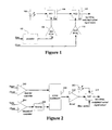
- a high speed data stream is pre-coded by a differential pre-coder 102; then the signal output by the differential pro-coder 102 is amplified by a data amplifier 104 to drive a LiNbO 3 modulator MZ1-data modulator 106, a data modulation signal with phase modulation information is obtained after a stable continuous wave laser source 108 transmitting through the LiNbO 3 modulator MZ1-data modulator 106, so as to ensure the code 0 and the code 1 in the high speed data stream have a phase difference of ⁇ .
- the NRZ code is converted into a RZ code by another LiNbO 3 modulator MZ2-clock modulator 112 drove by a clock amplifier 110.
- the obtained RZ-DPSK modulated optical signal is output at last.
- the input clock signal may be a full synchronous clock or a half synchronous clock, and the order of the two cascade modulation, namely data modulation and clock modulation, can be interchanged.
- the differential output data + and data - which have been pre-coded, with the synchronous clock respectively go through a first RZ converter 202 and a second RZ converter 204, which convert the NRZ signal into the RZ signal respectively; then, one signal going through a high speed inverter 206, together with the other converted RZ signal synthesized to be a three-level electric signal through a power synthesizer 208, and this three-level electric signal is amplified by a amplifier 210, then used to drive a LiNbO 3 modulator MZ 214, and a RZ-DPSK modulated optical signal is output from the LiNbO 3 modulator at last.
- a continuous wave laser 212 has the same function as that of the continuous wave laser 108 in figure 1 .
- this apparatus has the following defects as well: firstly, the added high speed inverter and power synthesizer, especially the use of the power synthesizer, cause the attenuation of the transmitted high speed electric signal; secondly, the two-route RZ signals go through different paths before they entering the power synthesizer, and power synthesizing the three-level signal has strict requirement to the input phase of the two RZ signals, so it is necessary to add a phase shifter in the high speed signal transmission path, which increases the complexity of the system; thirdly, the three-level signal amplifier has a high requirement and the amplitude of its output signal must reach 2V ⁇ , which still has the problems of a large power consumption and various power supply.
- a high speed data stream is converted into differential data signals after they are coded by a high speed differential pre-coder 302, then these differential data signals go through a first RZ converter 306 and a second RZ converter 308 respectively and convert the NRZ signal into a RZ signal together with the clock signal modulated by a phase shifter 304.
- a continuous wave laser 314 has the same function as that of the continuous wave laser 108 in figure 1 .
- this apparatus uses more high-speed components, such as two RZ converters, two phase-reversed RZ drivers and a high-speed phase shifter, so that the debugging complexity of the optical module is increased. Moreover, this apparatus only considers the delay relationship between the clock and the data without paying attention to the delay relationship between the two-route signals which are converted into RZ signals, which causes hidden technical defects.
- the apparatus for generating RZ-DPSK modulated optical signal in the prior art has problems in different extent, such as high price, large volume, high debugging complexity and high power consumption etc.
- the object of the present invention is to provide a practical RZ-DPSK modulated optical signal generation apparatus and method that can reduce the costs, power consumption and the volume of the optical transmission system terminal.
- a RZ-DPSK modulated optical signal generation apparatus comprises: a high speed multiplexer for amplifying high speed data signal and de-multiplexing the same into parallel low speed signals, and pre-coding the parallel low speed signals, then multiplexing the pre-coded low speed signals into a high speed pre-coding data signal, inputting a processed data + and synchronous clock into a first RZ converter and amplifier, and inputting a processed data - and synchronous clock into a second RZ converter and amplifier; the first RZ converter and amplifier and the second RZ converter and amplifier for converting NRZ signal into RZ signal and amplify them respectively, then drive the differential input LiNbO 3 modulator, the CW laser emits continuous wave optical power and transmits through the modulator, in the end output RZ-DPSK modulated optical signal.
- the RZ-DPSK modulated optical signal generation apparatus in the present invention further comprises: a phase shifter located on the data path on which the first RZ converter and amplifier locates, or located on the data path on which the second RZ converter and amplifier locates, used for ensuring the phase relationship between RZ signals.
- a RZ-DPSK modulated optical signal generation apparatus in the present invention further comprises: a continuous wave laser for providing a stable output optical power for the LiNbO 3 modulator.
- the continuous wave laser can be integrated into the LiNbO 3 modulator and it can be a broadband wavelength tunable laser.
- a RZ-DPSK modulated optical signal generation method comprises the following steps: step S502, amplify a photo-electric converted high speed data signal and de-multiplex it into parallel low speed signals through a high speed multiplexer, pre-code the parallel low speed signals, then multiplex the pre-coded low speed signals into a high speed pre-coding data signal, input processed data+ and synchronous clock into a first RZ converter and amplifier, and input processed data - and synchronous clock into a second RZ converter and amplifier; step S504, the first and second RZ converter and amplifier converts NRZ signal into a RZ signal and amplifies the RZ signal respectively, the output amplified RZ signal is used to drive a differential input modulator; and step S506, the CW laser emits continuous wave optical power and transmits through the modulator, in the end output RZ-DPSK modulated optical signal.
- a phase shifter can be located on the first RZ converter and amplifier path or on the second RZ converter and amplifier path for ensuring the phase relationship between the two RZ signals.
- the continuous wave laser provides the LiNbO 3 modulator with a stable optical power input.
- the apparatus and method proposed by the present invention can be used for generating the RZ-DPSK modulated optical signal of 10Gb/s or 40Gb/s.
- the present invention uses the LiNbO 3 modulator with differential inputs, and output signal amplitude from the driver requests the peak-to-peak value to be V ⁇ , which can reduce the power consumption greatly and need no special power supply lead to less requirement for the power supply in the transmission terminal.
- the apparatus and method according to the present invention may need no high speed phase shifter, which can decreases the debugging complexity of the optical transmission terminal and is advantageous for realization of production.
- FIG. 4 is a block diagram illustrating the RZ-DPSK modulated optical signal generation apparatus according to the embodiment of the present invention.
- the apparatus of the present invention realizes a RZ-DPSK modulated optical signal by adopting a single stage LiNbO 3 modulator.
- a high speed multiplexer 402 with pre-coder amplifies a photo-electric converted high speed data signal and demultiplexes the high speed data into 16 bit low speed signals, then multiplexes the low speed signals to a high speed pre-coded data signal, the pre-corded signal is still a NRZ format.
- a high speed data + and a data - output from the multiplexer 402 together with a synchronous clock are input into a first RZ converter and amplifier 404 and a second RZ converter and amplifier 406 respectively to convert two-route NRZ signals into RZ signals, wherein the first RZ converter and amplifier 404 and the second RZ converter and amplifier 406 are identical components.
- the two-route data signals which are converted into RZ signals are amplified and used to drive a differential input modulator 408, 410 is just a stable CW laser source, which output power transmit through the LiNbO 3 modulator 408, a RZ-DPSK modulated optical signal is output at last.
- the two-route signals which are converted into RZ signals need no phase shift; otherwise it is necessary to add a phase shifter into either the path to ensure the strict phase relationship between the two-route RZ signals.
- the two arms of the LiNbO 3 modulator 408 shall be biased previously to an appropriate bias voltage, and the continuous wave laser 410 aims to output a stable optical power to the LiNbO 3 modulator 408.
- FIG. 5 is a flow chart illustrating the RZ-DPSK modulated optical signal generation method according to the embodiment of the present invention.
- the RZ-DPSK modulated optical signal generation method of the present invention comprises the following steps: step S502, amplify a photo-electric converted high speed data signal and de-multiplex the same into parallel low speed signals by a high speed multiplexer, pre-coded the parallel low speed signals, then multiplex the pre-coded low speed signals into a high speed pre-coded data signal, input pre-coded data + and a synchronous clock into a first RZ converter and amplifier, and input pre-coded data- and synchronous clock signal into a second RZ converter and amplifier; step S504, the first RZ converter and amplifier and second RZ converter and amplifier perform RZ conversion of the input NRZ signal and amplify the converted RZ signal, then the amplified RZ signal used to drive a LiNbO 3 modulator; and step S506, a continuous wave laser emits stable optical power and transmits
- a phase shifter can be located on the first RZ converter and amplifier path or on the second RZ converter and amplifier path for ensuring the phase relationship between the two RZ signals.
- the continuous wave laser provides the LiNbO 3 modulator with a stable optical power input.
- the apparatus and method proposed by the present invention can be used to generate RZ-DPSK modulated optical signal in 10Gb/s or 40Gb/s DWDM transmission system.
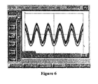
- the eye diagram of the RZ-DPSK modulated optical signal of 10Gb/s is shown in figure 6 , which is obtained by performing the following steps: emit high speed data of 9.953Gb/s and clock from the signal source to the high speed de-multiplex and multiplex with pre-coder, the multiplex component differentially outputs pre-coded data and synchronous clock into the RZ converter and amplifier, convert the NRZ signal into the RZ signal, regulate the output amplitude of the RZ signal properly to meet the requirement of the differential input LiNbO 3 modulator wherein a RZ driver outputs signals to drive the pre-biased LiNbO 3 modulator, and regulates the light source output power, we can get the optical eye diagram of RZ-DPSK modulated signal.
- the present invention is mainly used for generating the RZ-DPSK modulated optical signal of 10Gb/s and is applied to DWDM (Density Wave Division Multiplexing) transmission system
- other modulation optical signals such as the RZ-DPSK modulated optical signal of 40Gb/s
- the generation of 40Gb/s RZ-DPSK modulated optical signal according to the technical method of the present invention falls in the protection scope of the appended claims of the present application.
- the first and second RZ converter and amplifier in the above can be integrated into a single two-route NRZ to RZ converter and amplifier.
- the continuous wave laser and the LiNbO 3 modulator may be integrated into a single optoelectronic device to further decrease the volume of the whole apparatus and reduce the costs.
- the continuous wave laser may be a broadband wavelength tunable laser.
Landscapes
- Physics & Mathematics (AREA)
- Electromagnetism (AREA)
- Engineering & Computer Science (AREA)
- Computer Networks & Wireless Communication (AREA)
- Signal Processing (AREA)
- Optics & Photonics (AREA)
- Optical Communication System (AREA)
- Optical Modulation, Optical Deflection, Nonlinear Optics, Optical Demodulation, Optical Logic Elements (AREA)
Applications Claiming Priority (2)
| Application Number | Priority Date | Filing Date | Title |
|---|---|---|---|
| CNA2007100911866A CN101150370A (zh) | 2007-04-12 | 2007-04-12 | Rz-dpsk调制光信号产生装置及方法 |
| PCT/CN2007/003362 WO2008124982A1 (fr) | 2007-04-12 | 2007-11-28 | Dispositif et méthode produisant un signal optique modulé de rz-dpsk |
Publications (2)
| Publication Number | Publication Date |
|---|---|
| EP2148455A1 true EP2148455A1 (fr) | 2010-01-27 |
| EP2148455A4 EP2148455A4 (fr) | 2011-04-06 |
Family
ID=39250732
Family Applications (1)
| Application Number | Title | Priority Date | Filing Date |
|---|---|---|---|
| EP07845730A Ceased EP2148455A4 (fr) | 2007-04-12 | 2007-11-28 | Dispositif et méthode produisant un signal optique modulé de rz-dpsk |
Country Status (4)
| Country | Link |
|---|---|
| US (1) | US20100178062A1 (fr) |
| EP (1) | EP2148455A4 (fr) |
| CN (1) | CN101150370A (fr) |
| WO (1) | WO2008124982A1 (fr) |
Families Citing this family (4)
| Publication number | Priority date | Publication date | Assignee | Title |
|---|---|---|---|---|
| CN101677417A (zh) * | 2008-09-19 | 2010-03-24 | 中国科学院西安光学精密机械研究所 | 一种超高速光包交换网的光包压缩和解压缩方法及其系统 |
| CN101808063B (zh) * | 2010-03-30 | 2014-01-01 | 中兴通讯股份有限公司 | 一种控制调制器相位延迟偏置点的方法及装置 |
| CN103354210B (zh) * | 2013-06-27 | 2016-08-10 | 清华大学 | 一种键合方法及采用该键合方法形成的键合结构 |
| CN110798158B (zh) * | 2019-09-20 | 2025-02-07 | 重庆桴之科科技发展有限公司 | 一种针对车联网通信的射频功率放大器 |
Family Cites Families (14)
| Publication number | Priority date | Publication date | Assignee | Title |
|---|---|---|---|---|
| JP3027944B2 (ja) * | 1996-08-16 | 2000-04-04 | 日本電気株式会社 | 光デュオバイナリ信号光の生成方法および光送信装置 |
| JP4141028B2 (ja) * | 1998-11-25 | 2008-08-27 | 富士通株式会社 | 光デュオバイナリ伝送用の符号変換回路およびこれを用いた光送信装置および光受信装置 |
| JP4278332B2 (ja) * | 2001-06-29 | 2009-06-10 | 日本電信電話株式会社 | 光送信器および光伝送システム |
| KR100480274B1 (ko) * | 2002-11-29 | 2005-04-07 | 삼성전자주식회사 | 광위상변조기를 이용한 광전송시스템 |
| JP4554519B2 (ja) * | 2003-08-27 | 2010-09-29 | 三菱電機株式会社 | 光送信器 |
| KR100539893B1 (ko) * | 2003-11-12 | 2005-12-28 | 삼성전자주식회사 | 고밀도 파장분할다중화방식 광전송 시스템을 위한 광 송신기 |
| GB0327605D0 (en) * | 2003-11-27 | 2003-12-31 | Azea Networks Ltd | Method and apparatus for producing chirped RZ-DPSK modulated optical signals |
| KR100566196B1 (ko) * | 2003-12-01 | 2006-03-29 | 삼성전자주식회사 | 듀오바이너리 인코더 및 이를 이용한 광 듀오바이너리전송장치 |
| US7844186B2 (en) * | 2004-02-20 | 2010-11-30 | Alcatel-Lucent Usa Inc. | Method and apparatus for optical transmission |
| JP2006245647A (ja) * | 2005-02-28 | 2006-09-14 | Fujitsu Ltd | 差動位相偏移変調方式に対応した送信器及びトランスポンダ |
| JP4648093B2 (ja) * | 2005-05-31 | 2011-03-09 | 株式会社日立製作所 | 光伝送装置および集積回路装置 |
| JP4597820B2 (ja) * | 2005-09-05 | 2010-12-15 | 三菱電機株式会社 | パラレルプリコーダ回路 |
| CN1819492A (zh) * | 2006-03-16 | 2006-08-16 | 上海交通大学 | 归零-差分相移键控光调制信号的单调制器实现方法 |
| US20090047025A1 (en) * | 2007-06-04 | 2009-02-19 | Jin Hong | Multiple Electrical Level Dispersion Tolerant Optical Apparatus |
-
2007
- 2007-04-12 CN CNA2007100911866A patent/CN101150370A/zh active Pending
- 2007-11-28 EP EP07845730A patent/EP2148455A4/fr not_active Ceased
- 2007-11-28 WO PCT/CN2007/003362 patent/WO2008124982A1/fr not_active Ceased
- 2007-11-28 US US12/278,125 patent/US20100178062A1/en not_active Abandoned
Also Published As
| Publication number | Publication date |
|---|---|
| EP2148455A4 (fr) | 2011-04-06 |
| CN101150370A (zh) | 2008-03-26 |
| US20100178062A1 (en) | 2010-07-15 |
| WO2008124982A1 (fr) | 2008-10-23 |
Similar Documents
| Publication | Publication Date | Title |
|---|---|---|
| CN101896855B (zh) | 光调制器和光通信系统 | |
| US9628186B2 (en) | Advanced optical modulation generation by combining orthogonal polarized optical signals | |
| US8837947B2 (en) | Apparatus for pseudo-return-to-zero modulation | |
| US20100239264A1 (en) | Optical transmission system, apparatus and method | |
| JP5321591B2 (ja) | 光送信装置、光受信装置および光通信システム | |
| US8577224B2 (en) | Optical shaping for amplification in a semiconductor optical amplifier | |
| CN101494501B (zh) | 多码型光发射机和光信号产生的方法 | |
| JP3984220B2 (ja) | デュオバイナリ光伝送装置 | |
| EP2148455A1 (fr) | Dispositif et méthode produisant un signal optique modulé de rz-dpsk | |
| JP4053473B2 (ja) | 光送信器 | |
| US20040076439A1 (en) | Optical transmission system | |
| US8761612B2 (en) | 16 quadrature amplitude modulation optical signal transmitter | |
| KR20040106976A (ko) | 편광 듀오바이너리 광전송장치 | |
| Wei et al. | 40 Gb/s duobinary and modified duobinary transmitter based on an optical delay interferometer | |
| CN101141199B (zh) | 一种光发送系统及其方法 | |
| CN101494502B (zh) | 一种归零交替传号反转光调制信号的产生方法和装置 | |
| CN101159496B (zh) | 一种产生归零光双二进制调制信号的装置 | |
| CN101145850B (zh) | 归零交替传号反转光发射机及光信号产生方法 | |
| JP5374709B2 (ja) | 光送信器 | |
| US20070280701A1 (en) | Method and Apparatus for Producing High Extinction Ratio Data Modulation Formats | |
| US20050201760A1 (en) | Method and system for generating CS-RZ pulses showing narrow width of bit duration | |
| JP4028463B2 (ja) | 光送信装置および光送受信装置 | |
| KR101282414B1 (ko) | Rz-dpsk 및 rz-dqpsk 광 송신 장치 | |
| JP2004096653A (ja) | 光送信器及びそれに用いる光変調方法 | |
| GB2414563A (en) | Method and apparatus for producing high extinction ratio data modulation format |
Legal Events
| Date | Code | Title | Description |
|---|---|---|---|
| PUAI | Public reference made under article 153(3) epc to a published international application that has entered the european phase |
Free format text: ORIGINAL CODE: 0009012 |
|
| 17P | Request for examination filed |
Effective date: 20091112 |
|
| AK | Designated contracting states |
Kind code of ref document: A1 Designated state(s): AT BE BG CH CY CZ DE DK EE ES FI FR GB GR HU IE IS IT LI LT LU LV MC MT NL PL PT RO SE SI SK TR |
|
| AX | Request for extension of the european patent |
Extension state: AL BA HR MK RS |
|
| DAX | Request for extension of the european patent (deleted) | ||
| A4 | Supplementary search report drawn up and despatched |
Effective date: 20110303 |
|
| 17Q | First examination report despatched |
Effective date: 20160317 |
|
| REG | Reference to a national code |
Ref country code: DE Ref legal event code: R003 |
|
| STAA | Information on the status of an ep patent application or granted ep patent |
Free format text: STATUS: THE APPLICATION HAS BEEN REFUSED |
|
| 18R | Application refused |
Effective date: 20170403 |