EP2148523A2 - Optisches Zugriffssystem, optische Schalteinheit und optisches Leitungsendgerät - Google Patents
Optisches Zugriffssystem, optische Schalteinheit und optisches Leitungsendgerät Download PDFInfo
- Publication number
- EP2148523A2 EP2148523A2 EP09165967A EP09165967A EP2148523A2 EP 2148523 A2 EP2148523 A2 EP 2148523A2 EP 09165967 A EP09165967 A EP 09165967A EP 09165967 A EP09165967 A EP 09165967A EP 2148523 A2 EP2148523 A2 EP 2148523A2
- Authority
- EP
- European Patent Office
- Prior art keywords
- optical
- frame
- switch
- line terminal
- time period
- Prior art date
- Legal status (The legal status is an assumption and is not a legal conclusion. Google has not performed a legal analysis and makes no representation as to the accuracy of the status listed.)
- Withdrawn
Links
- 230000003287 optical effect Effects 0.000 title claims abstract description 347
- 238000004891 communication Methods 0.000 claims abstract description 59
- 230000005540 biological transmission Effects 0.000 claims description 39
- 238000000034 method Methods 0.000 claims description 23
- 238000012545 processing Methods 0.000 description 76
- 238000011144 upstream manufacturing Methods 0.000 description 56
- 238000010586 diagram Methods 0.000 description 33
- 239000013307 optical fiber Substances 0.000 description 8
- 238000006243 chemical reaction Methods 0.000 description 3
- 238000005516 engineering process Methods 0.000 description 3
- 239000000284 extract Substances 0.000 description 3
- 230000008054 signal transmission Effects 0.000 description 3
- 101150116046 PCBD1 gene Proteins 0.000 description 2
- 101150047335 pcbd gene Proteins 0.000 description 2
- 238000009825 accumulation Methods 0.000 description 1
- 125000004122 cyclic group Chemical group 0.000 description 1
- 238000013507 mapping Methods 0.000 description 1
- 238000012986 modification Methods 0.000 description 1
- 230000004048 modification Effects 0.000 description 1
- 230000001360 synchronised effect Effects 0.000 description 1
Images




Classifications
-
- H—ELECTRICITY
- H04—ELECTRIC COMMUNICATION TECHNIQUE
- H04Q—SELECTING
- H04Q11/00—Selecting arrangements for multiplex systems
- H04Q11/0001—Selecting arrangements for multiplex systems using optical switching
- H04Q11/0062—Network aspects
- H04Q11/0067—Provisions for optical access or distribution networks, e.g. Gigabit Ethernet Passive Optical Network (GE-PON), ATM-based Passive Optical Network (A-PON), PON-Ring
-
- H—ELECTRICITY
- H04—ELECTRIC COMMUNICATION TECHNIQUE
- H04Q—SELECTING
- H04Q11/00—Selecting arrangements for multiplex systems
- H04Q11/0001—Selecting arrangements for multiplex systems using optical switching
- H04Q11/0005—Switch and router aspects
- H04Q2011/0037—Operation
- H04Q2011/0045—Synchronisation
-
- H—ELECTRICITY
- H04—ELECTRIC COMMUNICATION TECHNIQUE
- H04Q—SELECTING
- H04Q11/00—Selecting arrangements for multiplex systems
- H04Q11/0001—Selecting arrangements for multiplex systems using optical switching
- H04Q11/0062—Network aspects
- H04Q2011/0064—Arbitration, scheduling or medium access control aspects
Definitions
- This invention relates to an optical access system, and more particularly, to a technology of controlling optical communication path switching in an optical access system that uses an optical switch to switch optical communication paths.
- PON passive optical network
- EON Ethernet passive optical network
- GPON Gigabit-capable passive optical network
- a PON includes an optical line terminal (OLT), which terminates an optical fiber on the side of a central office of a telecommunications carrier, an optical network unit (ONU), which terminates an optical fiber on the user terminal side, and a splitter, which splits an optical fiber led out of the OLT up among a plurality of the ONUs.
- OLT optical line terminal
- ONU optical network unit
- splitter which splits an optical fiber led out of the OLT up among a plurality of the ONUs.
- the splitter keeps the cost of building the network low.
- the splitter splits a signal into as many copies as the total count of ONUs, allowing the signal to reach other ONUs in addition to the originally intended receiver of the communication.
- the resultant problem is that satisfactory secrecy is not always guaranteed.
- signal branching in the splitter lowers the optical signal power and presents a problem that an increase in number of branches shortens the communicable distance.
- a unit that makes a switch to an output port for a desired ONU splits an optical signal sent from the OLT into a signal for the optical switch and a signal for a circuit that performs frame reading processing.
- a logical link identifier (LLID) set in the preamble part of an EPON frame is used in switching output ports of the optical switch.
- a delay circuit needs to be provided downstream of the optical switch in order to delay signal transmission by the amount of time required for processing in the frame reading circuit.
- the optical fiber measures 42.4 m in length and hinders the downsizing of the output port switching unit.
- an optical access system including: an optical line terminal which is connected to another network; a plurality of optical network units which are each connected to a user terminal; and/or an optical switching unit which is implemented between the optical line terminal and the plurality of optical network units to switch optical communication paths between the optical line terminal and the plurality of optical network units.
- the optical line terminal sends to the optical switching unit a control frame including a switching time when the optical switching unit is to make a switch from one of the optical communication paths between the optical line terminal and the plurality of optical network units to another, and an identifier of an optical communication path to which the switch is made in order to switch the optical communication paths between the optical line terminal and the plurality of optical network units.
- the optical switching unit switches the optical communication paths between the optical line terminal and the plurality of optical network units based on the switching time and the identifier of the optical communication path after switching which are included in the control frame.
- the optical line terminal determines a switching control schedule of an optical switch and data frame transmission timing, and conveys the determined switching control schedule and transmission timing to the optical switching unit (OSW), thereby eliminating the need for delay control of an optical signal in the OSW.
- the OSW can thus be made small in size.
- FIG. 1 is a block diagram illustrating a configuration example of a network according to a first embodiment of this invention.
- An optical access system 50 of the first embodiment includes an optical line terminal (OLT) 1, an optical switching unit (OSW) 2, and optical network units (ONUs) 3.
- the optical access system 50 includes as many ONUs 3 as the count of users.
- the ONUs 3 are referred to as ONUs 3 when there is no need to discriminate one from another, and referred to as ONUs 3-1 to 3-n when discriminating one from another is necessary.
- a plurality of user terminals 4 (4-1 to 4-n) are connected to the ONUs 3.
- the user terminals 4 communicate with a core network 55 via the optical access system 50 and a gateway (GW) 53.
- GW gateway
- FIG. 2 is a block diagram illustrating a configuration example of the OLT 1 according to the first embodiment of this invention.
- the OLT 1 includes a multiplexing/demultiplexing module (WDM) 101, an electrical-optical signal converter (E/0 converter) 102, an optical-electrical signal converter (0/E converter) 103, a frame transmission control module 104, a downstream frame processing module 105, an optical switch controller 106, a protocol control module 108, an upstream frame processing module 109, and a gateway interface (GW IF) 110.
- WDM multiplexing/demultiplexing module
- E/0 converter electrical-optical signal converter
- optical-electrical signal converter (0/E converter)
- a frame transmission control module 104 a downstream frame processing module 105
- an optical switch controller 106 a protocol control module 108
- GW IF gateway interface
- the multiplexing/demultiplexing module (WDM) 101 separates and combines an upstream optical signal (optical signal traveling from the OSW 2 to the OLT 1) and a downstream optical signal (optical signal traveling from the OLT 1 to the OSW 2) which undergo wavelength multiplexing between the OLT 1 and the OSW 2.
- the electrical-optical signal converter (E/0 converter) 102 converts an electrical signal into an optical signal.
- the optical-electrical signal converter (0/E converter) 103 converts an optical signal into an electrical signal.
- the frame transmission control module 104 controls the transmission of a frame sent to the OSW 2.
- the downstream frame processing module 105 generates a frame to be sent to the OSW 2.
- the optical switch controller 106 performs processing for controlling the OSW 2.
- the protocol control module 108 performs protocol processing for controlling communication between the OLT 1 and the ONUs 3 (specifically, processing equivalent to Multipoint Control Protocol (MPCP), which is defined in IEEE Std 802. 3TM-2005).
- MPCP Multipoint Control Protocol
- the upstream frame processing module 109 processes a frame received from the OSW 2.
- the gateway interface (GW IF) 110 is a physical line interface for the GW 53.
- the GW IF 110 of the OLT 1 receives a frame from the GW 53 and sends the received frame to the downstream frame processing module 105.
- the downstream frame processing module 105 keeps a table illustrated in FIG. 15 .
- the association between a MAC address and a logical link identifier (LLID) for identifying each ONU 3 is set in this table.
- the downstream frame processing module 105 refers to the table of FIG. 15 and, based on a destination MAC address that is attached to the received frame, obtains an LLID to be attached to a frame that is sent to the OSW 2.
- the optical switch controller 106 obtains, from the downstream frame processing module 105, information about a frame that the OLT 1 sends to the OSW 2, and obtains, from the protocol control module 108, information about time points at which the ONUs 3 send frames to the OSW 2, to thereby determine a switching schedule of an optical switch element in the OSW 2.
- the optical switch controller 106 also generates an optical switch control frame in order to notify the OSW 2 of the switching schedule of the optical switch element in the OSW 2.
- FIG. 3 is a block diagram illustrating a configuration example of the frame transmission control module 104 of the OLT 1 according to the first embodiment of this invention.
- the frame transmission control module 104 includes a data frame queue (Q_data) 1041, a selector (SEL) 1044, a downstream switch control frame queue (Q_down) 1042, an upstream switch control frame queue (Q_up) 1043, and a reading control module 1045.
- Q_data data frame queue
- SEL selector
- Q_down downstream switch control frame queue
- Q_up upstream switch control frame queue
- the data frame queue (Q_data) 1041 is a transmission queue of transmission frames generated by the downstream frame processing module 105.
- the selector (SEL) 1044 identifies whether a frame generated by the optical switch controller 106 is a downstream switch control frame or an upstream switch control frame.
- the downstream switch control frame queue (Q_down) 1042 is a transmission queue of downstream switch control frames.
- the upstream switch control frame queue (Q_up) 1043 is a transmission queue of upstream switch control frames.
- the reading control module 1045 controls the reading of data out of the queues Q_data 1041, Q_down 1042, and Q_up 1043.
- the reading control module 1045 is connected to the optical switch controller 106.
- the optical switch controller 106 notifies the reading control module 1045 of information about an optical switch control frame generated by the optical switch controller 106 in order to control the reading of transmission frames from the data frame queue 1041, the downstream switch control frame queue 1042, and the upstream switch control frame queue 1043.
- FIG. 4 is a block diagram illustrating a configuration example of the OSW 2 according to the first embodiment of this invention.
- the OSW 2 includes multiplexing/demultiplexing modules (WDM) 210-1 to 210-n, a downstream switch element 211, an upstream switch element 212, a downstream switch driver 213, an upstream switch driver 214, a downstream switch controller 215, an upstream switch controller 216, a frame processing module 217, an optical-electrical signal converter (0/E converter) 218, an electrical-optical signal converter (E/0 converter) 219, a downstream splitter 220, an upstream splitter 221, and a multiplexing/demultiplexing module (WDM) 223.
- WDM multiplexing/demultiplexing modules
- the multiplexing/demultiplexing modules (WDM) 210-1 to 210-n separate and combine an upstream optical signal and a downstream optical signal which undergo wavelength multiplexing between the OSW 2 and the ONUs 3-1 to 3-n, respectively.
- the downstream switch element 211 switches communication paths of a signal transmitted from the OSW 2 to the ONUs 3-1 to 3-n.
- the upstream switch element 212 switches communication paths of an upstream signal transmitted from the ONUs 3-1 to 3-n to the OSW 2.
- the downstream switch driver 213 is a circuit that drives the downstream switch element 211.
- the upstream switch driver 214 is a circuit that drives the upstream switch element 212.
- the downstream switch controller 215 controls a switch made by the downstream switch element 211.
- the upstream switch controller 216 controls a switch made by the upstream switch element 212.
- the frame processing module 217 processes a switch control frame received from the OLT 1.
- the optical-electrical signal converter (0/E converter) 218 converts an optical signal into an electrical signal.
- the electrical-optical signal converter (E/0 converter) 219 converts an electrical signal into an optical signal.
- the downstream splitter 220 splits an optical fiber used for downstream optical signal transmission.
- the upstream splitter 221 splits an optical fiber used for upstream optical signal transmission.
- the wavelength division multiplexer/de-multiplexer (WDM) 223 separates and combines an upstream optical signal and a downstream optical signal which undergo wavelength multiplexing between the OSW 2 and the OLT 1.
- FIGS. 16A and 16B Configurations of the switch elements 211 and 212 are illustrated in FIGS. 16A and 16B .
- the downstream switch element 211 includes one input port 2111 and n output ports 2112-1 to 2112-n. Receiving a drive signal from the switch driver 213, the downstream switch element 211 switches communication paths of a downstream signal by opening up a path between the input port 2111 and an arbitrary one of the output ports 2112-1 to 2112-n.
- the upstream switch element 212 includes one output port 2121 and n input ports 2122-1 to 2122-n. Receiving a drive signal from the switch driver 214, the upstream switch element 212 switches communication paths of an upstream signal by opening up a path between an arbitrary one of the input ports 2122-1 to 2112-n and the output port 2121.
- the WDM 223 extracts only optical signals that have a wavelength of the downstream direction from among optical signals that the OSW 2 has received from the OLT 1, and sends the extracted signals to the splitter 220.
- the splitter 220 splits each of the extracted signals into a signal for the downstream switch element 211 and a signal for the O/E converter 218.
- the downstream switch element 211 outputs the input optical signal from an output port that is open for communication with the input port.
- the optical signal output from the output port is sent to the relevant ONU 3 via the WDM 210.
- the optical signal input to the O/E converter 218 as a result of split in the splitter 220 is converted into an electrical signal.
- the electrical signal created by the conversion is input to the frame processing module 217.
- the frame processing module 217 extracts a frame from the input electrical signal, and performs frame processing illustrated in FIG. 14 .
- FIG. 17 is a diagram illustrating a configuration example of a table in which the association relation between an input/output port number of an optical switch element and an LLID is set according to the first embodiment of this invention.
- This table includes an input/output port number of an optical switch element and an LLID assigned to the ONU 3 that is connected to the input/output port.
- the table is provided in the downstream switch controller 215 or upstream switch controller 216 of the OSW 2.
- the OSW 2 receives an optical switch control frame illustrated in FIG. 10 and extracts an LLID value from the optical switch control frame.
- the OSW 2 refers to the table illustrated in FIG. 17 to convert the extracted LLID value into an input/output port number.
- the input/output port number obtained by the conversion is used by the downstream switch controller 215 in determining to which port the downstream switch element 211 should switch, and by the upstream switch controller 216 in determining to which port the upstream switch element 212 should switch.
- the OSW 2 that has a table setting the association relation between an input/output port number of a switch element and an LLID assigned to the ONU 3 that is connected to the input/output port.
- the table can be provided in the OLT 1 instead, without causing any obstruction to the switch control of an optical switch element that is described in this embodiment.
- FIG. 5 is a diagram illustrating an example of a sequence in which the OLT 1 controls the downstream switch element 211 of the OSW 2 according to the first embodiment of this invention.
- a single optical switch control frame is used to control the downstream switch element 211 so that appropriate switches are made for the destinations of subsequent three data frames.
- the OLT 1 sends to the OSW 2 an optical switch control frame FR-C1 in which a switching schedule of the downstream switch element 211 reflecting the destinations of the three frames is set.
- the switching schedule of the downstream switch element 211 of the OSW 2 that the OLT 1 sets in the optical switch control frame FR-C1 includes the following three switches:
- the OSW 2 spends a time period Tc to process the optical switch control frame FR-C1.
- the time period Tc is a fixed value in the case where the processing is executed by a logic circuit such as an LSI.
- the OSW 2 starts output port switching processing of the downstream switch element 211 and completes the output port switching processing after a time period Ts elapses.
- the OLT 1 After a time period Ta (length of time that is the sum of the optical switch control frame processing time Tc and the output port switching processing time Ts of the downstream switch element 211 in the OSW 2) elapses since the transmission of the optical switch control frame FR-C1, the OLT 1 sends a data frame FR-D1, which is destined for the ONU 3 #1.
- the data frame FR-D1 passes through the downstream switch element 211 in which a path between the input port and an output port that is connected to the ONU 3 #1 is open.
- the optical switch control frame processing time Tc and the output port switching processing time Ts of the downstream switch element 211 in the OSW 2 are desirably set in the OLT 1 in advance.
- the OLT 1 can calculate, from the frame length of the data frame FR-D1, a length of time (Tf1) for which the data frame FR-D1, which is sent to the ONU 3 #1 by the OLT 1, takes to pass through the downstream switch element 211.
- the time point t2 at which the OSW 2 causes the downstream switch element 211 to make a switch to an output port that is connected to the ONU 3 #5 can be expressed as t1+Ts+Tf1.
- the OLT 1 starts the transmission of a data frame FR-D2, which is destined for the ONU 3 #5.
- the data frame FR-D2 sent by the OLT 1 passes through the downstream switch element 211 in which a path between the input port and an output port that is connected to the ONU 3 #5 is open at a time point t2+Ts at which output port switching processing of the downstream switch element 211 is completed.
- the OSW 2 starts output port switching processing of the downstream switch element 211 at the time point t3 (t2+Ts+Tf2).
- the OLT 1 starts the transmission of a data frame FR-D3, which is destined for the ONU 3 #3.
- the data frame FR-D3 passes through the downstream switch element 211 in which a path between the input port and an output port that is connected to the ONU 3 #3 is open.
- FIG. 6 is a diagram illustrating another example of the sequence in which the OLT 1 controls the downstream switch element 211 of the OSW 2 according to the first embodiment of this invention.
- FIG. 5 uses a single optical switch control frame to control the switching timing of an optical switch element for a plurality of subsequent data frames.
- a single control frame is used to control the switching timing of an optical switch element for a single subsequent data frame.
- the OLT 1 uses an optical switch control frame FR-C3 to instruct the OSW 2 to switch to an output port that is connected to the ONU 3 #1.
- the OSW 2 receives the optical switch control frame FR-C3 and, at a time point t4 which arrives after the time period Tc elapses since the reception of the optical switch control frame FR-C3, the OSW 2 starts output port switching processing of the downstream switch element 211.
- the OLT 1 After the time period Ta (length of time that is the sum of the optical switch control frame processing time Tc and the output port switching processing time Ts of the downstream switch element 211 in the OSW 2) elapses since the transmission of the optical switch control frame FR-C3, the OLT 1 sends a data frame FR-D4, which is destined for the ONU 3 #1.
- the data frame FR-D4 passes through the downstream switch element 211 in which a path between the input port and an output port that is connected to the ONU 3 #1 is open.
- the OLT 1 then uses an optical switch control frame FR-C4 to instruct the OSW 2 to switch to an output port that is connected to the ONU 3 #5.
- the OSW 2 receives the optical switch control frame FR-C4 and, at a time point t5 which arrives after the time period Tc elapses since the reception of the optical switch control frame FR-C4, the OSW 2 starts output port switching processing of the downstream switch element 211.
- the OLT 1 After the time period Ta (length of time that is the sum of the optical switch control frame processing time Tc and the output port switching processing time Ts of the downstream switch element 211 in the OSW 2) elapses since the transmission of the optical switch control frame FR-C4, the OLT 1 sends a data frame FR-D5, which is destined for the ONU 3 #5.
- the data frame FR-D5 passes through the downstream switch element 211 in which a path between the input port and an output port that is connected to the ONU 3 #5 is open.
- information set in the optical switch control frame needs to contain only an output port that is connected to the ONU 3 for which the subsequent data frame is destined, and the OLT 1 does not need to notify the OSW 2 of when to switch output ports of the optical switch.
- FIG. 7 is a diagram illustrating an example of a sequence in which the OLT 1 controls the upstream switch element 212 of the OSW 2 according to the first embodiment of this invention.
- the OLT 1 sends an optical switch control frame FR-C5 to the OSW 2 in order to notify the OSW 2 of a switching schedule of the downstream switch element 211.
- the OLT 1 next sends, to the ONU 3 #1, the ONU 3 #5, and the ONU 3 #3, Gate messages FR-G1, FR-G2, and FR-G3, respectively, which notify time points when the ONUs 3 are allowed to transmit their respective frames to the OLT 1.
- the Gate messages are in conformity with a Gate message of MPCP defined in IEEE Std 802. 3TM-2005.
- the OLT 1 sends an optical switch control frame FR-C6 to the OSW 2 in order to control the switching of the upstream switch element 212.
- the OLT 1 sets in the optical switch control frame FR-C6 a switching schedule of the upstream switch element 212 of the OSW 2.
- the switching schedule includes the following three switches:
- the time point t6 is expressed as t11+Tr_1 ⁇ - s by taking into account a frame transmission time point t11, which is when the ONU 3 #1 is allowed to transmit a frame by permission given from the OLT 1 through the Gate message FR-G1, a propagation delay time Tr_1 of an optical signal traveling from the ONU 3 #1 to the OSW 2, and the time period Ts required for optical switching processing.
- the time point t7 is expressed as t51+Tr_5 ⁇ - s by taking into account a frame transmission time point t51, which is when the ONU 3 #5 is allowed to transmit a frame by permission given from the OLT 1 through the Gate message FR-G2, a propagation delay time Tr_5 of an optical signal traveling from the ONU 3 #5 to the OSW 2, and the time period Ts required for optical switching processing.
- the time point t8 is expressed as t31+Tr_3 ⁇ - s by taking into account a frame transmission time point t31, which is when the ONU 3 #3 is allowed to transmit a frame by permission given from the OLT 1 through the Gate message FR-G3, a propagation delay time Tr_3 of an optical signal traveling from the ONU 3 #3 to the OSW 2, and the time period Ts required for optical switching processing.
- the ONU 3 #1, the ONU 3 #5, and the ONU 3 #3 respectively send data frames FR-D6, FR-D7, and FR-D8 to the OLT 1 in accordance with the schedule notified through the Gate messages FR-G1, FR-G2, and FR-G3.
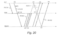
- FIG. 20 is an explanatory diagram of an example of how an optical signal propagation delay time is measured for each of the ONUs 3-1 to 3-n about an optical signal traveling from the ONU 3 to the OSW 2 according to the first embodiment of this invention.
- the OLT 1 sends a switch control frame FR-C10 to the OSW 2.
- the OSW 2 receives the switch control frame FR-C10, the OSW 2 causes the downstream switch element 211 to make a switch to one of its output ports.
- the OLT 1 sends a Gate message FR-G10, which is for discovering the connected ONU 3 #10, to the OSW 2 at a time point t10.
- a time stamp t10 is set in the Gate message FR-G10.
- the OSW 2 monitors the Gate message FR-G10 and sets the time stamp t10, which is set in the Gate message FR-G10, to a local counter.
- the Gate message FR-G10 passes through an output port of the downstream switch element 211 to which a switch has been made when instructed by the switch control frame FR-C10, and then arrives at the ONU 3 #10.
- the ONU 3 #10 receives the Gate message FR-G10 and sets the time stamp t10 in a local stamp.
- the ONU 3 #10 Once receiving the Gate message FR-G10, the ONU 3 #10 repeatedly sends a Register_Request message FR-R10 until a time point t11 (from FR-R10 to FR-R12).
- the OSW 2 causes the upstream switch element 212 to make a switch to one of its input ports that is connected to the ONU 3 #10.
- FR-R11 is the first message to arrive at the OLT 1
- a time point at which the OLT 1 receives FR-R11 is a time point t12.
- the Register_Request message FR-R12 which is sent by the ONU 3 #10 at the time point t11, passes through the OSW 2 and arrives at the OLT 1 at a time point t14.
- a half the difference between t14 and t12 is the optical signal propagation delay time between the ONU 3 #10 and the OSW 2.
- FIG. 11 is a flow chart illustrating an example of a processing procedure that is executed by the downstream frame processing module 105 of the OLT 1 according to the first embodiment of this invention.
- the downstream frame processing module 105 of the OLT 1 receives a downstream data frame (FL110) and calculates the frame length of the received data frame (FL120).
- the frame processing module 105 next searches the MAC address-LLID association table of FIG. 15 to obtain an LLID value that is associated with a destination MAC address attached to the received data frame (FL130).
- the frame processing module 105 notifies the optical switch controller 106 of the frame length obtained in Step FL120 and the LLID value obtained in Step FL130 (FL140).
- the frame processing module 105 then inputs the received data frame in the frame transmission control module 104 (FL150) and ends downstream frame processing.
- FIG. 18 is a flow chart illustrating an example of the data frame transmission procedure that is executed by the reading control module 1045 of the OLT 1 according to the first embodiment of this invention.
- the reading control module 1045 sets a value N , which is the count of data frames following a single optical switch control frame, and the value of a counter " i ", which represents the count of actually transmitted data frames, to "1" (FL505).
- the value N of the data frame count is notified from the optical switch controller 106.
- An optical switch control frame for controlling the downstream switch element 211 is then read from the downstream switch control frame queue 1042 and, after the read optical switch control frame is transmitted (FL510), a timer TM1 is activated (FL515).
- Ta is the sum of the time period Tc which the OSW 2 requires to process an optical switch control frame and the time period Ts which the OSW 2 requires to complete the switching processing of the downstream switch element 211) (FL520)
- Ta is the sum of the time period Tc which the OSW 2 requires to process an optical switch control frame and the time period Ts which the OSW 2 requires to complete the switching processing of the downstream switch element 211) (FL520)
- one data frame is taken out of the data frame queue (Q_data) 1041.
- the taken-out data frame is transmitted (FL525).
- the value of the counter " i " and the transmission frame count N are compared at this point (FL530).
- the reading control module 1045 returns to Step FL525 to take one data frame out of the data frame queue (Q_data) 1041 and to transmit the taken-out data frame.
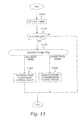
- FIG. 12 is a flow chart illustrating an example of a processing procedure relevant to downstream communication control which is executed by the optical switch controller 106 of the OLT 1 according to the first embodiment of this invention.
- the optical switch controller 106 of the OLT 1 which is illustrated in FIG. 2 performs initialization (FL200), then sets the value of the frame counter " i " to "0" (FL205), and shifts to a waiting state (FL210).
- the optical switch controller 106 calculates a switching time of the downstream switch element 211 from the notified frame length of the transmission frame so that a switch is made at the time when the frame passes through the OSW 2 (FL215).
- the optical switch controller 106 increments the value of the frame counter " i " (FL220) and identifies the counter value (FL225).
- the value of the frame counter " i " matches a threshold " m ", which is determined in advance, data frames to be controlled have been accumulated to a given maximum count, and the optical switch controller 106 therefore moves to Step FL240.
- the threshold " m " is the maximum count of downstream data frames that follow a single switch control frame.
- Step FL225 When the value of the frame counter " i " is "1" in Step FL225, the optical switch controller 106 activates a timer (FL230) and shifts to a waiting state (FL210).
- the optical switch controller 106 determines whether or not the timer has finished counting (FL235). In the case where the timer has finished counting, the optical switch controller 106 moves to Step FL240. In the case where the timer has not finished counting, the optical switch controller 106 again shifts to a waiting state (FL210).
- a switch control frame is generated in Step FL240. Thereafter, the optical switch controller 106 resets the timer (FL245) and then moves to Step FL205, where the optical switch controller 106 sets the value of the frame counter " i " to "0" in order to generate the next switch control frame, and shifts to the waiting state FL210.
- Step FL230 When the timer activated in Step FL230 finishes counting while the optical switch controller 106 is in the waiting state FL210, the optical switch controller 106 moves to Step FL240 to generate a switch control frame as in the case of moving from Steps FL225, FL230, and FL235 described above.
- This embodiment uses a maximum data frame count and a timer in controlling the generation of a switch control frame as a result of taking into consideration the fact that heavy traffic equals increased delay when the count of downstream data frames following a single switch control frame exceeds a maximum count m whereas, when data frame accumulation continues after the timer finishes counting up to a given time, light traffic equals increased delay.
- the generation of a switch control frame may be controlled with one of the maximum data frame count and the timer.
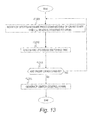
- FIG. 13 is a flow chart illustrating an example of a processing procedure relevant to upstream communication control which is executed by the optical switch controller 106 of the OLT 1 according to the first embodiment of this invention.
- the optical switch controller 106 is notified by the protocol processing module 108 of a Grant start time t_x, which is set in a Gate message destined for the ONU 3 #x (FL305). The optical switch controller 106 then calculates an upstream switching time (FL310). The upstream switching time is calculated by the method described with reference to FIG. 7 .
- the optical switch controller 106 determines whether or not there are Gate messages for other ONUs 3 (FL315). In the case where Gate messages for other ONUs 3 are found, the optical switch controller 106 returns to Step FL305. In the case where no Gage messages for other ONUs 3 are found, the optical switch controller 106 generates an upstream optical switch control frame (FL320) and ends the processing.
- FIG. 14 is a flow chart illustrating an example of a processing procedure that is executed by the frame processing module 217 of the OSW 2 according to the first embodiment of this invention.
- the splitter 220 splits an optical signal received by the OSW 2 of FIG. 4 into a signal for the downstream switch element 211 and a signal for the O/E converter 218.
- the O/E converter 218 converts the input optical signal into an electrical signal.
- the electrical signal obtained by the conversion is sent to the frame processing module 217 to be made into a frame in the frame processing module 217 (FL410).
- the frame processing module 217 refers to an LLID attached to the preamble part of the frame (FL415).
- the frame processing module 217 proceeds to Step FL420.
- the frame processing module 217 ends the processing (FL450).
- the frame processing module 217 identifies the type of the received frame (FL420).
- the frame processing module 217 determines whether the optical switch control frame is a frame for upstream switch control or a frame for downstream switch control from a value set in a control target field 6531 of the optical switch control frame which is illustrated in FIG. 10 .
- the frame processing module 217 transfers the optical switch control frame to the upstream switch controller 216 of the OSW 2 (FL425), and ends the processing (FL440).
- the frame processing module 217 transfers the optical switch control frame to the downstream switch controller 215 of the OSW 2 (FL430), and ends the processing (FL440).
- a processing step may be added which is executed when it is determined in Step FL420 that the received frame is not an optical switch control frame.
- the upstream switch controller 216 and the downstream switch controller 215 to which the switch control frame is transferred in Step FL425 and Step FL430 control the switching of the upstream switch element 212 and the downstream switch element 211, respectively, with the use of information set in the switch control frame.
- the frame format of an EPON can be employed as the format of frames transmitted and received by the OLT 1, the OSW 2, and the ONUs 3.
- FIG. 8 is a diagram illustrating the frame format of an EPON that is used in the first embodiment of this invention.
- a frame 60 of an EPON includes a preamble field 610, a destination MAC address (DA) field 620, a source MAC address (SA) field 630, a type/length field 640 for indicating the frame type or the frame length, a payload field 650, and a frame check sequence (FCS) field 660.
- DA destination MAC address
- SA source MAC address
- FCS frame check sequence
- the field for the preamble 610 includes reserved fields 611 and 613, a Start of LLID Delimiter (SLD) field 612, a logical link identifier (LLID) field 614, and a CRC (Cyclic Redundancy Check) field 615 for checking for a code error.
- SLD Start of LLID Delimiter
- LLID logical link identifier
- CRC Cyclic Redundancy Check
- the SLD 612 is a field for indicating that a logical link identifier (LLID) is described in the preamble field.
- the LLID 614 indicates a logical identifier that the OLT 1 allocates to each ONU 3 or to the OSW 2.
- a format equivalent to a Multipoint Control Protocol Data Unit (MPCPDU) defined in IEEE Std 802. 3TM-2005 can be employed as the format of optical switch control frames sent from the OLT 1 to the OSW 2.
- MPCPDU Multipoint Control Protocol Data Unit
- FIG. 9 is a diagram illustrating the format of an MPCPDU that is used in the first embodiment of this invention.
- An MPCPDU 65 includes the DA 620, SA 630, type/length field 640, payload 650, and FCS 660 of the EPON frame 60 illustrated in FIG. 8 .
- the payload 650 includes an opcode 651, a time stamp 652, and data 653.
- FIG. 10 is a diagram illustrating an example of the format of an optical switch control frame that is used in the first embodiment of this invention.
- FIG. 10 illustrates only the part of the payload 650 of the EPON frame 60.
- a value indicating that the frame is a switch control frame is set as the opcode 651.
- Information set as the data 653, which is next to the time stamp 652 includes the control target 6531, which indicates whether this optical switch control frame is a frame for controlling the upstream switch or the downstream switch, a set count 6532 of switches contained in a switching schedule of an optical switch which is set in this optical switch control frame, and associations 6533 (6533-1 to 6533-n) between a switching time of the optical switch and an LLID (or a port number of the optical switch).
- a format equivalent to that of a frame used in a GPON (ITU-T Recommendation G. 984. 1) can be employed as the format of frames transmitted and received by the OLT 1, the OSW 2, and the ONUs 3.
- FIG. 19A is a diagram illustrating the format of a downstream frame that is used in a GPON according to the first embodiment of this invention.
- a downstream frame 70 is provided with a PCBd field 710 and a payload 720.
- FIG. 19B is a diagram illustrating the format of a Physical Layer OAM (PLOAM) 711, which is provided in the PCBd field 710 in the first embodiment of this invention.
- the PLOAM 711 includes an ONU ID field 7111, a message ID field 7112, a data field 7113, and a CRC field 7114.
- this invention can be carried out by mapping the frame of FIGS. 9 and 10 onto the payload 720 of the downstream frame 70 illustrated in FIG. 19A , or onto the data 7113 of the PLOAM illustrated in FIG. 19B .
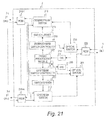
- FIG. 21 is a block diagram illustrating a configuration example of an OSW 2 according to the second embodiment of this invention.
- the OSW 2 of the second embodiment differs from the OSW 2 of the first embodiment which is described above with reference to FIG. 4 in that a downstream optical signal sent from the OLT 1 is split by an optical switch 230 instead of a splitter.
- a downstream optical signal received from the OLT 1 is distributed to the downstream switch element and the O/E converter by a splitter.
- a downstream optical signal received from the OLT 1 is delivered to any one of the downstream switch element 211 and the O/E converter 218 by the optical switch 230, which has one input port and two output ports.
- the splitter 221 couples an optical signal from the E/0 converter and an optical signal from the upstream switch element whereas, in the OSW 2 of the second embodiment, an optical signal from the E/0 converter 219 and an optical signal from the upstream switch element 212 are coupled by an optical switch 231, which has two input ports and one output port.
- an optical switch 231 which has two input ports and one output port.
- the optical switch 230 is connected to the downstream switch controller 215.
- the downstream switch controller 215 controls the switching of output ports of the optical switch 230.
- the downstream switch controller 215 periodically makes a switch to an output port of the optical switch 230 that is for a signal to be output to the downstream switch element 211, or to an output port of the optical switch 230 that is for a signal to be output to the O/E converter 218.
- the OSW 2 receives an optical switch control frame at the time when the optical switch 230 makes a switch to the output port for the O/E converter 218 in the manner described with reference to FIGS. 5 and 6 .
- the OSW 2 receives an optical signal that is a data frame destined for one of the ONUs 3 at the time when the optical switch 230 makes a switch to the output port for the downstream switch element 211 in the manner described with reference to FIGS. 5 and 6 .
- the optical switch 231 is connected to the upstream switch controller 216.
- the upstream switch controller 216 controls the switching of input ports of the optical switch 231.
- the upstream switch controller 216 periodically makes a switch to an input port of the optical switch 231 that is for a signal input from the upstream switch element 212, or to an input port of the optical switch 231 that is for a signal input from the E/0 converter.
- the OSW 2 receives an optical signal relevant to a data frame sent from one of the ONUs 3 to the OLT 1 at a time when the optical switch 231 makes a switch to the input port for the upstream switch element 212 in the manner described with reference to FIG. 7 .
- the second embodiment of this invention uses an optical switch to split an optical signal and can accordingly avoid the attenuation of an optical signal that is caused by a splitter.
Landscapes
- Engineering & Computer Science (AREA)
- Computer Networks & Wireless Communication (AREA)
- Optical Communication System (AREA)
- Small-Scale Networks (AREA)
Applications Claiming Priority (1)
| Application Number | Priority Date | Filing Date | Title |
|---|---|---|---|
| JP2008190494A JP4676517B2 (ja) | 2008-07-24 | 2008-07-24 | 光アクセスシステム、光通信路切替装置及び光回線装置 |
Publications (2)
| Publication Number | Publication Date |
|---|---|
| EP2148523A2 true EP2148523A2 (de) | 2010-01-27 |
| EP2148523A3 EP2148523A3 (de) | 2017-05-03 |
Family
ID=41258041
Family Applications (1)
| Application Number | Title | Priority Date | Filing Date |
|---|---|---|---|
| EP09165967.2A Withdrawn EP2148523A3 (de) | 2008-07-24 | 2009-07-21 | Optisches Zugriffssystem, optische Schalteinheit und optisches Leitungsendgerät |
Country Status (3)
| Country | Link |
|---|---|
| US (1) | US8401384B2 (de) |
| EP (1) | EP2148523A3 (de) |
| JP (1) | JP4676517B2 (de) |
Cited By (1)
| Publication number | Priority date | Publication date | Assignee | Title |
|---|---|---|---|---|
| US20230403485A1 (en) * | 2020-10-30 | 2023-12-14 | Nippon Telegraph And Telephone Corporation | Optical communication apparatus, optical communication system and optical communication method |
Families Citing this family (12)
| Publication number | Priority date | Publication date | Assignee | Title |
|---|---|---|---|---|
| US8855490B2 (en) * | 2007-08-31 | 2014-10-07 | Futurewei Technologies, Inc. | Backward compatible PON coexistence |
| JP5051592B2 (ja) * | 2008-07-31 | 2012-10-17 | 学校法人慶應義塾 | 光ネットワークにおける回線制御方法及び光ネットワーク |
| CN101795423A (zh) | 2009-02-04 | 2010-08-04 | 中兴通讯股份有限公司 | 无源光网络系统的时间同步方法及其同步系统 |
| US10117006B2 (en) * | 2010-03-31 | 2018-10-30 | Comcast Cable Communications, Llc | Hybrid fiber coaxial node |
| KR20120072135A (ko) * | 2010-12-23 | 2012-07-03 | 한국전자통신연구원 | 차량 진단 정보 수집 장치 및 방법 |
| US9841739B2 (en) * | 2012-06-07 | 2017-12-12 | Hitachi, Ltd. | Motion controller device and communication method therein |
| WO2017213018A1 (ja) * | 2016-06-07 | 2017-12-14 | アダマンド株式会社 | Mems光スイッチ、その駆動方法、及びmems光スイッチを備えた光スイッチモジュール |
| KR101846469B1 (ko) * | 2017-09-05 | 2018-04-09 | (주)자람테크놀로지 | 수동형 광네트워크용 저전력 장비를 위한 트랜스임피던스 증폭기 리셋 장치 및 방법 |
| US20220182740A1 (en) * | 2019-03-20 | 2022-06-09 | Sony Group Corporation | Information processing apparatus, information processing method, and communication system |
| WO2022137286A1 (ja) * | 2020-12-21 | 2022-06-30 | 日本電信電話株式会社 | 通信システム、通信装置、通信方法及びプログラム |
| JP7720516B2 (ja) * | 2021-04-14 | 2025-08-08 | Ntt株式会社 | 光通信システム、光送受信装置、及び、光通信方法 |
| EP4598048A1 (de) * | 2024-01-31 | 2025-08-06 | British Telecommunications public limited company | Faseroptisches telekommunikationsnetzwerk und verfahren zu dessen betrieb |
Citations (2)
| Publication number | Priority date | Publication date | Assignee | Title |
|---|---|---|---|---|
| JP2006246262A (ja) | 2005-03-04 | 2006-09-14 | Nec Commun Syst Ltd | 光アクセスネットワークにおける同期方法、光スイッチ装置、センタ装置、リモート装置、光アクセスシステム、光アクセスネットワーク、プログラム、及び記録媒体 |
| JP2007067948A (ja) | 2005-08-31 | 2007-03-15 | Nec Commun Syst Ltd | 光スイッチ装置、光アクセスネットワーク、光スイッチ方法およびプログラム |
Family Cites Families (6)
| Publication number | Priority date | Publication date | Assignee | Title |
|---|---|---|---|---|
| DE69823995T2 (de) * | 1998-09-23 | 2005-06-16 | Alcatel | Verfahren zur Ermittlung eines Schaltzeitpunktes |
| US7181142B1 (en) * | 2002-04-09 | 2007-02-20 | Time Warner Cable Inc. | Broadband optical network apparatus and method |
| JP4860137B2 (ja) * | 2004-11-12 | 2012-01-25 | 日本電気通信システム株式会社 | 光アクセスネットワーク方法及び光アクセスネットワーク並びに光アクセスネットワーク用光スイッチ |
| JP4708997B2 (ja) * | 2005-12-20 | 2011-06-22 | 日本電気通信システム株式会社 | 光スイッチ装置、光アクセスネットワーク、光スイッチ方法、プログラム、記録媒体 |
| JP4470963B2 (ja) * | 2007-06-01 | 2010-06-02 | 株式会社日立製作所 | ゲートウェイ装置、ont及びponシステム |
| US8208384B2 (en) * | 2007-06-26 | 2012-06-26 | Verizon Patent And Licensing Inc. | System and method for providing alarm connectivity within a network |
-
2008
- 2008-07-24 JP JP2008190494A patent/JP4676517B2/ja not_active Expired - Fee Related
-
2009
- 2009-07-16 US US12/503,884 patent/US8401384B2/en not_active Expired - Fee Related
- 2009-07-21 EP EP09165967.2A patent/EP2148523A3/de not_active Withdrawn
Patent Citations (2)
| Publication number | Priority date | Publication date | Assignee | Title |
|---|---|---|---|---|
| JP2006246262A (ja) | 2005-03-04 | 2006-09-14 | Nec Commun Syst Ltd | 光アクセスネットワークにおける同期方法、光スイッチ装置、センタ装置、リモート装置、光アクセスシステム、光アクセスネットワーク、プログラム、及び記録媒体 |
| JP2007067948A (ja) | 2005-08-31 | 2007-03-15 | Nec Commun Syst Ltd | 光スイッチ装置、光アクセスネットワーク、光スイッチ方法およびプログラム |
Non-Patent Citations (2)
| Title |
|---|
| IEICE TRANS. COMMUN., vol. E89-B, no. 11, pages 3021 - 3031 |
| IEICE TRANS. COMMUN., vol. E89-B, no. 3, pages 724 - 730 |
Cited By (2)
| Publication number | Priority date | Publication date | Assignee | Title |
|---|---|---|---|---|
| US20230403485A1 (en) * | 2020-10-30 | 2023-12-14 | Nippon Telegraph And Telephone Corporation | Optical communication apparatus, optical communication system and optical communication method |
| US12401932B2 (en) * | 2020-10-30 | 2025-08-26 | Nippon Telegraph And Telephone Corporation | Optical communication apparatus, optical communication system and optical communication method |
Also Published As
| Publication number | Publication date |
|---|---|
| JP4676517B2 (ja) | 2011-04-27 |
| JP2010028696A (ja) | 2010-02-04 |
| US20100021160A1 (en) | 2010-01-28 |
| US8401384B2 (en) | 2013-03-19 |
| EP2148523A3 (de) | 2017-05-03 |
Similar Documents
| Publication | Publication Date | Title |
|---|---|---|
| US8401384B2 (en) | Optical access system, optical switching unit and optical line terminal | |
| EP2987336B1 (de) | System und verfahren zur fotonischen umschaltung | |
| US10756841B2 (en) | System for registering an ONU to an OLT in a passive optical network system using a dedicated wavelength | |
| JP4942680B2 (ja) | 受動光網システム、光多重終端装置及び受動光網システムの通信方法 | |
| EP2415185B1 (de) | Vorrichtung für gemeinsame link-nutzung zwischen verschiedenen epons | |
| JP5051592B2 (ja) | 光ネットワークにおける回線制御方法及び光ネットワーク | |
| JP4969473B2 (ja) | 光アクセス網および光通信路切り替え制御システム | |
| EP3443693B1 (de) | Kanalbindung in passiven optischen netzwerken mit mehrfachen wellenlängen (pons) | |
| EP2245773A1 (de) | Geschütztes passives optisches kommunikationssystem | |
| US20240098392A1 (en) | Intelligent fiber to the room (fttr) gateway | |
| CN101677415A (zh) | 光网络系统数据链路切换方法、光网络单元及系统 | |
| CN100571081C (zh) | 一种无源光网络级联系统及其光线路终端 | |
| EP2101449A1 (de) | Optisches kommunikationssystem, optisches kommunikationsverfahren dafür und kommunikationseinrichtung | |
| Li et al. | Flexible low-latency metro-access converged network architecture based on optical time slice switching | |
| JP5504210B2 (ja) | 光通信システム及び光通信方法 | |
| Widjaja et al. | Simplified layering and flexible bandwidth with TWIN | |
| JP4874357B2 (ja) | 光アクセスシステム、光通信路切替装置、及び光回線装置 | |
| JP5015278B2 (ja) | 光アクセスシステム、光回線装置、及び光通信路切替装置 | |
| CN119675816B (zh) | 一种光通信装置、系统及光通信的处理方法 | |
| JP5942751B2 (ja) | Wdm/tdm−pon方式用の局側装置及び光通信ネットワークシステム | |
| CN118590792A (zh) | 光接入网中信道终端选择方法、装置及通信设备 | |
| EP3288202A1 (de) | Optisch transparentes netzwerk |
Legal Events
| Date | Code | Title | Description |
|---|---|---|---|
| PUAI | Public reference made under article 153(3) epc to a published international application that has entered the european phase |
Free format text: ORIGINAL CODE: 0009012 |
|
| 17P | Request for examination filed |
Effective date: 20091211 |
|
| AK | Designated contracting states |
Kind code of ref document: A2 Designated state(s): AT BE BG CH CY CZ DE DK EE ES FI FR GB GR HR HU IE IS IT LI LT LU LV MC MK MT NL NO PL PT RO SE SI SK SM TR |
|
| AX | Request for extension of the european patent |
Extension state: AL BA RS |
|
| PUAL | Search report despatched |
Free format text: ORIGINAL CODE: 0009013 |
|
| AK | Designated contracting states |
Kind code of ref document: A3 Designated state(s): AT BE BG CH CY CZ DE DK EE ES FI FR GB GR HR HU IE IS IT LI LT LU LV MC MK MT NL NO PL PT RO SE SI SK SM TR |
|
| AX | Request for extension of the european patent |
Extension state: AL BA RS |
|
| RIC1 | Information provided on ipc code assigned before grant |
Ipc: H04Q 11/00 20060101AFI20170330BHEP |
|
| STAA | Information on the status of an ep patent application or granted ep patent |
Free format text: STATUS: THE APPLICATION HAS BEEN WITHDRAWN |
|
| 18W | Application withdrawn |
Effective date: 20170619 |