EP2153777A1 - Ultraschallsonde und ultraschalldiagnosevorrichtung - Google Patents
Ultraschallsonde und ultraschalldiagnosevorrichtung Download PDFInfo
- Publication number
- EP2153777A1 EP2153777A1 EP08752692A EP08752692A EP2153777A1 EP 2153777 A1 EP2153777 A1 EP 2153777A1 EP 08752692 A EP08752692 A EP 08752692A EP 08752692 A EP08752692 A EP 08752692A EP 2153777 A1 EP2153777 A1 EP 2153777A1
- Authority
- EP
- European Patent Office
- Prior art keywords
- ultrasonic probe
- ultrasonic
- probe according
- insulating
- mounting board
- Prior art date
- Legal status (The legal status is an assumption and is not a legal conclusion. Google has not performed a legal analysis and makes no representation as to the accuracy of the status listed.)
- Withdrawn
Links
- 239000000523 sample Substances 0.000 title claims abstract description 108
- 238000003745 diagnosis Methods 0.000 title claims abstract description 33
- 230000005855 radiation Effects 0.000 claims abstract description 5
- 238000009429 electrical wiring Methods 0.000 claims description 14
- 239000000945 filler Substances 0.000 claims description 11
- VYPSYNLAJGMNEJ-UHFFFAOYSA-N Silicium dioxide Chemical compound O=[Si]=O VYPSYNLAJGMNEJ-UHFFFAOYSA-N 0.000 claims description 4
- 229910052814 silicon oxide Inorganic materials 0.000 claims description 4
- 230000005540 biological transmission Effects 0.000 description 23
- 239000000463 material Substances 0.000 description 10
- 238000000034 method Methods 0.000 description 7
- 230000008878 coupling Effects 0.000 description 6
- 238000010168 coupling process Methods 0.000 description 6
- 238000005859 coupling reaction Methods 0.000 description 6
- 239000000565 sealant Substances 0.000 description 6
- 239000004065 semiconductor Substances 0.000 description 5
- 230000005684 electric field Effects 0.000 description 4
- 229920005989 resin Polymers 0.000 description 4
- 239000011347 resin Substances 0.000 description 4
- 238000000926 separation method Methods 0.000 description 4
- XUIMIQQOPSSXEZ-UHFFFAOYSA-N Silicon Chemical compound [Si] XUIMIQQOPSSXEZ-UHFFFAOYSA-N 0.000 description 3
- 239000003990 capacitor Substances 0.000 description 3
- 239000000470 constituent Substances 0.000 description 3
- 238000004519 manufacturing process Methods 0.000 description 3
- 230000008569 process Effects 0.000 description 3
- 229910052710 silicon Inorganic materials 0.000 description 3
- 239000010703 silicon Substances 0.000 description 3
- 230000002411 adverse Effects 0.000 description 2
- 230000008859 change Effects 0.000 description 2
- 230000007797 corrosion Effects 0.000 description 2
- 238000005260 corrosion Methods 0.000 description 2
- 229910010272 inorganic material Inorganic materials 0.000 description 2
- 239000011147 inorganic material Substances 0.000 description 2
- 238000005459 micromachining Methods 0.000 description 2
- 230000001681 protective effect Effects 0.000 description 2
- 239000004698 Polyethylene Substances 0.000 description 1
- 239000004809 Teflon Substances 0.000 description 1
- 229920006362 Teflon® Polymers 0.000 description 1
- BZHJMEDXRYGGRV-UHFFFAOYSA-N Vinyl chloride Chemical compound ClC=C BZHJMEDXRYGGRV-UHFFFAOYSA-N 0.000 description 1
- 239000000853 adhesive Substances 0.000 description 1
- 230000001070 adhesive effect Effects 0.000 description 1
- 230000004075 alteration Effects 0.000 description 1
- 230000008901 benefit Effects 0.000 description 1
- 239000008280 blood Substances 0.000 description 1
- 210000004369 blood Anatomy 0.000 description 1
- 238000005234 chemical deposition Methods 0.000 description 1
- 150000001875 compounds Chemical class 0.000 description 1
- 238000000151 deposition Methods 0.000 description 1
- 230000008021 deposition Effects 0.000 description 1
- 230000000694 effects Effects 0.000 description 1
- 230000005611 electricity Effects 0.000 description 1
- 238000012986 modification Methods 0.000 description 1
- 230000004048 modification Effects 0.000 description 1
- 238000000465 moulding Methods 0.000 description 1
- 238000005289 physical deposition Methods 0.000 description 1
- 229920003223 poly(pyromellitimide-1,4-diphenyl ether) Polymers 0.000 description 1
- -1 polyethylene Polymers 0.000 description 1
- 229920000573 polyethylene Polymers 0.000 description 1
- 229920002635 polyurethane Polymers 0.000 description 1
- 239000004814 polyurethane Substances 0.000 description 1
- 150000003377 silicon compounds Chemical class 0.000 description 1
- 229920002379 silicone rubber Polymers 0.000 description 1
- 230000000087 stabilizing effect Effects 0.000 description 1
- BFKJFAAPBSQJPD-UHFFFAOYSA-N tetrafluoroethene Chemical compound FC(F)=C(F)F BFKJFAAPBSQJPD-UHFFFAOYSA-N 0.000 description 1
Images





Classifications
-
- B—PERFORMING OPERATIONS; TRANSPORTING
- B06—GENERATING OR TRANSMITTING MECHANICAL VIBRATIONS IN GENERAL
- B06B—METHODS OR APPARATUS FOR GENERATING OR TRANSMITTING MECHANICAL VIBRATIONS OF INFRASONIC, SONIC, OR ULTRASONIC FREQUENCY, e.g. FOR PERFORMING MECHANICAL WORK IN GENERAL
- B06B1/00—Methods or apparatus for generating mechanical vibrations of infrasonic, sonic, or ultrasonic frequency
- B06B1/02—Methods or apparatus for generating mechanical vibrations of infrasonic, sonic, or ultrasonic frequency making use of electrical energy
- B06B1/0292—Electrostatic transducers, e.g. electret-type
Definitions
- the present invention relates to an ultrasonic probe and an ultrasonic diagnosis device for photographing a diagnosis image.
- An ultrasonic diagnosis device is a device for photographing a diagnosis image based on a reflection echo signal output from an ultrasonic probe.
- a plurality of ultrasonic vibrators is arranged in the ultrasonic probe.
- the ultrasonic vibrator converts a driving signal into an ultrasonic wave, transmits the ultrasonic wave to a subject, and receives and converts a reflection echo signal generated from the subject into an electrical signal.
- the cMUT is a superfine capacitive ultrasonic vibrator manufactured by a semiconductor micromachining process.
- an ultrasonic probe which is capable of reducing manufacturing cost and improving image quality by manufacturing a vibrator cell by a semiconductor manufacturing process using a board of an inorganic material, forming a base plate of a resin material in the vibrator cell, and removing the board of the inorganic material is suggested (see Patent Document 1).
- a DC voltage is applied to a lower electrode as a bias voltage with respect to a silicon board of the cMUT and an AC high-frequency voltage is applied to an upper electrode as a driving signal with respect to the lower electrode.
- the upper electrode is not a ground layer having a ground potential.
- electrical leakage from the cMUT chip may be generated and the electrical safety for an operator who operates the cMUT probe while grasping a casing portion (case) is insufficient.
- An object of the present invention is to provide an ultrasonic probe and an ultrasonic diagnosis device capable of improving electrical safety for an operator.
- an ultrasonic probe including: a Capacitive Micromachined Ultrasonic Transducer (cMUT) chip having a plurality of vibration elements to transmit or receive an ultrasonic wave; a mounting board on which electrical parts for controlling the vibration elements are mounted; an electrical wiring portion to connect the mounting board and the cMUT chip; and a casing portion for storing the cMUT chip, the mounting board and the electrical wiring portion, wherein an insulating portion is provided between the mounting board and the casing portion.
- cMUT Capacitive Micromachined Ultrasonic Transducer
- the insulating layer is provided between the mounting board and the casing portion such as a case.
- the insulating layer is provided on the surface of the electrical wiring portion or the inner surface of the casing portion.
- the electrical wiring portion is a flexible printed circuit connected to the cMUT chip.
- the electrical parts such as an electronic circuit, a resistor or a capacitor are mounted on the mounting board.
- the cMUT chip, the electrical wiring portion and the mounting board are stored in a closed space formed by a ground layer having a ground potential.
- the ground layer is a conductive film formed on an ultrasonic wave radiation side of the cMUT chip, a conductive member provided along a surface of the electrical wiring portion or a conductive film formed along an inner surface of the casing portion.
- the conductive members or the conductive films are electrically connected so as to be connected to ground on the body side of the ultrasonic diagnosis device.
- the main components or the body circuits of the ultrasonic probe are contained in a closed space having a ground potential so as to be electrically shielded from the outside, it is possible to prevent influence of an electromagnetic wave from the inside to the outside or from the outside to the inside. In addition, it is possible to improve electrical safety of the ultrasonic probe for the operator.
- a filler may be filled in a portion or all of the internal space of the casing portion.
- a filler By filling the filler in the overall internal space of the casing portion, it is possible to prevent corrosion of the internal constituent member.
- an ultrasonic diagnosis device including the ultrasonic probe according to the first invention.
- Fig. 1 is a view showing the configuration of the ultrasonic diagnosis device 1.
- the ultrasonic diagnosis device 1 includes an ultrasonic probe 2, transmission/reception separation means 3, transmission means 4, bias means 6, reception means 8, phasing/adding means 10, image processing means 12, display means 14, control means 16, and operation means 18.
- the ultrasonic probe 2 is a device which is brought into contact with a subject so as to transmit or receive an ultrasonic wave to or from the subject.
- the ultrasonic wave is emitted from the ultrasonic probe 2 to the subject, and a reflection echo signal generated from the subject is received by the ultrasonic probe 2.
- the transmission means 4 is a device for supplying an AC high-frequency voltage as a driving signal.
- the bias means 6 is a device for applying a DC voltage as a bias voltage.
- the reception means 8 is a device for receiving the reflection echo signal output from the ultrasonic probe 2. The reception means 8 also performs an analog-to-digital converting process with respect to the received reflection echo signal.
- the transmission/reception separation means 3 switches and separates transmission and reception such that the driving signal is sent from the transmission means 4 to the ultrasonic probe 2 at the time of transmission and the reception signal is sent from the ultrasonic probe 2 to the reception means 8 at the time of reception.
- the phasing/adding means 10 is a device for phasing and adding the received reflection echo signal.
- the image processing means 12 is a device for configuring a diagnosis image (for example, a tomographic image or a blood stream image) based on the phased added reflection echo signal.
- the display means 14 is a display device for displaying the image-processed diagnosis image.
- the control means 16 is a device for controlling the above-described components.
- the operation means 18 is a device for providing an instruction to the control means 16.
- the operation means 18 is, for example, an input device such as a track ball, a keyboard, a mouse or the like.
- Fig. 2 is a view showing the configuration of the ultrasonic probe 2.
- Fig. 2 is a partial cutout perspective view of the ultrasonic probe 2.
- the ultrasonic probe 2 has a cMUT chip 20.
- the cMUT chip 20 is a one-dimensional array type vibrator group in which a plurality of vibrators 21-1, vibrators 21-2, ⁇ is arranged in a stripe shape.
- a plurality of vibration elements 22 is arranged in the vibrators 21-1, the vibrators 21-2, ⁇
- a vibration group having another shape such as a two-dimensional array type or convex type vibration group, may be used.
- a backing layer 23 is provided on a rear surface side of the cMUT chip 20.
- An acoustic lens 26 is provided on an ultrasonic wave emission side of the cMUT chip 20.
- the cMUT chip 20 and the backing layer 23 are received in a case 25.
- the cMUT chip 20 generates and transmits an ultrasonic wave to the subject based on the driving signal from the transmission means 4 and the bias voltage from the bias means 6.
- the reception means 8 converts the ultrasonic wave generated from the subject into an electrical signal and receives the electrical signal as the reflection echo signal.
- the backing layer 23 absorbs the propagation of the ultrasonic wave emitted from the cMUT chip 20 to the rear surface side so as to suppress excessive vibration.
- the acoustic lens 26 is a lens for converging an ultrasonic beam transmitted from the cMUT chip 20.
- the curvature of the acoustic lens 26 is determined based on one focal length.
- a matching layer may be provided between the acoustic lens 26 and the cMUT chip 20.
- the matching layer is a layer for matching acoustic impedance of the cMUT chip 20 and the subject so as to improve transmission efficiency of the ultrasonic wave.
- Fig. 3 is a view showing the configuration of the vibrator 21.
- Upper electrodes 28 of the vibration element 22 are connected for each of the vibrators 21 divided in a long-axis direction X. That is, an upper electrode 28-1, an upper electrode 28-2, ⁇ are arranged in parallel in the long -axis direction X.
- Lower electrodes 27 of the vibration element 22 are connected for each of sections divided in a short-axis direction Y. That is, a lower electrode 27-1, a lower electrode 27-2, ⁇ are arranged in parallel in the short-axis direction Y.
- Fig. 4 is a view showing the configuration of the vibration element 22.
- Fig. 4 is a cross-sectional view of one vibration element 22.
- the vibration element 22 includes a board 30, a film body 31, a frame body 32, a film body 33, the upper electrode 28 and the lower electrode 27.
- the vibration element 22 is formed by micromachining according to a semiconductor process.
- the vibration element 22 corresponds to one element of the cMUT.
- the board 30 is a semiconductor board such as a silicon board.
- the film body 33 and the frame body 32 are formed of a semiconductor compound such as a silicon compound.
- the film body 33 is provided on the ultrasonic wave emission side of the frame body 32.
- the upper electrode 28 is provided between the film body 33 and the frame body 32.
- the lower electrode 27 is provided in the film body 31 formed on the board 30.
- An internal space 34 partitioned by the frame body 32 and the film body 31 is in a vacuum state or is filled with predetermined gas.
- the upper electrode 28 and the lower electrode 27 are connected to the transmission means 4 and the bias means 6, respectively.
- the DC bias voltage Va is applied to the vibration element 22 through the upper electrode 28 and the lower electrode 27 and an electrical field is generated by the bias voltage Va.
- the film body 33 is tensioned by the generated electrical field to obtain a predetermined electromechanical coupling coefficient Sa.
- the driving signal is supplied from the transmission means 4 to the upper electrode 28, the ultrasonic wave is emitted from the film body 33 based on the electromechanical coupling coefficient Sa.
- the electromechanical coupling coefficient becomes ⁇ Sa ⁇ Sb. ⁇
- the film body 33 is excited by the reflection echo signal generated from the subject such that the capacitance of the internal space 34 is changed. Based on a change in capacitance of the internal space 34, the electrical signal is detected through the upper electrode 28.
- the electromechanical coupling coefficient of the vibration element 22 is determined by a tension degree of the film body 33. Accordingly, if the tension degree of the film body 33 is controlled by changing the level of the bias voltage applied to the vibration element 22, it is possible to change sound pressure (for example, amplitude) of the ultrasonic wave emitted from the vibration element 22 even when the driving signal having the same amplitude is input.
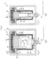
- Fig. 5 is a view showing the ultrasonic probe 2 according to a first embodiment.
- Fig. 5(a) is a cross-sectional view of a long-axis direction X.
- Fig. 5(b) is a cross-sectional view of a short-axis direction Y.
- Fig. 5(a) is a cross-sectional view of line C-C of Fig. 5(b)
- Fig. 5(b) is a cross-sectional view of line B-B of Fig. 5(a).
- Fig. 5(b) corresponds to a cross-sectional view of a plane A of the ultrasonic probe 2 of Fig. 2 .
- the ultrasonic probe 2 is connected to the body of the ultrasonic diagnosis device 1 through a cable 44.
- the acoustic lens 26 is provided on the ultrasonic wave emission side of the cMUT chip 20.
- the backing layer 23 is adhered on the rear surface side of the cMUT chip 20.
- a Flexible Printed Circuit (FPC) 41 and a FPC 42 are provided along the upper surface periphery and the four side surfaces of the backing layer 23. The FPC 41 and the FPC 42 are adhered to the upper surface periphery of the backing layer 23 in the short-axis direction Y and the long-axis direction X.
- FPC Flexible Printed Circuit
- the FPC 41 and the FPC 42 are connected to the mounting board 43 through a connector 51 and a connector 52, respectively.
- a conducting circuit between each of the terminals of the FPC 41 and the FPC 42 and the cable 44 is provided on the mounting board 43.
- the wiring (bias) from the FPC 41 is connected to a coaxial cable 57 through a connector 53 of the mounting board 43.
- the wiring (signal) from the FPC 42 is connected to a coaxial cable 58 through the connector 53 of the mounting board 43.
- a conductive film 61 is formed along an inner surface and an outer surface of the acoustic lens 26.
- the conductive film 61 is, for example, a Cu film formed by deposition.
- an insulating film may be formed together with the conductive film 61.
- Two insulating films may be formed with the conductive film 61 interposed therebetween.
- An insulating member 62 and a conductive member 63 are provided along the surface of the FPC 41 and the FPC 42.
- the insulating member 62 is a member having an insulating property.
- the insulating member is, for example, an insulating tape formed of silicon oxide or paraxylylene.
- the conductive member 63 is a member having conductivity.
- the conductive member 63 is, for example, a Cu tape.
- the conductive film 61 and the conductive member 63 are connected through a conductive member 64.
- the conductive member 64 is a high-reliable high-rigidity conductive member which is hard to damage compared with the conductive film 61.
- the conductive member 64 is, for example, a Cu tape.
- the conductive member 64 is fixed to the conductive film 61 of the outer side surface of the acoustic lens 26 and the conductive member 63 provided on the surface of the FPC 41 or the FPC 42.
- the conductive member 63 is connected to a coaxial cable 55 (shield line).
- the coaxial cable 55, the coaxial cable 57 and the coaxial cable 58 are bundled by the cable 44 so as to be connected to the body of the ultrasonic diagnosis device 1.
- the case 25 is provided on the four surface side of the ultrasonic probe 2.
- the case 25 is fixed to the four surface side of the acoustic lens 26.
- An operator grasps the case 25 and operates the ultrasonic probe 2.
- a sealant 65 is filled in a gap between the case 25 and the acoustic lens 26.
- a sealant 60 is filled in a gap between the case 25 and the cable 44.
- a filler 66 is filled between the acoustic lens 26 and the case 25.
- the upper end of the case 25 is located above the cMUT chip 20. Accordingly, even when an unexpected state such as falling of the ultrasonic probe 2 occurs, it is possible to prevent direct impact so as to protect the cMUT chip 20.
- Fig. 6 is a view showing electrical connection between the FPC and the cMUT chip.
- the FPC 41, the FPC 42 and the cMUT chip 20 are electrically connected through a wire 47 and a wire 48, respectively.
- the wire 47 and the wire 48 are connected by a wire bonding method.
- An Au wire or the like may be used as the wire 47 and the wire 48.
- the lower electrode 27 of the cMUT chip 20 and a terminal 45 of the FPC 41 are connected by the wire 47
- the upper electrode 28 of the cMUT chip 20 and a terminal 46 of the FPC 42 are connected by the wire 48.
- a photo-curable resin 49 is filled in the periphery of the wire 47 and the wire 48 such that a connection portion is sealed.
- Fig. 7 is a view showing a connector 70 used for connection with the mounting board 43.
- a connector 70 includes a pin connector 71 and a socket 72.
- the pin connector 71 is provided on an end of the FPC 41.
- Pins 73 which are protrusion-shaped electrodes are provided on the pin connector 71.
- the socket 72 is provided on an end of the mounting board 43. Holes 74 corresponding to the pins 73 are provided in the socket 72.
- the pin connector 71 is fitted into the socket 72 such that the pins 73 are inserted into the holes 74, thereby electrically connecting the FPC 41 and the mounting board 43.
- the connector 70 of Fig. 7 may be used as the connector 51, the connector 52 and the connector 53 of Fig. 5 , and another connector may be used if connection with the mounting board 43 is possible.
- a connector in which a terminal exposed from the end of the FPC 41 or the FPC 42 is directly inserted into the socket of the mounting board 43 may be used.
- Fig. 8 is a schematic view showing electrical connection between the ultrasonic probe 2 and the body of the ultrasonic diagnosis device 1.
- the ultrasonic probe 2 and the body of the ultrasonic diagnosis device 1 are connected through the cable 44.
- the cable 44 has the plurality of coaxial cable 55, coaxial cable 57 and coaxial cable 58.
- the lower electrode 27 of the cMUT chip 20 is connected to the coaxial cable 57 through the FPC 41 and the mounting board 43.
- the coaxial cable 57 is connected to a wiring 103 in the body of the ultrasonic diagnosis device 1.
- the wiring 103 is connected to the bias means 6.
- the number of coaxial cables 57 is equal to the number of lower electrodes 27 which are commonly placed in the cMUT chip 20.
- the upper electrode 28 of the cMUT chip 20 is connected to the coaxial cable 58 through the FPC 42 and the mounting board 43.
- the coaxial cable 58 is connected to a wiring 104 in the body of the ultrasonic diagnosis device 1.
- the wiring 104 is connected to a reception amplifier 108 and the transmission means 4 in the reception means 8 through the transmission/reception separation means 3.
- the number of coaxial cables 58 is equal to the number of upper electrodes 28 which are commonly placed in the cMUT chip 20.
- a resistor 106 is placed between the wiring 104 and the wiring 105.
- the wiring 105 is connected to ground 107.
- the resistor 106 is a resistor element for stabilizing the DC potential of the upper electrode 28 to a ground potential.
- Bias means 6 is placed between the wiring 103 and the wiring 105.
- the bias means 6 generates a potential difference between the upper electrode 28 and the lower electrode 27.
- the transmission means 4 applies an AC high-frequency voltage to the upper electrode 28 as the driving signal.
- the conductive film 61 of the ultrasonic probe 2 is connected to the coaxial cable 55 through the conductive member 63.
- the conductive member 63 is formed so as to cover the internal devices (the FPC 41, the FPC 42 and the mounting board 43) of the ultrasonic probe 2.
- the conductive member 63 is connected to the wiring 101 in the body of the ultrasonic diagnosis device 1 through the coaxial cable 55.
- the wiring 101 is formed so as to cover the internal circuit (the wiring 104, the wiring 103, the resistor 106 or the like) in the body of the ultrasonic diagnosis device 1.
- the wiring 101 is connected to ground 102.
- the conductive film 61, the conductive member 63, the coaxial cable 55, the wiring 101 and ground 102 form a protective circuit.
- This protective circuit prevents an external electromagnetic wave from entering the body of the ultrasonic diagnosis device 1 and the internal circuit of the ultrasonic probe 2 and prevents electricity generated in the body of the ultrasonic diagnosis device 1 and the ultrasonic probe 2 from being discharged to the outside.
- the insulating member 62 is provided between the case 25 and the ultrasonic probe along the FPC 41 and the FPC 42. Since electrical leakage from the internal device of the ultrasonic probe 2 is prevented, it is possible to improve electrical safety of the ultrasonic probe 2 for the operator.
- a material having a high insulating property and excellent heat resistance is used as the insulating member 62.
- a tape material or a sheet material having excellent insulating property and heat resistance such as kapton tape, TEFLON (registered trademark) material, vinyl chloride resin, polyurethane, polyethylene or the like, is used as the insulating member 62.
- a closed space having a ground potential is formed by the conductive film 61, the conductive member 63, the coaxial cable 55, the wiring 101 of the body device and ground 102. That is, since the main components or the body circuits of the ultrasonic probe 2 are contained in the closed space having the ground potential, it is possible to prevent the influence due to the unnecessary external wave or to prevent an external device from being adversely affected by the electromagnetic wave generated by the ultrasonic probe 2. Even when the case 25 is damaged, the ground potential of the conductive member 63 prevents an electric shock thus improving the electrical safety of the ultrasonic probe for the operator.
- the conductive film 61 is provided on the ultrasonic wave radiation side of the cMUT chip 20 as a ground layer. Accordingly, even when the acoustic lens 26 is damaged, the ground potential of the conductive film 61 prevents an electric shock thus improving the electrical safety of the ultrasonic probe for the operator.
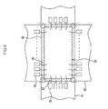
- Fig. 9 is a view showing an ultrasonic probe 2a according to the second embodiment.
- Fig. 9(a) is a cross-sectional view of a long-axis direction X.
- Fig. 9(b) is a cross-sectional view of a short-axis direction Y.
- Fig. 9(a) is a cross-sectional view of line E-E of Fig. 9(b)
- Fig. 9(b) is a cross-sectional view of line D-D of Fig. 9(a).
- Fig. 9(b) corresponds to a cross-sectional view of a plane A of the ultrasonic probe 2 of Fig. 2 .
- a conductive film 63a is formed along an inner surface of the case 25 in the second embodiment.
- the conductive film 61 and the conductive film 63a are connected through a conductive member 64a.
- the conductive member 64a of Fig. 9 is equal to the conductive member 64 of Fig. 5 .
- the conductive member 64a is fixed to the conductive film 61 of the outer side surface of the acoustic lens 26 and the conductive film 63a formed on the inner surface of the case 25.
- an insulating member 62a is provided along the inner surface of the case 25. Similar to the first embodiment, since electrical leakage from the internal device of the ultrasonic probe 2a is prevented, it is possible to improve electrical safety of the ultrasonic probe 2a for the operator.
- the conductive film 63a is formed along the inner surface of the case 25, the main components or the body circuits of the ultrasonic probe 2a are contained in the closed space having the ground potential similar to the first embodiment. Accordingly, it is possible to prevent influence due to an unnecessary external wave or prevent an external device from being adversely affected by the electromagnetic wave generated by the ultrasonic probe 2a.
- Fig. 10 is a view showing an ultrasonic probe 2b according to the third embodiment.
- Fig. 10(a) is a cross-sectional view of a long-axis direction X.
- Fig. 10(b) is a cross-sectional view of a short-axis direction Y.
- Fig. 10(a) is a cross-sectional view of line G-G of Fig. 10(b), and
- Fig. 10(b) is a cross-sectional view of line F-F of Fig. 10(a).
- Fig. 10(b) corresponds to a cross-sectional view of a plane A of the ultrasonic probe 2 of Fig. 2 .
- a filler 66b is filled in an overall space of the case 25 in the third embodiment.
- An inlet 68 is provided in the case 25 in advance.
- the filler 66b is injected from the inlet 68 into the overall internal space of the case 25 after assembling the ultrasonic probe 2b. After injecting the filler 66b, the inlet 68 is sealed by a sealant 69.
- an airtight cover may be provided on the inlet 68.
- the filler 66b is filled in the overall internal space of the case 25, it is possible to prevent corrosion of the internal constituent member. It is possible to improve impact resistance or insulating property and to improve safety of the ultrasonic probe 2b. In addition, it is possible to prevent deformation of the case 25 or to reduce the weight thereof.
- the material of the filler 66b has a light weight, an impact resistance or an insulating property.
- silicon-based resin may be used as the filler 66b.
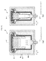
- Fig. 11 is a view showing an ultrasonic probe 2c according to the fourth embodiment.
- Fig. 11(a) is a cross-sectional view of a long-axis direction X.
- Fig. 11(b) is a cross-sectional view of a short-axis direction Y.
- Fig. 11(a) is a cross-sectional view of line H-H of Fig. 11(b)
- Fig. 11(b) is a cross-sectional view of line I-I of Fig. 11(a).
- Fig. 11(b) corresponds to a cross-sectional view of a plane A of the ultrasonic probe 2 of Fig. 2 .
- an insulating layer is provided so as to cover the overall periphery of the electrical wiring portion and the mounting board in the fourth embodiment.
- An insulating film 80 and the conductive film 61 are formed on the inner surface (concave portion) of the acoustic lens 26.
- the insulating film 80 is deposited along the inner surface of the acoustic lens 26.
- the conductive film 61 is deposited on the deposited insulating film 80.
- the conductive film 61 is, for example, a Cu film.
- two insulating films 80 may be formed with the conductive film 61 interposed therebetween.
- An insulating film 81 is adhered to the ultrasonic transmission/reception surface of the cMUT chip 20 through an adhesive.
- the insulating film 81 may be deposited on the cMUT chip 20.
- the insulating film 81 is formed of a material which scarcely influences ultrasonic transmission/reception, such as a silicon oxide or paraxylylene insulating film.
- the insulating film 81 adhered to the ultrasonic transmission/reception surface of the cMUT chip 20 covers the wire 47 and the wire 48 for connecting the cMUT chip 20 and the FPC 41, and the FPC 41 on the ultrasonic transmission/reception surface.
- the insulating film 81 covers the FPC 41 bent downward from the ultrasonic transmission/reception surface. That is, the insulating film 81 is formed so as to cover the periphery such as the cMUT chip 20 and the FPC 41.
- the insulating film 81 is connected to the insulating member 62 on the FPC 41.
- the insulating member 62 is a member having an insulating property.
- the insulating member 62 is, for example, an insulating tape formed of silicon oxide or paraxylylene.
- the insulating member 62 covers the FPC 41 bent downward from the ultrasonic transmission/reception surface of the FPC 41.
- the insulating member 62 covers the mounting board 43, on which the electrical parts 54 such as a resistor or a capacitor are mounted, from the side to the bottom thereof.
- the conductive film 61 and the conductive member 63 are connected through the conductive member 64.
- the conductive member 63 and the conductive member 64 are high-reliable high-rigidity conductive members which are hard to damage compared with the conductive film 61.
- the conductive member 63 and the conductive member 64 are, for example, Cu tapes.
- the conductive member 64 is fixed to the conductive film 61 of the inner side surface of the acoustic lens 26 and the conductive member 63 provided on the outer surface of the insulating member 62.
- the conductive member 63 is connected to the coaxial cable 55 (shield line).
- the coaxial cable 55, the coaxial cable 57 and the coaxial cable 58 are bundled through the cable 44 so as to be connected to the body of the ultrasonic diagnosis device 1.
- the case 25 is provided on the four side surfaces of the ultrasonic probe 2.
- the case 25 is fixed to the four side surfaces of the acoustic lens 26.
- the operator grasps the case 25 and operates the ultrasonic probe 2.
- a sealant 65 is filled in a gap between the case 25 and the acoustic lens 26.
- a sealant 60 is filled in a gap between the case 25 and the cable 44.
- a charging material 66 is filled between the acoustic lens 26 and the case 25.
- the upper end of the case 25 is located above the cMUT chip 20. Accordingly, even when an unexpected state such as falling of the ultrasonic probe 2 occurs, it is possible to prevent direct impact so as to protect the cMUT chip 20.
- the film thickness of the conductive layer is about 0.1 ⁇ m and the film thickness of the insulating layer is about 1 ⁇ m.
Landscapes
- Engineering & Computer Science (AREA)
- Mechanical Engineering (AREA)
- Ultra Sonic Daignosis Equipment (AREA)
- Transducers For Ultrasonic Waves (AREA)
- Investigating Or Analyzing Materials By The Use Of Ultrasonic Waves (AREA)
Applications Claiming Priority (2)
| Application Number | Priority Date | Filing Date | Title |
|---|---|---|---|
| JP2007141408 | 2007-05-29 | ||
| PCT/JP2008/058821 WO2008146600A1 (ja) | 2007-05-29 | 2008-05-14 | 超音波探触子及び超音波診断装置 |
Publications (2)
| Publication Number | Publication Date |
|---|---|
| EP2153777A1 true EP2153777A1 (de) | 2010-02-17 |
| EP2153777A4 EP2153777A4 (de) | 2016-10-12 |
Family
ID=40074867
Family Applications (1)
| Application Number | Title | Priority Date | Filing Date |
|---|---|---|---|
| EP08752692.7A Withdrawn EP2153777A4 (de) | 2007-05-29 | 2008-05-14 | Ultraschallsonde und ultraschalldiagnosevorrichtung |
Country Status (5)
| Country | Link |
|---|---|
| US (1) | US8551003B2 (de) |
| EP (1) | EP2153777A4 (de) |
| JP (1) | JP5426371B2 (de) |
| CN (1) | CN101677803B (de) |
| WO (1) | WO2008146600A1 (de) |
Families Citing this family (27)
| Publication number | Priority date | Publication date | Assignee | Title |
|---|---|---|---|---|
| US9730908B2 (en) | 2006-08-24 | 2017-08-15 | University Of Tennessee Research Foundation | SARMs and method of use thereof |
| KR101214458B1 (ko) * | 2010-01-18 | 2012-12-21 | 주식회사 휴먼스캔 | 초음파 프로브 |
| KR101173276B1 (ko) * | 2010-01-18 | 2012-08-13 | 주식회사 휴먼스캔 | 초음파 프로브 |
| EP2591731B1 (de) * | 2011-05-13 | 2014-04-30 | Olympus Medical Systems Corp. | Ultraschallwandlereinheit und ultraschallendoskop |
| JP5981998B2 (ja) * | 2011-09-26 | 2016-08-31 | コーニンクレッカ フィリップス エヌ ヴェKoninklijke Philips N.V. | 音響レンズを持つ超音波プローブ |
| US11191435B2 (en) * | 2013-01-22 | 2021-12-07 | Seno Medical Instruments, Inc. | Probe with optoacoustic isolator |
| US10433732B2 (en) | 2011-11-02 | 2019-10-08 | Seno Medical Instruments, Inc. | Optoacoustic imaging system having handheld probe utilizing optically reflective material |
| US20130289381A1 (en) | 2011-11-02 | 2013-10-31 | Seno Medical Instruments, Inc. | Dual modality imaging system for coregistered functional and anatomical mapping |
| US9733119B2 (en) | 2011-11-02 | 2017-08-15 | Seno Medical Instruments, Inc. | Optoacoustic component utilization tracking |
| US9814394B2 (en) | 2011-11-02 | 2017-11-14 | Seno Medical Instruments, Inc. | Noise suppression in an optoacoustic system |
| US9743839B2 (en) | 2011-11-02 | 2017-08-29 | Seno Medical Instruments, Inc. | Playback mode in an optoacoustic imaging system |
| US9730587B2 (en) | 2011-11-02 | 2017-08-15 | Seno Medical Instruments, Inc. | Diagnostic simulator |
| US9757092B2 (en) | 2011-11-02 | 2017-09-12 | Seno Medical Instruments, Inc. | Method for dual modality optoacoustic imaging |
| US11287309B2 (en) | 2011-11-02 | 2022-03-29 | Seno Medical Instruments, Inc. | Optoacoustic component utilization tracking |
| CN102520032B (zh) * | 2011-12-05 | 2014-08-06 | 西安交通大学 | 一种基于cmut的生化传感器及其制备方法 |
| JP6024120B2 (ja) * | 2012-02-24 | 2016-11-09 | セイコーエプソン株式会社 | 超音波プローブ、プローブヘッド、電子機器及び診断装置 |
| JP6212870B2 (ja) * | 2013-01-28 | 2017-10-18 | セイコーエプソン株式会社 | 超音波デバイス、超音波プローブ、電子機器および超音波画像装置 |
| US9833235B2 (en) * | 2013-08-16 | 2017-12-05 | Covidien Lp | Chip assembly for reusable surgical instruments |
| JP6331396B2 (ja) * | 2014-01-06 | 2018-05-30 | セイコーエプソン株式会社 | 超音波デバイス、超音波プローブ、電子機器および超音波デバイスの製造方法 |
| JP6590601B2 (ja) | 2015-09-04 | 2019-10-16 | キヤノン株式会社 | トランスデューサユニット、トランスデューサユニットを備えた音響波用プローブ、音響波用プローブを備えた光音響装置 |
| WO2017127050A1 (en) * | 2016-01-19 | 2017-07-27 | Sound Technology Inc. | Ultrasound transducer array interconnect |
| KR102635043B1 (ko) * | 2017-11-29 | 2024-02-13 | 삼성메디슨 주식회사 | 초음파프로브 |
| JP2019209169A (ja) * | 2019-09-06 | 2019-12-12 | キヤノン株式会社 | 静電容量型トランスデューサ、及び被検体情報取得装置 |
| US11841427B2 (en) * | 2019-11-28 | 2023-12-12 | Honda Electronics Co., Ltd. | Ultrasonic-wave transmitter/receiver |
| JP7565119B2 (ja) * | 2021-10-26 | 2024-10-10 | エコー イメージング,インク. | マルチトランスデューサチップ超音波デバイス |
| US11998387B2 (en) * | 2022-01-12 | 2024-06-04 | Exo Imaging, Inc. | Multilayer housing seals for ultrasound transducers |
| JP7707960B2 (ja) * | 2022-02-22 | 2025-07-15 | コニカミノルタ株式会社 | 超音波探触子および超音波診断装置 |
Family Cites Families (14)
| Publication number | Priority date | Publication date | Assignee | Title |
|---|---|---|---|---|
| JP3671725B2 (ja) * | 1999-03-26 | 2005-07-13 | フジノン株式会社 | 超音波プローブ |
| US6258034B1 (en) * | 1999-08-04 | 2001-07-10 | Acuson Corporation | Apodization methods and apparatus for acoustic phased array aperture for diagnostic medical ultrasound transducer |
| JP4118737B2 (ja) * | 2002-06-03 | 2008-07-16 | 日本電波工業株式会社 | 超音波探触子 |
| US6831394B2 (en) * | 2002-12-11 | 2004-12-14 | General Electric Company | Backing material for micromachined ultrasonic transducer devices |
| US7285897B2 (en) * | 2003-12-31 | 2007-10-23 | General Electric Company | Curved micromachined ultrasonic transducer arrays and related methods of manufacture |
| US7692364B2 (en) * | 2004-09-16 | 2010-04-06 | Olympus Medical Systems Corporation | Ultrasonic probe |
| JP4575108B2 (ja) * | 2004-10-15 | 2010-11-04 | 株式会社東芝 | 超音波プローブ |
| JP4503423B2 (ja) | 2004-11-29 | 2010-07-14 | 富士フイルム株式会社 | 容量性マイクロマシン超音波振動子及びその製造方法、並びに、超音波トランスデューサアレイ |
| US7449821B2 (en) * | 2005-03-02 | 2008-11-11 | Research Triangle Institute | Piezoelectric micromachined ultrasonic transducer with air-backed cavities |
| JP4776344B2 (ja) * | 2005-11-04 | 2011-09-21 | 株式会社日立メディコ | 超音波探触子、超音波撮像装置 |
| US8517948B2 (en) * | 2005-11-18 | 2013-08-27 | Hitachi Medical Corporation | Ultrasound diagnostic apparatus and method of calibrating the same |
| WO2008054395A1 (en) * | 2006-11-03 | 2008-05-08 | Research Triangle Institute | Enhanced ultrasound imaging probes using flexure mode piezoelectric transducers |
| JP5009301B2 (ja) | 2006-11-08 | 2012-08-22 | 株式会社日立メディコ | 超音波探触子及びこれを用いた超音波診断装置 |
| US7808157B2 (en) * | 2007-03-30 | 2010-10-05 | Gore Enterprise Holdings, Inc. | Ultrasonic attenuation materials |
-
2008
- 2008-05-14 US US12/602,119 patent/US8551003B2/en active Active
- 2008-05-14 WO PCT/JP2008/058821 patent/WO2008146600A1/ja not_active Ceased
- 2008-05-14 JP JP2009516242A patent/JP5426371B2/ja active Active
- 2008-05-14 CN CN2008800173751A patent/CN101677803B/zh active Active
- 2008-05-14 EP EP08752692.7A patent/EP2153777A4/de not_active Withdrawn
Non-Patent Citations (1)
| Title |
|---|
| See references of WO2008146600A1 * |
Also Published As
| Publication number | Publication date |
|---|---|
| CN101677803B (zh) | 2012-07-04 |
| JP5426371B2 (ja) | 2014-02-26 |
| EP2153777A4 (de) | 2016-10-12 |
| WO2008146600A1 (ja) | 2008-12-04 |
| CN101677803A (zh) | 2010-03-24 |
| US20100154547A1 (en) | 2010-06-24 |
| JPWO2008146600A1 (ja) | 2010-08-19 |
| US8551003B2 (en) | 2013-10-08 |
Similar Documents
| Publication | Publication Date | Title |
|---|---|---|
| US8551003B2 (en) | Ultrasonic probe and ultrasonic diagnosis device | |
| CN101636112B (zh) | 超声波探头及其制造方法及超声波诊断装置 | |
| CN103181785B (zh) | 超声波探头及其制造方法 | |
| US6936008B2 (en) | Ultrasound system with cableless coupling assembly | |
| US5545942A (en) | Method and apparatus for dissipating heat from a transducer element array of an ultrasound probe | |
| US8758253B2 (en) | Ultrasonic probe and ultrasonic diagnostic apparatus using the same | |
| JP5954773B2 (ja) | 超音波プローブおよび超音波プローブの製造方法 | |
| US9184370B2 (en) | Ultrasonic transducer device, ultrasonic measurement apparatus, head unit, probe, and ultrasonic imaging apparatus | |
| US9623443B2 (en) | Ultrasonic device unit, probe, electronic device and ultrasonic imaging device | |
| CN105726060B (zh) | 超声探头设备 | |
| EP3023778B1 (de) | Kapazitiver wandler und probeninformationserfassungsvorrichtung | |
| CN104203107B (zh) | 超声波探头及信号线的连接方法 | |
| US10074795B2 (en) | Ultrasonic probe as well as electronic apparatus and ultrasonic imaging apparatus | |
| JP4376533B2 (ja) | 超音波探触子 | |
| JP2016092591A (ja) | 超音波デバイスユニット並びにプローブおよび電子機器 | |
| JP5269307B2 (ja) | 超音波探触子及び超音波診断装置 | |
| JP3380190B2 (ja) | 超音波探触子 | |
| JPH07274296A (ja) | 配列型の超音波探触子 |
Legal Events
| Date | Code | Title | Description |
|---|---|---|---|
| PUAI | Public reference made under article 153(3) epc to a published international application that has entered the european phase |
Free format text: ORIGINAL CODE: 0009012 |
|
| 17P | Request for examination filed |
Effective date: 20091229 |
|
| AK | Designated contracting states |
Kind code of ref document: A1 Designated state(s): AT BE BG CH CY CZ DE DK EE ES FI FR GB GR HR HU IE IS IT LI LT LU LV MC MT NL NO PL PT RO SE SI SK TR |
|
| AX | Request for extension of the european patent |
Extension state: AL BA MK RS |
|
| DAX | Request for extension of the european patent (deleted) | ||
| RA4 | Supplementary search report drawn up and despatched (corrected) |
Effective date: 20160908 |
|
| RIC1 | Information provided on ipc code assigned before grant |
Ipc: H04R 19/00 20060101ALI20160902BHEP Ipc: A61B 8/00 20060101ALI20160902BHEP Ipc: B06B 1/02 20060101AFI20160902BHEP |
|
| RAP1 | Party data changed (applicant data changed or rights of an application transferred) |
Owner name: HITACHI, LTD. |
|
| 17Q | First examination report despatched |
Effective date: 20180103 |
|
| STAA | Information on the status of an ep patent application or granted ep patent |
Free format text: STATUS: THE APPLICATION HAS BEEN WITHDRAWN |
|
| 18W | Application withdrawn |
Effective date: 20180220 |