EP2154607A2 - Gewindeoptimierte Multiprozessor-Architektur - Google Patents
Gewindeoptimierte Multiprozessor-Architektur Download PDFInfo
- Publication number
- EP2154607A2 EP2154607A2 EP09174901A EP09174901A EP2154607A2 EP 2154607 A2 EP2154607 A2 EP 2154607A2 EP 09174901 A EP09174901 A EP 09174901A EP 09174901 A EP09174901 A EP 09174901A EP 2154607 A2 EP2154607 A2 EP 2154607A2
- Authority
- EP
- European Patent Office
- Prior art keywords
- processors
- instruction
- processor
- thread
- instruction set
- Prior art date
- Legal status (The legal status is an assumption and is not a legal conclusion. Google has not performed a legal analysis and makes no representation as to the accuracy of the status listed.)
- Withdrawn
Links
Images


Classifications
-
- G—PHYSICS
- G06—COMPUTING OR CALCULATING; COUNTING
- G06F—ELECTRIC DIGITAL DATA PROCESSING
- G06F9/00—Arrangements for program control, e.g. control units
- G06F9/06—Arrangements for program control, e.g. control units using stored programs, i.e. using an internal store of processing equipment to receive or retain programs
- G06F9/30—Arrangements for executing machine instructions, e.g. instruction decode
- G06F9/30098—Register arrangements
- G06F9/3012—Organisation of register space, e.g. banked or distributed register file
- G06F9/30138—Extension of register space, e.g. register cache
-
- G—PHYSICS
- G06—COMPUTING OR CALCULATING; COUNTING
- G06F—ELECTRIC DIGITAL DATA PROCESSING
- G06F12/00—Accessing, addressing or allocating within memory systems or architectures
- G06F12/02—Addressing or allocation; Relocation
- G06F12/08—Addressing or allocation; Relocation in hierarchically structured memory systems, e.g. virtual memory systems
- G06F12/0802—Addressing of a memory level in which the access to the desired data or data block requires associative addressing means, e.g. caches
- G06F12/0875—Addressing of a memory level in which the access to the desired data or data block requires associative addressing means, e.g. caches with dedicated cache, e.g. instruction or stack
-
- G—PHYSICS
- G06—COMPUTING OR CALCULATING; COUNTING
- G06F—ELECTRIC DIGITAL DATA PROCESSING
- G06F15/00—Digital computers in general; Data processing equipment in general
- G06F15/76—Architectures of general purpose stored program computers
- G06F15/78—Architectures of general purpose stored program computers comprising a single central processing unit
- G06F15/7807—System on chip, i.e. computer system on a single chip; System in package, i.e. computer system on one or more chips in a single package
- G06F15/781—On-chip cache; Off-chip memory
-
- G—PHYSICS
- G06—COMPUTING OR CALCULATING; COUNTING
- G06F—ELECTRIC DIGITAL DATA PROCESSING
- G06F15/00—Digital computers in general; Data processing equipment in general
- G06F15/76—Architectures of general purpose stored program computers
- G06F15/78—Architectures of general purpose stored program computers comprising a single central processing unit
- G06F15/7839—Architectures of general purpose stored program computers comprising a single central processing unit with memory
- G06F15/7842—Architectures of general purpose stored program computers comprising a single central processing unit with memory on one IC chip (single chip microcontrollers)
- G06F15/7846—On-chip cache and off-chip main memory
-
- G—PHYSICS
- G06—COMPUTING OR CALCULATING; COUNTING
- G06F—ELECTRIC DIGITAL DATA PROCESSING
- G06F9/00—Arrangements for program control, e.g. control units
- G06F9/06—Arrangements for program control, e.g. control units using stored programs, i.e. using an internal store of processing equipment to receive or retain programs
- G06F9/30—Arrangements for executing machine instructions, e.g. instruction decode
- G06F9/30145—Instruction analysis, e.g. decoding, instruction word fields
-
- G—PHYSICS
- G06—COMPUTING OR CALCULATING; COUNTING
- G06F—ELECTRIC DIGITAL DATA PROCESSING
- G06F9/00—Arrangements for program control, e.g. control units
- G06F9/06—Arrangements for program control, e.g. control units using stored programs, i.e. using an internal store of processing equipment to receive or retain programs
- G06F9/30—Arrangements for executing machine instructions, e.g. instruction decode
- G06F9/32—Address formation of the next instruction, e.g. by incrementing the instruction counter
- G06F9/322—Address formation of the next instruction, e.g. by incrementing the instruction counter for non-sequential address
- G06F9/323—Address formation of the next instruction, e.g. by incrementing the instruction counter for non-sequential address for indirect branch instructions
-
- G—PHYSICS
- G06—COMPUTING OR CALCULATING; COUNTING
- G06F—ELECTRIC DIGITAL DATA PROCESSING
- G06F9/00—Arrangements for program control, e.g. control units
- G06F9/06—Arrangements for program control, e.g. control units using stored programs, i.e. using an internal store of processing equipment to receive or retain programs
- G06F9/30—Arrangements for executing machine instructions, e.g. instruction decode
- G06F9/38—Concurrent instruction execution, e.g. pipeline or look ahead
- G06F9/3836—Instruction issuing, e.g. dynamic instruction scheduling or out of order instruction execution
- G06F9/3851—Instruction issuing, e.g. dynamic instruction scheduling or out of order instruction execution from multiple instruction streams, e.g. multistreaming
-
- G—PHYSICS
- G06—COMPUTING OR CALCULATING; COUNTING
- G06F—ELECTRIC DIGITAL DATA PROCESSING
- G06F9/00—Arrangements for program control, e.g. control units
- G06F9/06—Arrangements for program control, e.g. control units using stored programs, i.e. using an internal store of processing equipment to receive or retain programs
- G06F9/30—Arrangements for executing machine instructions, e.g. instruction decode
- G06F9/38—Concurrent instruction execution, e.g. pipeline or look ahead
- G06F9/3867—Concurrent instruction execution, e.g. pipeline or look ahead using instruction pipelines
-
- G—PHYSICS
- G06—COMPUTING OR CALCULATING; COUNTING
- G06F—ELECTRIC DIGITAL DATA PROCESSING
- G06F9/00—Arrangements for program control, e.g. control units
- G06F9/06—Arrangements for program control, e.g. control units using stored programs, i.e. using an internal store of processing equipment to receive or retain programs
- G06F9/30—Arrangements for executing machine instructions, e.g. instruction decode
- G06F9/38—Concurrent instruction execution, e.g. pipeline or look ahead
- G06F9/3885—Concurrent instruction execution, e.g. pipeline or look ahead using a plurality of independent parallel functional units
- G06F9/3889—Concurrent instruction execution, e.g. pipeline or look ahead using a plurality of independent parallel functional units controlled by multiple instructions, e.g. MIMD, decoupled access or execute
- G06F9/3891—Concurrent instruction execution, e.g. pipeline or look ahead using a plurality of independent parallel functional units controlled by multiple instructions, e.g. MIMD, decoupled access or execute organised in groups of units sharing resources, e.g. clusters
Definitions
- Computer speed may be increased using two general approaches: increase instruction execution speed or do more instruction execution in parallel.
- increase instruction execution speed approaches the limits of electron mobility in silicon, parallelism becomes the best alternative to increasing computer speed.
- a pipeline is an instruction execution unit consisting of multiple sequential stages that successively perform a piece of an instruction's execution, such as fetch, decode, execute, store, etc.
- Several pipelines may be placed in parallel, such that program instructions are fed to each pipeline one after another until all pipelines are executing an instruction. Then the instruction filling repeats with the original pipeline.
- N pipelines are filled with instructions and executing, the performance effect is theoretically the same as an N times increase in execution speed for a single execution unit.
- pipelines encourage complex multi-state instructions.
- the exceptions to the waiting rule are applications like engine controllers, signal processors, and firewall routers. These applications are excellent candidates for parallelism acceleration due to the predefined nature of the problem sets and solution sets. A problem that requires the product ofN independent multiplications may be solved faster using N multipliers.
- the perceived performance of a general purpose computer is really its peak performance.
- the closest a general purpose computer gets to being busy is running a video game with a rapid screen refresh, compiling a large source file, or searching a database.
- the video rendering would be factored into special purpose, shading, transforming, and rendering hardware.
- One method of factoring the programming to such special purpose hardware is the use of "threads.”
- Threads are independent programs that are self contained and infrequently communicate data with other threads.
- a common use of threads is to collect data from slow realtime activity and provide the assembled results.
- a thread might also be used to render a change on a display.
- a thread may transition through thousands or millions of states before requiring further interaction with another thread. Independent threads present an opportunity for increased performance through parallelism.
- Threading is a well understood technique for factoring software programs on a single CPU. Thread level parallelism can achieve program acceleration through use of a TOMI processor.
- TOMI processor requires minimal changes to current software programming techniques. New algorithms do not need to be developed. Many existing programs may need to be recompiled, but not substantially rewritten.
- the parameters of LOAD and STORE are the source and destination.
- the power of the LOAD and STORE is the range of source and destination (for example, 4 Gbytes is a more powerful range than 256 bytes). Locality relative to the current source and destination is important for many data sets. Plus 1, minus 1 are the most useful. Increasing offsets from the current source and destination are progressively less useful.
- Branches and loops are the fundamental sequencing instructions. Instruction sequence changes based on a test is the way computers make decisions.
- Math and logic operations are the least used of the three operations. Logic operations are the fastest operations a CPU can perform and can require as little as a single logic gate delay. Math operations are more complex since higher order bits depend on the results of lower order bit operations. A 32-bit ADD can require at least 32 gate delays, even with carry lookabead. MULTIPLY using a shift and add technique can require the equivalent of 32 ADDs.
- the perfect instruction set would consist of op-codes that are large enough to select infinite possible sources, destinations, operations, and next instructions. Unfortunately the perfect instruction set op-codes would be infinitely wide and the instruction bandwidth would therefore be zero.
- Computer design for high-instruction bandwidth involves the creation of an instruction set with op-codes able to efficiently define the most common sources, destinations, operations, and next instructions with the fewest op-code bits.
- a memory bus is 64 bits wide, one could fetch a single 64-bit instruction, two 32-bit instructions, four 16-bits instructions, or eight 8-bit instructions in each memory cycle.
- a 32-bit instruction had better be twice as useful as a 16-bit instruction since it cuts the instruction bandwidth in half.
- a major objective of instruction set design is to reduce instruction redundancy.
- an optimized efficient instruction set takes advantage of the locality of both instructions and data. The easiest instruction optimizations have long since been done.
- the most likely next instruction is the sequentially next instruction in memory. Therefore instead of every instruction having a next instruction field, most instructions assume the next instruction is the current instruction + 1. It is possible to create an architecture with zero bits for source and zero bits for destination.
- Stack architecture computers are also called zero operand architectures.
- a stack architecture performs all operations based on the contents of a push down stack.
- a two operand operation would require both operands be present on the stack.
- both operands would be POP'd from the stack, the operation would be performed, and the result would be PUSH'd back on the stack.
- Stack architecture computers can have very short op-codes since the source and destination are implied as being on the stack.
- Stack architecture operation is also often redundant in ways that defy obvious optimizations. For example, each POP and PUSH operation has the potential to cause a time wasting memory operation as the stack is manipulated in memory. Furthermore, the stack operation may consume an operand that may be immediately needed for the next operation, thereby requiring operand duplication with the potential of yet another memory operation. Take for example, the operation of multiplying all the elements of a one dimensional array by 15.
- the loop counter in line 9 would require an additional parameter. In some architectures, this parameter is stored on another stack.
- the stack operation has at least 3 possible opportunities for an extra memory access due to stack operation.
- the loop control of the hypothetical register/accumulator architecture could easily be handled in a register.
- Stacks are useful for evaluating expressions and are used as such in most compilers. Stacks are also useful for nested operations such as function calls. Most C compilers implement function calls with a stack. However, without supplementing by general purpose storage, a stack architecture requires lots of extra data movement and manipulation. For optimization purposes, stack PUSH and POP operations should also be separated from math and logic operations. But as can be seen from the example above, stacks are particularly inefficient when loading and storing data repeatedly, since the array addresses are consumed by the PUSH INDIRECT and POP INDIRECT.
- the invention comprises a system comprising: (a) a plurality of parallel processors on a single chip; and (b)computer memory located on the chip and accessible by each of the processors; wherein each of the processors is operable to process a de minimis instruction set, and wherein each of the processors comprises local caches dedicated to each of at least three specific registers in the processor.
- each of the local caches is equivalent to one row of random access memory on the chip; (2) the at least three specific registers with an associated cache include an instruction register, source register, and destination register; (3) the de minimis instruction set consists of seven instructions; (4) each of the processors is operable to process a single thread; (5) an accumulator is an operand for every instruction, except an increment instruction; (6) a destination for each instruction is always an operand register; (7) three registers auto-increment and three registers auto-decrement; (8) each instruction requires only one clock cycle to complete; (9) the instruction set comprises no BRANCH instruction and no JUMP instruction; (10) each instruction is at most 8 bits in length; and (11) a single master processor is responsible for managing each of the parallel processors.
- each of the processors is operable to process a de minimis instruction set; (2) each of the processors comprises local caches dedicated to each of at least three specific registers in the processor; (3) the size of each of the local caches is equivalent to one row of random access memory on the chip; (4) the at least three specific registers include an instruction register, source register, and destination register; (5) the de minimis instruction set consists of seven instructions; (6) each of the processors is operable to process a single thread; and (7) a single master processor is responsible for managing each of the parallel processors.
- the de minimis instruction set consists of seven instructions; (2) instruction in the de minimis instruction set is at most 8 bits in length; and (3) each instruction in the de minimis instruction set is processed in one clock cycle.
- the TOMI architecture of at least one embodiment of the present invention preferably uses the minimum logic possible to operate as a general purpose computer. The most common operations are given priority. Most operations are visible, regular, and available for compiler optimization.
- the architecture is designed to be simple enough to be replicated numerous times on a single monolithic chip.
- One embodiment embeds multiple copies of the CPU monolithically with memory.
- a 32-bit CPU may be implemented in fewer than 1,500 gates, with most of the gates defining the registers. Nearly 1,000 TOMI CPUs of a preferred embodiment can be implemented using the same number of transistors as a single Intel Pentium 4.
- Each instruction preferably consists of a single 8-bit word.
- the addressing modes are:
- PC Program Counter
- a skip may be created by executing INC, PC, Execution will require two cycles, one for the current PC increment cycle to complete and one for the INC.
- a skip may be made conditional on the state of C by incrementing Register 0.
- a relative branch may be created by loading the desired offset into the ACC and then executing the ADD, PC instruction.
- a relative branch may be made conditional on the state of C by adding to Register 0.
- Forward branches are more useful than rearward branches since the location of the rearward branches necessary for loops is easily captured by saving the PC as the program steps through the top of the loop the first time.
- a more efficient forward branch than the relative branch may be created by loading the least significant bits of the branch endpoint into the ACC and then storing to the PC. Since the PC can be accessed both conditionally or unconditionally depending upon the use of Register 0 or Register 1, the forward branch may also be conditional or unconditional by the selection of the PC register (Register 0 or Register 1) as the destination operand.
- the current PC register is incremented, starting with the 7th bit.
- FIG. 2A shows the forward branch in operation.
- the top of a loop may be saved using LOADACC, PC.
- the resulting pointer to the top of the looping construct may then be stored in a register or pushed into one of the autoindexing registers.
- the pointer may be retrieved with LOADACC, EA and restored to the PC using STOREACC, PC, thereby causing a backwards loop.
- the loop may be made conditional on the state of C by storing to Register 0 thereby causing a conditional backwards loop.
- JUMPTABLE might be in low memory so its address can be created with LOADI or a LOADI following by one or more right shifts, ADD, ACC.
- each system call may be executed as follows where SPECIAL_FUNCTION is the name of an immediate operand 0-63: LOADI, SPECIAL_FUNCTION Load the system call number LOADACC, (ACC) Load the address of the system call STOREACC, PC Jump to the function
- the basic architecture does not envision a right shift operation. Should such an operation be required, the solution of a preferred embodiment is to designate one of the general purpose registers as the "right shift register.”
- a STOREACC, RIGHTSHIFT would store the ACC right shifted a single position into the "right shift register” whers its value could be read with LOADACC, RIGHTSHIFT.
- the TOMI architecture preferably features 8-bit instructions, but the data width need not be restricted.
- FIG. 4 illustrates how any width data paths from 4-32 bits are easily created. Creating larger width data handling only requires increasing the width of the register set, the internal data paths, and the ALU to the desired widths. The upper bound of the data path is only limited by the carry propagation delay of the adder and the transistor budget.
- a general purpose register may be preconfigured as all "1s” and named ALLONES.
- the operand will be assumed to be in a register named OPERAND: LOADACC, ALLONES XOR, OPERAND INC, OPERAND
- OPERAND The "2s" complement is left in OPERAND.
- a C compiler will normally maintain a stack for passing parameters to function calls.
- the S, X, or Y registers may be used as the stack pointer.
- the function call will push the parameters onto one of the autoindexing registers acting as the stack, using, for example: STOREACC, (X)+.
- STOREACC, (X)+ Upon entering the function the parameters will be POP'd into general purpose registers for use.
- the base address of the array is located in a general purpose register named ARRAY.
- ARRAY To read the Nth element in the array: LOADI, N STROREACC,X LOADACC, ARRAY ADD, X LOADACC, (X)
- ARRAY a general purpose register
- a cache is memory smaller in size and faster in access than the main memory.
- the reduced access time and the locality of program and data accesses allow cache operations to increase performance of a preferred TOMI processor for many operations.
- a cache increases parallel processing performance by increasing independence of a TOMI processor from main memory.
- the relative performance of cache to main memory and the number of cycles the TOMI processor can execute before requiring another main memory load or store to or from cache determine the amount of performance increase due to TOMI processor parallelism.
- TOMI local caches enhance the performance increase due to TOMI processor parallelism.
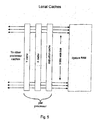
- Each TOMI processor preferably has three associated local caches, as illustrated in FIG. 5 :
- a wide bus connects the large embedded memory to the caches, so a load or store operation to the caches can occur quickly.
- a load or store of an entire cache would consist of a single memory cycle to a RAM column.
- the embedded memory will be responding to request of 63 TOMI processors, so the response time of a cache load or store for one TOMI processor may be extended while the load or store of another TOMI processor cache competes.
- Caches may be stored and loaded based on changes of the associated memory addressing registers X, Y, PC, as illustrated in FIG. 6 .
- the total width of the PC register might be 24 bits. If the PC cache is 1024 bytes, the lower 10 bits of the PC would define access within the PC cache.
- a cache load cycle would be required. The TOMI CPU associated with that PC cache would stop executing until the cache load cycle was complete and the indicated instruction could be fetched from the PC cache.
- a secondary cache may be loaded in anticipation of the cache load requirement,
- the two caches would be identical and alternately be selected and deselected based on the contents of the upper 14 bits of the PC,
- the secondary cache would become selected as the primary cache.
- the old primary cache would now become the secondary cache. Since most computer programs linearly increase in memory, one embodiment of the invention would have the secondary cache always fetching the contents of the cache contents of main memory referenced by the upper 14 bits of the current PC plus 1.
- secondary caches will reduce the time the TOMI processor must wait for memory data to be fetched from main memory when moving outside of the boundary of the current cache.
- the addition of secondary caches nearly doubles the complexity of a TOMI processor. For an optimal system, this doubling of complexity should be offset by a corresponding doubling of performance of the TOMI processor. Otherwise, two simpler TOMI processors without secondary cache can be implemented with the same transistor count.
- DSP Digital Signal Processing
- An interrupt is an event external to the normal sequential operation of a processor that causes the processor to immediately change its sequence of operation.
- a multiprocessor TOMI system only one processor possesses primary interrupt capability. All other processors run uninterrupted until they complete some assigned work and stop themselves or until they are stopped by the coordinating processor.
- I/O Input/Output
- a single processor is responsible for all interfacing to the external world.
- DMA Direct Memory Access
- immediate response to the external world in a TOMI processor system occurs via a DMA controller.
- a DMA controller when requested by an external device, transfers data from the external device to the internal data bus for writing to the system RAM, The same controller also transfers data from the system RAM to the external device when requested.
- a DMA request would have the highest priority for internal bus access.
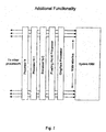
- the TOMI processor of preferred embodiments of the invention is designed to be replicated in large numbers and combined with additional processing functionality, a very wide internal bus, and system memory on a monolithic chip.
- An exemplary memory map for such a system is illustrated in FIG. 8 .
- each processor dedicates the first 32 locations (IF hex) to the local registers for that processor (see FIG. 3 ).
- the remainder of the memory map is addressable by all processors through their cache registers (see FIG. 6 ).
- the addressability of the system RAM is limited only by the width of the three registers associated with the local caches; PC, X, and Y. If the registers are 24 bits wide, the total addressability would be 4 Mbytes, but there is no upper limit.
- 64 TOMI processors are implemented monolithically with memory.
- a single master processor is responsible for managing the other 63. When one of the slave processors is idle, it is not clocking so it consumes little or no power and generates little or no heat. On initialization, only the master processor is operational. The master begins fetching and executing instructions until a time that a thread should be started. Each thread has been precompiled and loaded into memory. To start a thread, the master allocates the thread to one of the TOMI CPUs.
- the coordinating (master) processor preferably can perform the following functions:
- the coordinating processor may request a processor from the availability table. The number of the lowest processor with an available_flag set to "0" is returned. The coordinating processor may then set the available_flag associated with the available processor to "1", thereby starting the slave processor. If no processor is available, the request will return an error.
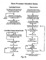
- processors may be allocated by the coordinating processor based upon a priority level associated with the requested work to be performed. Techniques to allocate resources based upon priority schemes are well-known in the art. FIG. 10 illustrates three preferred components of processor allocation; Coordinating Processor initiating operations, Slave Processor operations, and Coordinating Processor result handling through interrupt response.
- the coordinating processor When the coordinating processor detects that the done_flag is set, it may handle the slave processor's results and possibly reassign the slave processor to do new work. When the slave processor's results have been processed, the associated coordinating processor will clear the associated done_flag.
- the coordinating processor may also read the return parameters pushed on the slave processor's stack.
- the interrupt handler will handle the slave processor's results and possibly reassign the slave processor to do new work.
- the interrupt handler running on the coordinating processor will clear the associated done_flag.
- the slave processor sets its associated done_flag and saves the new start_time.
- the slave processor may continue to do work or may return to the available state.
- the slave processor may push return parameters onto its stack, followed by a stack count and set its available_flag.
- TOMI processors read and write system memory through their caches. A completely cached column is read or written at one time. Any processor may read any portion of system memory. An individual processor may lock a column of memory for its exclusive writing. This locking mechanism avoids memory writing conflicts between processors.
- FIG. 12 shows how the TOMI system RAM may be allocated in one embodiment.
- One block of system RAM holds the image capture pixels, and another block holds the processed results.
- FIG. 13 shows an exemplary floorplan for a monolithic array of 64 processors.
Landscapes
- Engineering & Computer Science (AREA)
- Theoretical Computer Science (AREA)
- Software Systems (AREA)
- General Engineering & Computer Science (AREA)
- Physics & Mathematics (AREA)
- General Physics & Mathematics (AREA)
- Computer Hardware Design (AREA)
- Multimedia (AREA)
- Microelectronics & Electronic Packaging (AREA)
- Computing Systems (AREA)
- Advance Control (AREA)
- Memory System Of A Hierarchy Structure (AREA)
- Multi Processors (AREA)
- Image Processing (AREA)
Applications Claiming Priority (2)
| Application Number | Priority Date | Filing Date | Title |
|---|---|---|---|
| US76495506P | 2006-02-03 | 2006-02-03 | |
| EP07763540A EP1979808B1 (de) | 2006-02-03 | 2007-02-05 | Gewindeoptimierte multiprozessor-architektur |
Related Parent Applications (1)
| Application Number | Title | Priority Date | Filing Date |
|---|---|---|---|
| EP07763540.7 Division | 2007-02-05 |
Publications (2)
| Publication Number | Publication Date |
|---|---|
| EP2154607A2 true EP2154607A2 (de) | 2010-02-17 |
| EP2154607A3 EP2154607A3 (de) | 2010-07-14 |
Family
ID=38345789
Family Applications (2)
| Application Number | Title | Priority Date | Filing Date |
|---|---|---|---|
| EP09174901A Withdrawn EP2154607A3 (de) | 2006-02-03 | 2007-02-05 | Gewindeoptimierte Multiprozessor-Architektur |
| EP07763540A Not-in-force EP1979808B1 (de) | 2006-02-03 | 2007-02-05 | Gewindeoptimierte multiprozessor-architektur |
Family Applications After (1)
| Application Number | Title | Priority Date | Filing Date |
|---|---|---|---|
| EP07763540A Not-in-force EP1979808B1 (de) | 2006-02-03 | 2007-02-05 | Gewindeoptimierte multiprozessor-architektur |
Country Status (10)
| Country | Link |
|---|---|
| US (1) | US8977836B2 (de) |
| EP (2) | EP2154607A3 (de) |
| JP (1) | JP4987882B2 (de) |
| KR (1) | KR101120398B1 (de) |
| CN (1) | CN101395578B (de) |
| AT (1) | ATE536585T1 (de) |
| AU (1) | AU2007212342B2 (de) |
| CA (1) | CA2642022A1 (de) |
| RU (1) | RU2427895C2 (de) |
| WO (1) | WO2007092528A2 (de) |
Families Citing this family (22)
| Publication number | Priority date | Publication date | Assignee | Title |
|---|---|---|---|---|
| RU2427895C2 (ru) | 2006-02-03 | 2011-08-27 | Рассел Х. ФИШ III | Оптимизированная для потоков многопроцессорная архитектура |
| US8984256B2 (en) * | 2006-02-03 | 2015-03-17 | Russell Fish | Thread optimized multiprocessor architecture |
| US7962553B2 (en) * | 2006-07-31 | 2011-06-14 | Hewlett-Packard Development Company, L.P. | Method and system for distribution of maintenance tasks in a multiprocessor computer system |
| US8755515B1 (en) | 2008-09-29 | 2014-06-17 | Wai Wu | Parallel signal processing system and method |
| US8407680B2 (en) * | 2008-12-16 | 2013-03-26 | International Business Machines Corporation | Operand data structure for block computation |
| US8281106B2 (en) * | 2008-12-16 | 2012-10-02 | International Business Machines Corporation | Specifying an addressing relationship in an operand data structure |
| US8458439B2 (en) * | 2008-12-16 | 2013-06-04 | International Business Machines Corporation | Block driven computation using a caching policy specified in an operand data structure |
| US8285971B2 (en) * | 2008-12-16 | 2012-10-09 | International Business Machines Corporation | Block driven computation with an address generation accelerator |
| US8327345B2 (en) * | 2008-12-16 | 2012-12-04 | International Business Machines Corporation | Computation table for block computation |
| EP2396730A4 (de) * | 2009-02-13 | 2013-01-09 | Alexey Raevsky | Vorrichtungen und verfahren für optimierte parallele datenverarbeitung in multicore-datenverarbeitungssystemen |
| JP5367416B2 (ja) * | 2009-03-04 | 2013-12-11 | 光洋サーモシステム株式会社 | 搬送ロボット装置 |
| US9535876B2 (en) | 2009-06-04 | 2017-01-03 | Micron Technology, Inc. | Conditional operation in an internal processor of a memory device |
| US8527740B2 (en) * | 2009-11-13 | 2013-09-03 | International Business Machines Corporation | Mechanism of supporting sub-communicator collectives with O(64) counters as opposed to one counter for each sub-communicator |
| US9823928B2 (en) | 2011-09-30 | 2017-11-21 | Qualcomm Incorporated | FIFO load instruction |
| KR101984635B1 (ko) | 2012-07-19 | 2019-05-31 | 삼성전자주식회사 | 어플리케이션을 고속으로 처리하는 연산 처리 장치 및 방법 |
| JP6099329B2 (ja) * | 2012-08-02 | 2017-03-22 | シャープ株式会社 | 端末、基地局、通信方法および集積回路 |
| US9760511B2 (en) * | 2014-10-08 | 2017-09-12 | International Business Machines Corporation | Efficient interruption routing for a multithreaded processor |
| CN107111490A (zh) | 2014-12-19 | 2017-08-29 | 谢尔盖·阿纳托利耶维奇·格瑞斯尼 | 功能约束数据的管理系统和方法 |
| RU2612569C2 (ru) * | 2015-01-27 | 2017-03-09 | Акционерное общество "Научно-исследовательский институт Авиационного оборудования" | Способ автоматического управления избыточностью неоднородной вычислительной системы и устройство для его реализации |
| CN104699449B (zh) * | 2015-04-03 | 2017-09-29 | 中国科学院软件研究所 | 一种基于gmp的大整数加法和减法多核并行化实现方法 |
| CN111104062B (zh) * | 2019-11-22 | 2023-05-02 | 中科寒武纪科技股份有限公司 | 存储管理方法、装置和存储介质 |
| TWI768731B (zh) | 2021-02-25 | 2022-06-21 | 威盛電子股份有限公司 | 電腦系統 |
Family Cites Families (25)
| Publication number | Priority date | Publication date | Assignee | Title |
|---|---|---|---|---|
| US530890A (en) * | 1894-12-11 | Patrick fitzgibbons | ||
| DE1979808U (de) | 1967-01-12 | 1968-02-29 | Hovalwerk Ag Ospelt | Heizkessel zum verfeuern fluessiger oder gasfoermiger brennstoffe. |
| US3990054A (en) * | 1974-11-05 | 1976-11-02 | Honeywell Inc. | Microprogram organization techniques |
| US4641238A (en) * | 1984-12-10 | 1987-02-03 | Itt Corporation | Multiprocessor system employing dynamically programmable processing elements controlled by a master processor |
| SU1464168A1 (ru) * | 1987-04-23 | 1989-03-07 | Таганрогский радиотехнический институт им.В.Д.Калмыкова | Многопроцессорна система |
| US5050075A (en) * | 1988-10-04 | 1991-09-17 | Bell Communications Research, Inc. | High performance VLSI data filter |
| US5440749A (en) | 1989-08-03 | 1995-08-08 | Nanotronics Corporation | High performance, low cost microprocessor architecture |
| US5197140A (en) * | 1989-11-17 | 1993-03-23 | Texas Instruments Incorporated | Sliced addressing multi-processor and method of operation |
| AU7305491A (en) * | 1990-01-29 | 1991-08-21 | Teraplex, Inc. | Architecture for minimal instruction set computing system |
| RU2047921C1 (ru) * | 1990-06-18 | 1995-11-10 | Томский Институт Автоматизированных Систем Управления И Радиоэлектроники | Запоминающее устройство изображений |
| US5590345A (en) | 1990-11-13 | 1996-12-31 | International Business Machines Corporation | Advanced parallel array processor(APAP) |
| EP0485690B1 (de) * | 1990-11-13 | 1999-05-26 | International Business Machines Corporation | Paralleles Assoziativprozessor-System |
| JP2539974B2 (ja) * | 1991-11-20 | 1996-10-02 | 富士通株式会社 | 情報処理装置におけるレジスタの読出制御方式 |
| EP0715251B1 (de) * | 1994-11-29 | 2000-07-26 | International Business Machines Corporation | Einzel-Zyklus-Prozessor zur Echtzeitsverarbeitung |
| US5941981A (en) * | 1997-11-03 | 1999-08-24 | Advanced Micro Devices, Inc. | System for using a data history table to select among multiple data prefetch algorithms |
| US6606704B1 (en) * | 1999-08-31 | 2003-08-12 | Intel Corporation | Parallel multithreaded processor with plural microengines executing multiple threads each microengine having loadable microcode |
| DE10121792C2 (de) * | 2000-05-26 | 2003-09-25 | Ibm | Universelle Ladeadresse/Wertevorhersageschema |
| US7039776B2 (en) * | 2003-04-17 | 2006-05-02 | Broadcom Corporation | Patch memory system for a ROM-based processor |
| RU2248608C1 (ru) * | 2003-07-22 | 2005-03-20 | Павлов Владимир Павлович | Процессор |
| US7353362B2 (en) * | 2003-07-25 | 2008-04-01 | International Business Machines Corporation | Multiprocessor subsystem in SoC with bridge between processor clusters interconnetion and SoC system bus |
| JP4057989B2 (ja) * | 2003-09-26 | 2008-03-05 | 株式会社東芝 | スケジューリング方法および情報処理システム |
| FI20040261A0 (fi) * | 2004-02-18 | 2004-02-18 | Nokia Corp | Aikatiedon tarjoaminen |
| US7676646B2 (en) * | 2005-03-02 | 2010-03-09 | Cisco Technology, Inc. | Packet processor with wide register set architecture |
| RU2427895C2 (ru) | 2006-02-03 | 2011-08-27 | Рассел Х. ФИШ III | Оптимизированная для потоков многопроцессорная архитектура |
| US8984256B2 (en) | 2006-02-03 | 2015-03-17 | Russell Fish | Thread optimized multiprocessor architecture |
-
2007
- 2007-02-05 RU RU2008135666/08A patent/RU2427895C2/ru not_active IP Right Cessation
- 2007-02-05 US US11/702,979 patent/US8977836B2/en active Active
- 2007-02-05 KR KR1020087021561A patent/KR101120398B1/ko active Active
- 2007-02-05 CA CA002642022A patent/CA2642022A1/en not_active Abandoned
- 2007-02-05 CN CN2007800080470A patent/CN101395578B/zh active Active
- 2007-02-05 EP EP09174901A patent/EP2154607A3/de not_active Withdrawn
- 2007-02-05 AT AT07763540T patent/ATE536585T1/de active
- 2007-02-05 EP EP07763540A patent/EP1979808B1/de not_active Not-in-force
- 2007-02-05 JP JP2008553428A patent/JP4987882B2/ja not_active Expired - Fee Related
- 2007-02-05 AU AU2007212342A patent/AU2007212342B2/en not_active Ceased
- 2007-02-05 WO PCT/US2007/003313 patent/WO2007092528A2/en not_active Ceased
Non-Patent Citations (1)
| Title |
|---|
| None |
Also Published As
| Publication number | Publication date |
|---|---|
| CA2642022A1 (en) | 2007-08-16 |
| CN101395578A (zh) | 2009-03-25 |
| KR20080109743A (ko) | 2008-12-17 |
| WO2007092528A2 (en) | 2007-08-16 |
| WO2007092528A3 (en) | 2008-08-28 |
| WO2007092528A9 (en) | 2009-05-14 |
| KR101120398B1 (ko) | 2012-02-24 |
| RU2008135666A (ru) | 2010-03-10 |
| EP1979808A4 (de) | 2009-04-08 |
| RU2427895C2 (ru) | 2011-08-27 |
| CN101395578B (zh) | 2013-01-09 |
| EP2154607A3 (de) | 2010-07-14 |
| AU2007212342A1 (en) | 2007-08-16 |
| EP1979808A2 (de) | 2008-10-15 |
| US20070192568A1 (en) | 2007-08-16 |
| EP1979808B1 (de) | 2011-12-07 |
| JP4987882B2 (ja) | 2012-07-25 |
| HK1127414A1 (en) | 2009-09-25 |
| JP2009525545A (ja) | 2009-07-09 |
| ATE536585T1 (de) | 2011-12-15 |
| US8977836B2 (en) | 2015-03-10 |
| AU2007212342B2 (en) | 2011-05-12 |
Similar Documents
| Publication | Publication Date | Title |
|---|---|---|
| EP1979808B1 (de) | Gewindeoptimierte multiprozessor-architektur | |
| US9934196B2 (en) | Thread optimized multiprocessor architecture | |
| US8122078B2 (en) | Processor with enhanced combined-arithmetic capability | |
| US20100115233A1 (en) | Dynamically-selectable vector register partitioning | |
| US7904702B2 (en) | Compound instructions in a multi-threaded processor | |
| Kim et al. | Silent-PIM: Realizing the processing-in-memory computing with standard memory requests | |
| US20040139299A1 (en) | Operand forwarding in a superscalar processor | |
| US20030196072A1 (en) | Digital signal processor architecture for high computation speed | |
| Liang et al. | TCX: A RISC style tensor computing extension and a programmable tensor processor | |
| JP4384828B2 (ja) | コプロセッサ装置およびデータ転送を容易にするための方法 | |
| HK1127414B (en) | Multi-processor systems and methods of thread-level parallel processing | |
| US20250190262A1 (en) | Heterogeneous functional processing architectures and methods to design and fabricate the same | |
| US20250322483A1 (en) | Burst Processing |
Legal Events
| Date | Code | Title | Description |
|---|---|---|---|
| PUAI | Public reference made under article 153(3) epc to a published international application that has entered the european phase |
Free format text: ORIGINAL CODE: 0009012 |
|
| 17P | Request for examination filed |
Effective date: 20091207 |
|
| AC | Divisional application: reference to earlier application |
Ref document number: 1979808 Country of ref document: EP Kind code of ref document: P |
|
| AK | Designated contracting states |
Kind code of ref document: A2 Designated state(s): AT BE BG CH CY CZ DE DK EE ES FI FR GB GR HU IE IS IT LI LT LU LV MC NL PL PT RO SE SI SK TR |
|
| AX | Request for extension of the european patent |
Extension state: AL BA HR MK RS |
|
| PUAL | Search report despatched |
Free format text: ORIGINAL CODE: 0009013 |
|
| AK | Designated contracting states |
Kind code of ref document: A3 Designated state(s): AT BE BG CH CY CZ DE DK EE ES FI FR GB GR HU IE IS IT LI LT LU LV MC NL PL PT RO SE SI SK TR |
|
| AX | Request for extension of the european patent |
Extension state: AL BA HR MK RS |
|
| 17Q | First examination report despatched |
Effective date: 20110413 |
|
| STAA | Information on the status of an ep patent application or granted ep patent |
Free format text: STATUS: THE APPLICATION IS DEEMED TO BE WITHDRAWN |
|
| 18D | Application deemed to be withdrawn |
Effective date: 20160924 |