EP2154714A2 - Capteur de température avec une couche de détente - Google Patents
Capteur de température avec une couche de détente Download PDFInfo
- Publication number
- EP2154714A2 EP2154714A2 EP09009135A EP09009135A EP2154714A2 EP 2154714 A2 EP2154714 A2 EP 2154714A2 EP 09009135 A EP09009135 A EP 09009135A EP 09009135 A EP09009135 A EP 09009135A EP 2154714 A2 EP2154714 A2 EP 2154714A2
- Authority
- EP
- European Patent Office
- Prior art keywords
- buffer layer
- temperature sensor
- chip
- housing
- sensitive structure
- Prior art date
- Legal status (The legal status is an assumption and is not a legal conclusion. Google has not performed a legal analysis and makes no representation as to the accuracy of the status listed.)
- Withdrawn
Links
Images


Classifications
-
- G—PHYSICS
- G01—MEASURING; TESTING
- G01N—INVESTIGATING OR ANALYSING MATERIALS BY DETERMINING THEIR CHEMICAL OR PHYSICAL PROPERTIES
- G01N27/00—Investigating or analysing materials by the use of electric, electrochemical, or magnetic means
- G01N27/02—Investigating or analysing materials by the use of electric, electrochemical, or magnetic means by investigating impedance
- G01N27/22—Investigating or analysing materials by the use of electric, electrochemical, or magnetic means by investigating impedance by investigating capacitance
- G01N27/223—Investigating or analysing materials by the use of electric, electrochemical, or magnetic means by investigating impedance by investigating capacitance for determining moisture content, e.g. humidity
-
- G—PHYSICS
- G01—MEASURING; TESTING
- G01D—MEASURING NOT SPECIALLY ADAPTED FOR A SPECIFIC VARIABLE; ARRANGEMENTS FOR MEASURING TWO OR MORE VARIABLES NOT COVERED IN A SINGLE OTHER SUBCLASS; TARIFF METERING APPARATUS; MEASURING OR TESTING NOT OTHERWISE PROVIDED FOR
- G01D3/00—Indicating or recording apparatus with provision for the special purposes referred to in the subgroups
- G01D3/028—Indicating or recording apparatus with provision for the special purposes referred to in the subgroups mitigating undesired influences, e.g. temperature, pressure
-
- G—PHYSICS
- G01—MEASURING; TESTING
- G01K—MEASURING TEMPERATURE; MEASURING QUANTITY OF HEAT; THERMALLY-SENSITIVE ELEMENTS NOT OTHERWISE PROVIDED FOR
- G01K7/00—Measuring temperature based on the use of electric or magnetic elements directly sensitive to heat ; Power supply therefor, e.g. using thermoelectric elements
- G01K7/01—Measuring temperature based on the use of electric or magnetic elements directly sensitive to heat ; Power supply therefor, e.g. using thermoelectric elements using semiconducting elements having PN junctions
-
- H—ELECTRICITY
- H10—SEMICONDUCTOR DEVICES; ELECTRIC SOLID-STATE DEVICES NOT OTHERWISE PROVIDED FOR
- H10W—GENERIC PACKAGES, INTERCONNECTIONS, CONNECTORS OR OTHER CONSTRUCTIONAL DETAILS OF DEVICES COVERED BY CLASS H10
- H10W74/00—Encapsulations, e.g. protective coatings
- H10W74/01—Manufacture or treatment
- H10W74/016—Manufacture or treatment using moulds
-
- H—ELECTRICITY
- H10—SEMICONDUCTOR DEVICES; ELECTRIC SOLID-STATE DEVICES NOT OTHERWISE PROVIDED FOR
- H10W—GENERIC PACKAGES, INTERCONNECTIONS, CONNECTORS OR OTHER CONSTRUCTIONAL DETAILS OF DEVICES COVERED BY CLASS H10
- H10W74/00—Encapsulations, e.g. protective coatings
- H10W74/10—Encapsulations, e.g. protective coatings characterised by their shape or disposition
- H10W74/131—Encapsulations, e.g. protective coatings characterised by their shape or disposition the semiconductor body being only partially enclosed
- H10W74/141—Encapsulations, e.g. protective coatings characterised by their shape or disposition the semiconductor body being only partially enclosed the encapsulations being on at least the sidewalls of the semiconductor body
-
- H—ELECTRICITY
- H10—SEMICONDUCTOR DEVICES; ELECTRIC SOLID-STATE DEVICES NOT OTHERWISE PROVIDED FOR
- H10W—GENERIC PACKAGES, INTERCONNECTIONS, CONNECTORS OR OTHER CONSTRUCTIONAL DETAILS OF DEVICES COVERED BY CLASS H10
- H10W74/00—Encapsulations, e.g. protective coatings
- H10W74/10—Encapsulations, e.g. protective coatings characterised by their shape or disposition
Definitions
- the invention relates to a temperature sensor and a method for manufacturing the same.
- a temperature sensor comprising a semiconductor chip, a bandgap circuit integrated on a first surface of said chip, and a housing for embedding the chip.
- a buffer layer of a polymer is applied to the semiconductor chip and covers the bandgap circuit.
- the buffer layer is arranged between the bandgap circuit and the material of the housing. This arrangement prevents mechanical strain from being transferred between housing and bandgap circuit. Since the voltage of the bandgap circuit depends not only on temperature, but also on mechanical stress, the buffer layer improves the accuracy of the device.
- the buffer layer is made of a photoresist.
- This is a material that can be structured using photolithography, or the product of such a material after structuring by means of photolithography.
- the buffer layer can comprise an epoxy-based photoresist, in particular SU-8.
- the temperature sensor can further comprise an integrated sensitive structure, such as a polymer film for measuring humidity, in which case the housing can be provided with an access opening extending to the integrated sensitive structure.
- the temperature sensor can further measure humidity or some other parameter of the environment.
- the housing can cover the whole of the first surface of the chip, i.e. of the surface on which the bandgap circuit has been integrated.
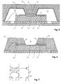
- a first embodiment of the manufacturing process and sensor according to the invention is described by reference to Figs. 1 to 6 .
- This embodiment relates to a sensor that is a temperature sensor as well as a humidity sensor.
- a plurality of sensor chips is manufactured simultaneously on a wafer 1.
- Fig. 1 shows a single chip 5 in detail.
- Each chip may e.g. be a humidity sensor as it is described in US 6 690 569 with a band gap temperature sensor 3 integrated on a first surface 5a thereof.
- Sensitive structure 2 may e.g. be the polymer film of a humidity sensor with underlying electrodes as described in US 6 690 569 .
- further circuitry may be integrated on chip 5, such as analog amplifiers, analog-digital converts and digital processing electronics.
- bond pads 4 are provided on first surface 5a for connecting the band gap circuit and any other circuitry to bond wires.
- Buffer layer 6 is advantageously a photoresist, such as SU-8 by MicroChem Corp., USA. Using a photoresist layer as buffer layer 6 has the advantage that it can be structured easily using standardized processing steps.
- buffer layer 6 is a photoresist, it can be structured directly by means of photolithography in order to remove it at least partially at the location of sensitive structure 2 as well as at the location of the bond pads 4, as shown in Fig. 3 , while leaving it to cover at least band gap circuit 3.
- buffer layer 6 is removed to uncover the contact pads 4 and at least part of sensitive structure 2.
- buffer layer 6 does not cover the contact pads 4 such that the contact pads 4 can later be contacted by the bond wires.
- buffer layer 6 extend over all of sensitive structure 2, but surrounds it, such that said structure can later be exposed to the environment. All steps up to this point can be carried out prior to cutting wafer 1.
- wafer 1 is cut into the chips 5, and a plurality of the chips 5 are placed on a lead frame 7 in known manner, as shown in Fig. 4 .
- the chips 5 may e.g. be glued to the lead frame 7.
- Bond wires 13 are mounted between the contact pads 4 and the leads 7a of lead frame 7.
- lead frame 7 is placed in a mold comprising a lid 8 and a base 9.
- the mold defines an interior space 10 to be filled by a hardening material.
- Lid 8 has a section 11 that extends into interior space 10. Section 11 is located and dimensioned such that, when the mold is closed, it abuts against buffer layer 6 along a circumference of sensitive structure 2, thereby forming a sealed cavity 12 over sensitive structure 2.
- a foil assisted molding process can be used.
- a film 14 is placed over at least one of the parts of mold 8, 9 on the side facing interior space 10.
- Film 14 may e.g. be a ETFE film having a thickness between 50 and 100 ⁇ m.
- a suitable example of such a film is Nowoflon ET6235J by Nowofol, Siegsdorf (Germany) or Fluon by Asahi Glass Co., Japan.
- Such a foil compensates mechanical tolerances, reduces the wear of the mold and simplifies the removal of the mold after the casting process.
- base 9 can be covered by a polyester foil.
- a suitable polyester foil is e.g. RM4100 by Hitachi Chemicals, Japan.
- a hardening material is introduced into the mold to fill interior space 10.
- mold 8 9 is removed, thereby forming the substantially completed device as shown in Fig. 6 .
- section 11 has formed an access opening 15 that connects sensitive structure 2 with the surroundings of the device.
- buffer layer 6 is formed such that it covers bandgap circuit 3 in order to protect it from mechanical stress, such as strain.
- buffer layer 6 advantageously has the following properties:
- buffer layer 6 is advantageously a photoresist, it can also be any other polymer, such as a resin system, e.g. epoxy, in particular a photostructurable resin system such that it can be structured easily. Resin systems have been found to be compatible with the materials that are usually used for injection-molded semiconductor device packaging.
- buffer layer 6 may e.g. also be or comprise a rubber, e.g. silicone rubber, or polyimide. If it is not a photoresist, a separate photoresist layer can e.g. be placed on top of it, which then can be structured to form a mask for subsequently etching the buffer layer at the desired locations.
- a separate photoresist layer can e.g. be placed on top of it, which then can be structured to form a mask for subsequently etching the buffer layer at the desired locations.
- buffer layer 6 may also be applied using printing techniques, such as stencil printing or screen printing, in particular if buffer layer 6 is a silicone rubber.
- buffer layer 6 not only serves to provide a seal with section 11 in the molding process, but it also protects the bandgap circuit 3 from strain. Hence, it is structured such that it covers substantially all of bandgap circuit 3.
- buffer layer 6 can be used not only as a contact surface for section 11 of the mold, but also as a stress relief layer.
- Fig. 7 shows an embodiment of bandgap circuit 3.
- a constant reference voltage can be obtained at output V1, while the voltage difference between outputs V1 and V2 is a measure of the temperature.
- the present invention can also be carried out on temperature sensors without a sensitive structure 2, i.e. on sensors that measure temperature alone.
- the second embodiment shown in Fig. 8 is such a temperature sensor. It differs from the one of Fig. 6 in that all of the first surface 5a of chip 5 is covered by housing 16 and there is no access opening provided therein.
- buffer layer 6 covers substantially all of first surface 5a with the exception of the contact pads 4. At least, it should cover substantially all of bandgap circuit 3.
- the method for manufacturing the second embodiment of Fig. 8 is substantially the same as for manufacturing the first embodiment of Fig. 6 , with the exception that lid 8 has no section 11 extending into interior space 10.
- a temperature sensor with a bandgap circuit 3 is provided.
- Bandgap circuit 3 is covered by a buffer layer 6 of e.g. photoresist.
- Buffer layer 6 is structured and semiconductor chip 5 is packaged in or at least covered by a housing 16.
- mechanical stress as it is e.g. caused by different thermal expansion coefficients of the packaging and the chip, can be reduced.
- the temperature sensor can be an all-solid, monolithic device.
- it advantageously does not comprise a MEMS (a micro electromechanical system), including an IMEMS (an integrated MEMS), as e.g. described in US 6 379 988 .
Landscapes
- Physics & Mathematics (AREA)
- General Physics & Mathematics (AREA)
- Chemical & Material Sciences (AREA)
- Chemical Kinetics & Catalysis (AREA)
- Electrochemistry (AREA)
- Health & Medical Sciences (AREA)
- Life Sciences & Earth Sciences (AREA)
- Analytical Chemistry (AREA)
- Biochemistry (AREA)
- General Health & Medical Sciences (AREA)
- Immunology (AREA)
- Pathology (AREA)
- Structures Or Materials For Encapsulating Or Coating Semiconductor Devices Or Solid State Devices (AREA)
- Encapsulation Of And Coatings For Semiconductor Or Solid State Devices (AREA)
Priority Applications (1)
| Application Number | Priority Date | Filing Date | Title |
|---|---|---|---|
| EP09009135A EP2154714A3 (fr) | 2008-08-11 | 2009-07-14 | Capteur de température avec une couche de détente |
Applications Claiming Priority (2)
| Application Number | Priority Date | Filing Date | Title |
|---|---|---|---|
| EP08014276A EP2154713B1 (fr) | 2008-08-11 | 2008-08-11 | Procédé de fabrication d'un dispositif de capteur avec une couche de détente |
| EP09009135A EP2154714A3 (fr) | 2008-08-11 | 2009-07-14 | Capteur de température avec une couche de détente |
Publications (2)
| Publication Number | Publication Date |
|---|---|
| EP2154714A2 true EP2154714A2 (fr) | 2010-02-17 |
| EP2154714A3 EP2154714A3 (fr) | 2010-03-24 |
Family
ID=40289356
Family Applications (2)
| Application Number | Title | Priority Date | Filing Date |
|---|---|---|---|
| EP08014276A Active EP2154713B1 (fr) | 2008-08-11 | 2008-08-11 | Procédé de fabrication d'un dispositif de capteur avec une couche de détente |
| EP09009135A Withdrawn EP2154714A3 (fr) | 2008-08-11 | 2009-07-14 | Capteur de température avec une couche de détente |
Family Applications Before (1)
| Application Number | Title | Priority Date | Filing Date |
|---|---|---|---|
| EP08014276A Active EP2154713B1 (fr) | 2008-08-11 | 2008-08-11 | Procédé de fabrication d'un dispositif de capteur avec une couche de détente |
Country Status (4)
| Country | Link |
|---|---|
| US (2) | US20100117185A1 (fr) |
| EP (2) | EP2154713B1 (fr) |
| JP (1) | JP5623038B2 (fr) |
| CN (1) | CN101667548A (fr) |
Cited By (1)
| Publication number | Priority date | Publication date | Assignee | Title |
|---|---|---|---|---|
| WO2012100362A1 (fr) * | 2011-01-27 | 2012-08-02 | Sensirion Ag | Procédé pour fabriquer une puce de capteur |
Families Citing this family (43)
| Publication number | Priority date | Publication date | Assignee | Title |
|---|---|---|---|---|
| EP2154713B1 (fr) | 2008-08-11 | 2013-01-02 | Sensirion AG | Procédé de fabrication d'un dispositif de capteur avec une couche de détente |
| EP2224218B1 (fr) * | 2009-02-25 | 2018-11-28 | Sensirion Automotive Solutions AG | Capteur dans un emballage moulé et son procédé de fabrication |
| WO2010113712A1 (fr) * | 2009-03-31 | 2010-10-07 | アルプス電気株式会社 | Capteur d'humidité de type capacitif et son procédé de production |
| DE102010033963A1 (de) * | 2010-08-11 | 2012-02-16 | Osram Opto Semiconductors Gmbh | Optoelektronisches Bauelement und Verfahren zur Herstellung eines optoelektronischen Bauelements |
| DE102011004381A1 (de) * | 2011-02-18 | 2012-08-23 | Robert Bosch Gmbh | Moldmodul mit Sensorelement |
| DE102011013468A1 (de) * | 2011-03-09 | 2012-09-13 | Micronas Gmbh | Halbleitergehäuse und Verfahren zur Herstellung eines Halbleitergehäuses |
| EP2573804A1 (fr) * | 2011-09-21 | 2013-03-27 | Nxp B.V. | Circuit intégré avec capteur et procédé de sa fabrication |
| JP5708688B2 (ja) * | 2012-08-27 | 2015-04-30 | 株式会社デンソー | センサパッケージの製造方法 |
| JP6018903B2 (ja) | 2012-12-17 | 2016-11-02 | 日立オートモティブシステムズ株式会社 | 物理量センサ |
| DE102013217888B4 (de) | 2012-12-20 | 2024-07-04 | Continental Automotive Technologies GmbH | Elektronische Vorrichtung und Verfahren zur Herstellung einer elektronischen Vorrichtung |
| DE102012224424A1 (de) * | 2012-12-27 | 2014-07-17 | Robert Bosch Gmbh | Sensorsystem und Abdeckvorrichtung für ein Sensorsystem |
| JP6068684B2 (ja) | 2013-02-28 | 2017-01-25 | ヒューレット−パッカード デベロップメント カンパニー エル.ピー.Hewlett‐Packard Development Company, L.P. | 流体流れ構造の成形 |
| US10821729B2 (en) | 2013-02-28 | 2020-11-03 | Hewlett-Packard Development Company, L.P. | Transfer molded fluid flow structure |
| KR102005466B1 (ko) | 2013-02-28 | 2019-07-30 | 휴렛-팩커드 디벨롭먼트 컴퍼니, 엘.피. | 프린트 바 |
| US9724920B2 (en) | 2013-03-20 | 2017-08-08 | Hewlett-Packard Development Company, L.P. | Molded die slivers with exposed front and back surfaces |
| EP2871152B1 (fr) | 2013-11-06 | 2017-05-24 | Sensirion AG | Dispositif capteur |
| KR20150074427A (ko) * | 2013-12-24 | 2015-07-02 | 삼성전기주식회사 | 센서 패키지 및 이를 구비하는 휴대 단말기 |
| CN108615711A (zh) * | 2014-01-24 | 2018-10-02 | 清华大学 | 一种基于模板的封装结构及封装方法 |
| EP2942807B1 (fr) * | 2014-05-07 | 2020-08-26 | Sensirion AG | Conditionnement de semi-conducteur |
| EP3001186B1 (fr) | 2014-09-26 | 2018-06-06 | Sensirion AG | Puce de capteur |
| EP3032227B1 (fr) | 2014-12-08 | 2020-10-21 | Sensirion AG | Package de capteur de débit |
| US9355870B1 (en) | 2015-01-15 | 2016-05-31 | Silicon Laboratories Inc. | Integrated circuit with sensor area and resin dam |
| US20160360622A1 (en) * | 2015-06-02 | 2016-12-08 | Microchip Technology Incorporated | Integrated Circuit With Sensor Printed In Situ |
| EP3168866B1 (fr) | 2015-11-16 | 2020-12-30 | ams AG | Dispositif capteur d'humidité à semi-conducteur et son procédé de fabrication |
| US9781324B2 (en) * | 2016-02-18 | 2017-10-03 | Ningbo Sunny Opotech Co., Ltd. | Array imaging module and molded photosensitive assembly, circuit board assembly and manufacturing methods thereof for electronic device |
| US20190148429A1 (en) * | 2016-03-12 | 2019-05-16 | Ningbo Sunny Opotech Co., Ltd. | Camera module, and photosensitive component thereof and manufacturing method therefor |
| EP3429181B1 (fr) * | 2016-03-12 | 2024-10-16 | Ningbo Sunny Opotech Co., Ltd. | Module de caméra de réseau, ensemble photosensible moulé, son procédé de fabrication et dispositif électronique |
| US9899290B2 (en) * | 2016-03-23 | 2018-02-20 | Nxp Usa, Inc. | Methods for manufacturing a packaged device with an extended structure for forming an opening in the encapsulant |
| US9799580B2 (en) | 2016-03-24 | 2017-10-24 | Nxp Usa, Inc. | Semiconductor device package and methods of manufacture thereof |
| EP3468165B1 (fr) * | 2016-03-28 | 2023-12-20 | Ningbo Sunny Opotech Co., Ltd. | Module de caméra et ensemble photosensible moulé et son procédé de fabrication, et dispositif électronique |
| CN105681640B (zh) * | 2016-03-28 | 2019-12-27 | 宁波舜宇光电信息有限公司 | 摄像模组及其制造方法 |
| US10659664B2 (en) * | 2016-08-01 | 2020-05-19 | Ningbo Sunny Opotech Co., Ltd. | Camera module and molded circuit board assembly and manufacturing method thereof |
| CN109716745B (zh) * | 2016-08-01 | 2020-12-18 | 宁波舜宇光电信息有限公司 | 摄像模组及其模塑电路板组件和模塑感光组件和制造方法 |
| TWI698125B (zh) * | 2016-08-01 | 2020-07-01 | 大陸商寧波舜宇光電信息有限公司 | 攝像模組及其模塑感光元件和製造方法 |
| WO2018184572A1 (fr) | 2017-04-07 | 2018-10-11 | 宁波舜宇光电信息有限公司 | Procédé d'encapsulation de semi-conducteur à base de technique de moulage et dispositif à semi-conducteur |
| CN207664026U (zh) * | 2017-04-07 | 2018-07-27 | 宁波舜宇光电信息有限公司 | 基于模制工艺的半导体装置及包含该半导体装置的图像处理组件、摄像装置和电子设备 |
| JP6780675B2 (ja) | 2017-07-24 | 2020-11-04 | 株式会社デンソー | 半導体装置及び半導体装置の製造方法 |
| CN109524372A (zh) * | 2018-12-29 | 2019-03-26 | 山东盛品电子技术有限公司 | 封装结构、解决传感器芯片封装后封装体内部应力的方法 |
| WO2021004470A1 (fr) * | 2019-07-10 | 2021-01-14 | 宁波舜宇光电信息有限公司 | Procédé de préparation d'un ensemble photosensible, ensemble photosensible et module de photographie |
| JP7442333B2 (ja) * | 2020-02-12 | 2024-03-04 | エイブリック株式会社 | 半導体装置およびその製造方法 |
| US11804416B2 (en) | 2020-09-08 | 2023-10-31 | UTAC Headquarters Pte. Ltd. | Semiconductor device and method of forming protective layer around cavity of semiconductor die |
| JPWO2024214655A1 (fr) * | 2023-04-12 | 2024-10-17 | ||
| IT202300024078A1 (it) * | 2023-11-14 | 2025-05-14 | St Microelectronics Int Nv | Procedimento per fabbricare generatori termoelettrici |
Citations (2)
| Publication number | Priority date | Publication date | Assignee | Title |
|---|---|---|---|---|
| US6379988B1 (en) | 2000-05-16 | 2002-04-30 | Sandia Corporation | Pre-release plastic packaging of MEMS and IMEMS devices |
| US6690569B1 (en) | 1999-12-08 | 2004-02-10 | Sensirion A/G | Capacitive sensor |
Family Cites Families (45)
| Publication number | Priority date | Publication date | Assignee | Title |
|---|---|---|---|---|
| US2154713A (en) * | 1936-04-17 | 1939-04-18 | Shell Dev | Process for extracting ethereal oils |
| US4620502A (en) * | 1986-01-31 | 1986-11-04 | Kimble Erma N | Hand sanitizer |
| JPS62254451A (ja) * | 1986-04-28 | 1987-11-06 | Canon Inc | 電子部品装置 |
| JPH0724287B2 (ja) * | 1987-02-12 | 1995-03-15 | 三菱電機株式会社 | 光透過用窓を有する半導体装置とその製造方法 |
| US4888988A (en) * | 1987-12-23 | 1989-12-26 | Siemens-Bendix Automotive Electronics L.P. | Silicon based mass airflow sensor and its fabrication method |
| US5026667A (en) * | 1987-12-29 | 1991-06-25 | Analog Devices, Incorporated | Producing integrated circuit chips with reduced stress effects |
| JPH02227485A (ja) | 1989-02-28 | 1990-09-10 | Mitsubishi Electric Corp | 半導体封止材料 |
| SE469415B (sv) * | 1991-11-21 | 1993-07-05 | Rollen Jarl Erik | Foerfarande och medel foer att aastadkomma och uppraetthaalla en mikrobiologiskt ren rumsmiljoe |
| US5332469A (en) * | 1992-11-12 | 1994-07-26 | Ford Motor Company | Capacitive surface micromachined differential pressure sensor |
| NL9400766A (nl) * | 1994-05-09 | 1995-12-01 | Euratec Bv | Werkwijze voor het inkapselen van een geintegreerde halfgeleiderschakeling. |
| NL1003315C2 (nl) * | 1996-06-11 | 1997-12-17 | Europ Semiconductor Assembly E | Werkwijze voor het inkapselen van een geïntegreerde halfgeleiderschake- ling. |
| CN1270628A (zh) * | 1997-07-31 | 2000-10-18 | 普罗克特和甘保尔公司 | 湿状清洁制品 |
| US6313049B1 (en) * | 1998-05-04 | 2001-11-06 | Dotty Heady | Disposable fabric-saturated sanitizer wipe(s) for food industry with sealed container packaging therefor |
| NL1011929C2 (nl) * | 1999-04-29 | 2000-10-31 | 3P Licensing Bv | Werkwijze voor het inkapselen van elektronische componenten, in het bijzonder geintegreerde schakelingen. |
| DE19929025A1 (de) | 1999-06-25 | 2000-12-28 | Bosch Gmbh Robert | Drucksensor |
| EP1236037B1 (fr) * | 1999-11-30 | 2007-10-10 | Sensirion AG | Capteur place dans un boitier |
| US6489178B2 (en) * | 2000-01-26 | 2002-12-03 | Texas Instruments Incorporated | Method of fabricating a molded package for micromechanical devices |
| AT410727B (de) * | 2000-03-14 | 2003-07-25 | Austria Mikrosysteme Int | Verfahren zum unterbringen von sensoren in einem gehäuse |
| CH695166A5 (de) * | 2000-04-25 | 2005-12-30 | Sensirion Ag | Verfahren und Vorrichtung zum Messen des Flusses einer Flüssigkeit. |
| US6794352B2 (en) * | 2000-06-12 | 2004-09-21 | Jeffrey S. Svendsen | Cleaning towel having a color identifying label and sanitizer release polymer composition |
| US6729181B2 (en) * | 2000-08-23 | 2004-05-04 | Sensiron Ag | Flow sensor in a housing |
| NL1018403C1 (nl) | 2000-10-05 | 2002-04-08 | Boschman Tech Bv | Werkwijze voor het onder toepassing van een laser snijden van een composietstructuur met een of meer elektronische componenten. |
| EP1211722B9 (fr) | 2000-11-30 | 2005-07-13 | STMicroelectronics S.r.l. | Procédé de fabrication d'un empaquetage pour dispositif électronique |
| EP1220309A1 (fr) * | 2000-12-28 | 2002-07-03 | STMicroelectronics S.r.l. | Procédé de fabrication d'un empaquetage pour dispositif électronique |
| US7154372B2 (en) * | 2001-01-10 | 2006-12-26 | Sensirion Ag | Micromechanical flow sensor with tensile coating |
| EP1246235A1 (fr) * | 2001-03-26 | 2002-10-02 | European Semiconductor Assembly (Eurasem) B.V. | Procédé d'encapsulation d'une puce ayant une surface sensible |
| NL1019042C2 (nl) * | 2001-09-26 | 2003-03-27 | Europ Semiconductor Assembly E | Werkwijze voor het inkapselen van een chip en/of ander voorwerp. |
| JP3882592B2 (ja) * | 2001-11-26 | 2007-02-21 | 松下電工株式会社 | 半導体イオンセンサとその製造方法 |
| US20030191692A1 (en) * | 2002-04-05 | 2003-10-09 | Vogel Philip S. | Method for a restaurant to do business including the step of providing hand sanitizer to customers |
| US7109574B2 (en) * | 2002-07-26 | 2006-09-19 | Stmicroelectronics, Inc. | Integrated circuit package with exposed die surfaces and auxiliary attachment |
| GB0307616D0 (en) * | 2003-04-02 | 2003-05-07 | Melexis Nv | Calorimetric flow meter |
| TW200522292A (en) * | 2003-12-31 | 2005-07-01 | Advanced Semiconductor Eng | Chip package sturcture |
| JP2004266844A (ja) * | 2004-03-26 | 2004-09-24 | Mitsubishi Electric Corp | 撮像装置及びその製造方法 |
| EP1628132B1 (fr) * | 2004-08-17 | 2015-01-07 | Sensirion Holding AG | Procédé et appareil de calibrage de capteurs |
| US20060153733A1 (en) * | 2005-01-10 | 2006-07-13 | Simon Sassoon | Door handle sanitizer system and apparatus |
| US7067350B1 (en) * | 2005-01-31 | 2006-06-27 | Taiwan Semiconductor Manufacturing Company, Ltd. | Method of manufacturing a semiconductor device using electrical contacts formed in an isolation layer |
| WO2006114005A1 (fr) | 2005-04-27 | 2006-11-02 | Sensirion Ag | Procede d'encapsulation de capteurs integres |
| US20060289558A1 (en) * | 2005-06-28 | 2006-12-28 | Parker Kimberly A | Publicly-accessible moist hand cleaning wipe station |
| DE102005047856B4 (de) * | 2005-10-05 | 2007-09-06 | Infineon Technologies Ag | Halbleiterbauteil mit in Kunststoffgehäusemasse eingebetteten Halbleiterbauteilkomponenten, Systemträger zur Aufnahme der Halbleiterbauteilkomponenten und Verfahren zur Herstellung des Systemträgers und von Halbleiterbauteilen |
| EP1873499A1 (fr) | 2006-06-30 | 2008-01-02 | Sensirion AG | Capteur thermique de débit pour écoulement à grande vitesse |
| DE112006004083T5 (de) * | 2006-10-18 | 2009-11-26 | Sensirion Holding Ag | Verfahren zum Verpacken integrierter Sensoren |
| US20080193495A1 (en) * | 2007-02-14 | 2008-08-14 | Maryam Yousefi Kharazmi | Disposable hand sanitizer gel dispenser |
| US20080258318A1 (en) * | 2007-04-20 | 2008-10-23 | Nec Electronics Corporation | Semiconductor device |
| JP2009081346A (ja) * | 2007-09-27 | 2009-04-16 | Panasonic Corp | 光学デバイスおよびその製造方法 |
| EP2154713B1 (fr) * | 2008-08-11 | 2013-01-02 | Sensirion AG | Procédé de fabrication d'un dispositif de capteur avec une couche de détente |
-
2008
- 2008-08-11 EP EP08014276A patent/EP2154713B1/fr active Active
-
2009
- 2009-07-14 EP EP09009135A patent/EP2154714A3/fr not_active Withdrawn
- 2009-07-14 US US12/460,152 patent/US20100117185A1/en not_active Abandoned
- 2009-08-05 US US12/462,528 patent/US7901971B2/en active Active
- 2009-08-10 JP JP2009185388A patent/JP5623038B2/ja active Active
- 2009-08-11 CN CN200910173376A patent/CN101667548A/zh active Pending
Patent Citations (2)
| Publication number | Priority date | Publication date | Assignee | Title |
|---|---|---|---|---|
| US6690569B1 (en) | 1999-12-08 | 2004-02-10 | Sensirion A/G | Capacitive sensor |
| US6379988B1 (en) | 2000-05-16 | 2002-04-30 | Sandia Corporation | Pre-release plastic packaging of MEMS and IMEMS devices |
Cited By (1)
| Publication number | Priority date | Publication date | Assignee | Title |
|---|---|---|---|---|
| WO2012100362A1 (fr) * | 2011-01-27 | 2012-08-02 | Sensirion Ag | Procédé pour fabriquer une puce de capteur |
Also Published As
| Publication number | Publication date |
|---|---|
| JP2010050452A (ja) | 2010-03-04 |
| EP2154713B1 (fr) | 2013-01-02 |
| US20100035373A1 (en) | 2010-02-11 |
| JP5623038B2 (ja) | 2014-11-12 |
| EP2154713A1 (fr) | 2010-02-17 |
| CN101667548A (zh) | 2010-03-10 |
| US20100117185A1 (en) | 2010-05-13 |
| EP2154714A3 (fr) | 2010-03-24 |
| US7901971B2 (en) | 2011-03-08 |
Similar Documents
| Publication | Publication Date | Title |
|---|---|---|
| EP2154714A2 (fr) | Capteur de température avec une couche de détente | |
| US7880244B2 (en) | Wafer level CSP sensor | |
| US11192777B2 (en) | MEMS sensor package systems and methods | |
| US9105649B2 (en) | Semiconductor component and corresponding production method | |
| US9731959B2 (en) | Integrated device packages having a MEMS die sealed in a cavity by a processor die and method of manufacturing the same | |
| US9885626B2 (en) | Micromechanical sensor system and corresponding manufacturing method | |
| WO2012100362A1 (fr) | Procédé pour fabriquer une puce de capteur | |
| WO2011062242A1 (fr) | Dispositif de détection et son procédé de fabrication | |
| CN106082110B (zh) | 芯片封装体及其制造方法 | |
| EP3601957B1 (fr) | Boîtier de capteur | |
| US10858245B2 (en) | Deposition of protective material at wafer level in front end for early stage particle and moisture protection | |
| CN105470212A (zh) | 用于半导体器件的封装及其组装方法 | |
| US12024418B2 (en) | Method of manufacturing a sensor device and moulding support structure | |
| US7617599B2 (en) | Sensor packaging method for a human contact interface | |
| JP4675945B2 (ja) | 半導体装置 | |
| Shaw et al. | Package design of pressure sensors for high volume consumer applications | |
| US11823968B2 (en) | Semiconductor device package having stress isolation and method therefor | |
| CN119706727A (zh) | 集成传感器装置 |
Legal Events
| Date | Code | Title | Description |
|---|---|---|---|
| PUAI | Public reference made under article 153(3) epc to a published international application that has entered the european phase |
Free format text: ORIGINAL CODE: 0009012 |
|
| AK | Designated contracting states |
Kind code of ref document: A2 Designated state(s): AT BE BG CH CY CZ DE DK EE ES FI FR GB GR HR HU IE IS IT LI LT LU LV MC MK MT NL NO PL PT RO SE SI SK SM TR |
|
| AX | Request for extension of the european patent |
Extension state: AL BA RS |
|
| PUAL | Search report despatched |
Free format text: ORIGINAL CODE: 0009013 |
|
| AK | Designated contracting states |
Kind code of ref document: A3 Designated state(s): AT BE BG CH CY CZ DE DK EE ES FI FR GB GR HR HU IE IS IT LI LT LU LV MC MK MT NL NO PL PT RO SE SI SK SM TR |
|
| AX | Request for extension of the european patent |
Extension state: AL BA RS |
|
| STAA | Information on the status of an ep patent application or granted ep patent |
Free format text: STATUS: THE APPLICATION IS DEEMED TO BE WITHDRAWN |
|
| 18D | Application deemed to be withdrawn |
Effective date: 20100925 |