EP2154717A2 - Materialien zur Klebverbesserung einer Kupferfolie auf Diffusionsabgrenzungen - Google Patents
Materialien zur Klebverbesserung einer Kupferfolie auf Diffusionsabgrenzungen Download PDFInfo
- Publication number
- EP2154717A2 EP2154717A2 EP09167949A EP09167949A EP2154717A2 EP 2154717 A2 EP2154717 A2 EP 2154717A2 EP 09167949 A EP09167949 A EP 09167949A EP 09167949 A EP09167949 A EP 09167949A EP 2154717 A2 EP2154717 A2 EP 2154717A2
- Authority
- EP
- European Patent Office
- Prior art keywords
- carbon atoms
- layer
- groups
- chromium
- group
- Prior art date
- Legal status (The legal status is an assumption and is not a legal conclusion. Google has not performed a legal analysis and makes no representation as to the accuracy of the status listed.)
- Withdrawn
Links
Images





Classifications
-
- H—ELECTRICITY
- H10—SEMICONDUCTOR DEVICES; ELECTRIC SOLID-STATE DEVICES NOT OTHERWISE PROVIDED FOR
- H10D—INORGANIC ELECTRIC SEMICONDUCTOR DEVICES
- H10D64/00—Electrodes of devices having potential barriers
- H10D64/01—Manufacture or treatment
- H10D64/011—Manufacture or treatment of electrodes ohmically coupled to a semiconductor
-
- H—ELECTRICITY
- H10—SEMICONDUCTOR DEVICES; ELECTRIC SOLID-STATE DEVICES NOT OTHERWISE PROVIDED FOR
- H10W—GENERIC PACKAGES, INTERCONNECTIONS, CONNECTORS OR OTHER CONSTRUCTIONAL DETAILS OF DEVICES COVERED BY CLASS H10
- H10W20/00—Interconnections in chips, wafers or substrates
- H10W20/01—Manufacture or treatment
- H10W20/031—Manufacture or treatment of conductive parts of the interconnections
- H10W20/032—Manufacture or treatment of conductive parts of the interconnections of conductive barrier, adhesion or liner layers
- H10W20/033—Manufacture or treatment of conductive parts of the interconnections of conductive barrier, adhesion or liner layers in openings in dielectrics
- H10W20/035—Manufacture or treatment of conductive parts of the interconnections of conductive barrier, adhesion or liner layers in openings in dielectrics combinations of barrier, adhesion or liner layers, e.g. multi-layered barrier layers
-
- C—CHEMISTRY; METALLURGY
- C22—METALLURGY; FERROUS OR NON-FERROUS ALLOYS; TREATMENT OF ALLOYS OR NON-FERROUS METALS
- C22C—ALLOYS
- C22C1/00—Making non-ferrous alloys
Definitions
- US 6271131 discloses a method of forming a rhodium (Rh) containing layer such as platinum-rhodium (Pt-Rh) alloy as diffusion barrier via chemical vapor deposition.
- Rh rhodium
- Pt-Rh platinum-rhodium
- Ti-Ta titanium-tantalum
- the Ti rich/Ta deficient portion provides good adhesion to the dielectric film and the Ta rich/Ti deficient portion forms a hetero-epitaxial interface with the interconnect film and suppresses the formation of intermetallic compounds.
- US 5942799 discloses a multilayer diffusion barrier comprising a refractory metal such as tungsten (W), titanium (Ti), tantalum (Ta), molybdenum (Mo); and a refractory metal nitride such as WN x , TiN, TaN; and a second sublayer formed from a refractory metal nitride, a refractory metal silicon nitride such as TiSi x N y , TaSi x N y , WSi x N y .
- a refractory metal such as tungsten (W), titanium (Ti), tantalum (Ta), molybdenum (Mo)
- a refractory metal nitride such as WN x , TiN, TaN
- a second sublayer formed from a refractory metal nitride, a refractory metal silicon nitride such as TiSi x N y
- US 20050070097 discloses a very thin multilayer diffusion barrier for a semiconductor device and fabrication method thereof.
- the multilayer diffusion barrier is fabricated by forming a very thin, multilayer diffusion barrier composed of even thinner sub-layers, where the sub-layers are only a few atoms thick.
- US 2006001306 reveals a method to enhance thermal stability and reliability by forming a hybrid type nanocomposite diffusion barrier deposited by atomic layer deposition using precursors composing of a Ti precursor and a Ta precursor.
- WO 2006115476 covers the ruthenium alloy as copper diffusion barrier comprising of ruthenium and at least one element from groups IV, V, or VI of the Periodic Table or a combination thereof.
- US 20070264816 discloses a method for forming a metal interconnect to use a Cu-Al alloy layer on the barrier layer.
- the Cu--Al alloy layer may be formed by sequential ALD or CVD deposition of an aluminum layer and a copper layer followed by an annealing process. Alternately, the Cu--Al alloy layer may be formed in-situ by co-pulsing the aluminum and copper precursors.
- US 20070123043 describes a tin and nickel-containing copper alloy as diffusion barrier in a copper interconnect.
- the tin and nickel-containing copper alloy may be formed in a gaseous ambient on the basis of tin hydride and nickel, carbon monoxide in a thermally driven reaction.
- the state-of-the-art computational chemistry techniques have been used to identify adhesion promoting layer materials that provide good adhesion of metal seed layer to the adhesion promoting layer and the adhesion promoting layer to the barrier layer.
- Methods of controlling agglomeration and improving adhesion, a semiconductor device structure having controlled agglomeration and improving adhesion, and a chromium precursor for making chromium alloys as the adhesion promoting layer material have also been disclosed.
- a method comprising:
- the method according to the first or second aspect is for producing a semiconductor device.
- On advantage of such methods is that agglomeration of atoms in a metal seed layer of the semiconductor device is controlled and adhesion between the metal seed layer and a diffusion barrier layer is improved.
- the method according to the first or second aspect is preferably for controlling agglomeration and improving adhesion of a semiconductor device.
- a semiconductor device structure comprises:
- a chromium containing complex of a polydentate ⁇ -ketoiminate is selected from the group consisting of structure A , and structure B; wherein:
- a chromium alloy to control agglomeration in a conductive metal seed layer provided on a barrier layer in a semiconductor device and/or improve adherence of said metal seed layer to said barrier layer.
- Copper adhesion to barrier layers and electromigration resistance are extremely important properties affecting device yield and device lifetimes.
- the state-of-the-art computational chemistry techniques have been used to identify adhesion promoting layer materials that provide good adhesion of metal seed layer to the adhesion promoting layer and the adhesion promoting layer to the barrier layer.
- adhesion promoting layer or a "glue” layer, is applied directly to a barrier layer to improve the adhesion of the subsequently deposited metal seed layer.
- Suitable barrier layers comprise a material selected from the group consisting of: tantalum (Ta), tantalum-nitride (TaN), tantalum-silicon-nitride (TaSiN), titanium (Ti), titanium-nitride (TiN), and mixtures thereof.
- Suitable metal seed layer is selected from a copper layer, a copper alloy layer, and combinations thereof.
- Suitable chromium alloys including chromium and about 10 % to about 90% atomic weight percentage of an alloying element.
- the chromium alloys include chromium-copper (Cr x Cu y ), chromium-silver (Cr x Ag y ), chromium-ruthenium (Cr x Ru y ), chromium-vanadium (Cr x V y ), chromium-tantalum (Cr x Ta y ), chromium-titanium (Cr x Ti y ), chromium-zirconium (Cr x Zr y ) and chromium-niobium (Cr x Nb y ); where x is in the range of 10% to 90%.
- the adhesion promoting layer may be deposited by a process selected from the group consisting of Atomic Layer Deposition (ALD), Plasma Enhanced Atomic Layer Deposition (PEALD), Chemical Vapor Deposition(CVD), and Plasma Enhanced Chemical Vapor Deposition(PECVD), Low Pressure Chemical Vapor Deposition(LPCVD), Sub Atmospheric Chemical Vapor Deposition(SACVD), UV assisted Chemical Vapor Deposition, Filament assisted Chemical Vapor Deposition (FACVD), and Atmospheric Pressure Chemical Vapor Deposition (APCVD ).
- ALD Atomic Layer Deposition
- PEALD Plasma Enhanced Atomic Layer Deposition
- CVD Chemical Vapor Deposition
- PECVD Plasma Enhanced Chemical Vapor Deposition
- LPCVD Low Pressure Chemical Vapor Deposition
- SACVD Sub Atmospheric Chemical Vapor Deposition
- FACVD Filament assisted Chemical Vapor Deposition
- APCVD Atmospheric Pressure Chemical Vapor Deposition
- Suitable chromium containing precursors for depositing the chromium alloys are chromium containing complexes of a polydentate ⁇ -ketoiminate represented by the following structures A and B: wherein:
- the TaN(111) surface is described with a slab model containing four alternating layers with Ta (tantalum) and N (nitrogen) with N on top ( Figure 1 ).
- Density functional theory (DFT) calculations under the generalized gradient approximation were performed using the exchange-correlation functional proposed by Perdew-Wang ( Perdew, J. P. and Wang, Y.; Phys. Rev. B; 1992, 45, 13244 ).
- the projector augmented wave (“PAW”) pseudopotentials are used to represent the core electrons, while the valence orbitals are described by a plane wave basis set with 400 electon volts (“eV”) energy cut-off, which is sufficient to produce well-converged results.
- the electronically open-shell system was treated with a spin polarization scheme.
- the Brillouin zone integration was performed using the Monkhorst and Pack scheme ( Monkhorst, H. J. and Pack, J.
- the inventors subsequently performed ab initio molecular dynamics ("MD") simulations for duration of 3.5 picoseconds (“ps”) with a time step of 1 femtosecond (“fs”) at 500 K to study the dynamic behavior of a Cu monolayer on the barrier surface in a canonical ensemble using the Nose thermostat for temperature control. All calculations were carried out using the VASP, or the Vienna Ab-initio simulation package.
- MD ab initio molecular dynamics
- Figure 2 displays several selected snapshots of the MD trajectory.
- the Cu monolayer is well aligned and commensurate with the substrate.
- Cu atoms are then quickly disassembled and move away from their equilibrium positions through surface diffusion upon MD run.
- Further MD runs prompt Cu atoms to move continuously, forming surface islands of various shapes, but no wetting of copper clusters on the surface was observed.
- the calculated adhesion energy of Cu monolayer on TaN(111) is 2.65 eV.
- Ru (Ruthenium) as an adhesion promoting material
- Figure 3(a) displays a fully equilibrated structure upon 4 ps MD simulation. No agglomeration of Cu atoms, other than simple thermal motion, was observed. Placing the same monolayer on several layers of Ru, as shown in Fig. 3(b) , results in no agglomeration of Cu atoms.
- the calculated adhesion energy of Cu monolayer on the Ru monolayer is 3.50 eV and the calculated adhesion energy of Ru monolayer on TaN(111) is 5.01 eV, significantly larger than the adhesion energy of Cu monolayer on TaN(111).
- the results suggest that Cu monolayer will not agglomerate on the Ru adhesion promoting layer.
- Ta Ta (Tantalum) as an adhesion promoting material
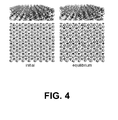
- Figure 4 displays a fully equilibrated structure upon 4 ps MD simulation. No agglomeration of Cu atoms, other than simple thermal motion, was observed. Placing the same monolayer on multi-layers of Ta results in no agglomeration of Cu atoms.
- the calculated adhesion energy of Cu monolayer on the Ta monolayer is 3.84 eV and the calculated adhesion energy of Ta monolayer on TaN(111) is 7.72 eV, significantly larger than the adhesion energy of Cu monolayer on TaN(111).
- the results suggest that Cu monolayer will not agglomerate on the Ta adhesion promoting layer.
- Figure 5 displays a fully equilibrated structure upon 4 ps MD simulation. No agglomeration of Cu atoms, other than simple thermal motion, was observed. Placing the same monolayer on multi-layers of Cr results in no agglomeration of Cu atoms.
- the calculated adhesion energy of Cu monolayer on the Cr monolayer is 3.52 eV and the calculated adhesion energy of Ta monolayer on TaN(111) is 5.10 eV, significantly larger than the adhesion energy of Cu monolayer on TaN(111). The results suggest that Cu monolayer will not agglomerate on the Cr adhesion promoting layer.
- Figure 6 displays equilibrated structures upon 4 ps MD simulation.
- Figure 6(a) displays a fully equilibrium structure of CrV adhesion promoting layer on TaN(111) surface with top view and side view.
- Figure 6(b) displays a fully equilibrium structure of Cu monolayer on the CrV adhesion promoting layer on TaN(111) surface with top view and side view.
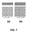
- Figure 7 displays equilibrated structures upon 4 ps MD simulation.
- Figure 7(a) displays the equilibrium structure of CrTi adhesion promoting layer on TaN(111) surface with top view and side view.
- Figure 7(b) displays the equilibrium structure of Cu monolayer on the CrTi adhesion promoting layer on TaN(111) surface with top view and side view.
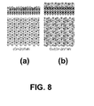
- Figure 8 displays equilibrated structures upon 4 ps MD simulation.
- Figure 8(a) displays the equilibrium structure of CrZr adhesion promoting layer on TaN(111) surface with top view and side view.
- Figure 8(b) displays the equilibrium structure of Cu monolayer on the CrZr adhesion promoting layer on TaN(111) surface with top view and side view.
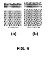
- Figure 9 displays equilibrated structures upon 4 ps MD simulation.
- Figure 9(a) displays the equilibrium structure of CrNb adhesion promoting layer on TaN(111) surface with top view and side view.
- Figure 9(b) displays the equilibrium structure of Cu monolayer on the CrNb adhesion promoting layer on TaN(111) surface with top view and side view.
- the inventors have identified factors responsible for providing good adhesion of copper layer on various metallic surfaces and circumstances under which agglomeration of copper film occur.
- the adhesion energy of the adhesion promoting layer on the barrier layer should be higher than the adhesion energy of copper on the barrier layer.
- the adhesion energy of the copper seed layer on the adhesion promoting layer should be higher than the adhesion energy of copper on the barrier layer (otherwise, the copper seed layer would agglomerate on the glue layer);
- the adhesion energy of adhesion promoting layer on the barrier layer should be higher than the adhesion energy of the copper seed layer on the glue layer.
- Chromium containing complexes of a polydentate ⁇ -ketoiminate have been identified as chromium containing precursors to make the chromium alloys used for the adhesion promoting layer.
Landscapes
- Chemical & Material Sciences (AREA)
- Engineering & Computer Science (AREA)
- Materials Engineering (AREA)
- Mechanical Engineering (AREA)
- Metallurgy (AREA)
- Organic Chemistry (AREA)
- Internal Circuitry In Semiconductor Integrated Circuit Devices (AREA)
- Electrodes Of Semiconductors (AREA)
- Chemical Vapour Deposition (AREA)
- Laminated Bodies (AREA)
Applications Claiming Priority (1)
| Application Number | Priority Date | Filing Date | Title |
|---|---|---|---|
| US12/192,603 US7919409B2 (en) | 2008-08-15 | 2008-08-15 | Materials for adhesion enhancement of copper film on diffusion barriers |
Publications (1)
| Publication Number | Publication Date |
|---|---|
| EP2154717A2 true EP2154717A2 (de) | 2010-02-17 |
Family
ID=41319973
Family Applications (1)
| Application Number | Title | Priority Date | Filing Date |
|---|---|---|---|
| EP09167949A Withdrawn EP2154717A2 (de) | 2008-08-15 | 2009-08-14 | Materialien zur Klebverbesserung einer Kupferfolie auf Diffusionsabgrenzungen |
Country Status (6)
| Country | Link |
|---|---|
| US (1) | US7919409B2 (de) |
| EP (1) | EP2154717A2 (de) |
| JP (1) | JP2010062555A (de) |
| KR (1) | KR20100021379A (de) |
| CN (1) | CN101673706A (de) |
| TW (1) | TW201007844A (de) |
Cited By (1)
| Publication number | Priority date | Publication date | Assignee | Title |
|---|---|---|---|---|
| US20140377948A1 (en) * | 2006-12-19 | 2014-12-25 | Spansion Llc | Method of depositing copper using physical vapor deposition |
Families Citing this family (4)
| Publication number | Priority date | Publication date | Assignee | Title |
|---|---|---|---|---|
| US20090237209A1 (en) * | 2008-03-20 | 2009-09-24 | Brian William Seal | Communicating keychain |
| KR100973277B1 (ko) * | 2008-08-29 | 2010-07-30 | 주식회사 하이닉스반도체 | 반도체 소자의 금속배선 및 그 형성방법 |
| EP3876307B1 (de) * | 2018-11-09 | 2024-07-10 | Shenzhen Yuanzi Technology Co., Ltd. | Folienherstellungsverfahren |
| WO2025183176A1 (ja) * | 2024-02-29 | 2025-09-04 | 公立大学法人大阪 | 強誘電体デバイスおよびその製造方法 |
Citations (8)
| Publication number | Priority date | Publication date | Assignee | Title |
|---|---|---|---|---|
| US5942799A (en) | 1997-11-20 | 1999-08-24 | Novellus Systems, Inc. | Multilayer diffusion barriers |
| US6271131B1 (en) | 1998-08-26 | 2001-08-07 | Micron Technology, Inc. | Methods for forming rhodium-containing layers such as platinum-rhodium barrier layers |
| US6331484B1 (en) | 1999-03-29 | 2001-12-18 | Lucent Technologies, Inc. | Titanium-tantalum barrier layer film and method for forming the same |
| US20050070097A1 (en) | 2003-09-29 | 2005-03-31 | International Business Machines Corporation | Atomic laminates for diffusion barrier applications |
| US20060001306A1 (en) | 2004-07-02 | 2006-01-05 | C. Rob. Hammerstein Gmbh & Co. Kg | Automotive vehicle seat with a lengthwise adjustment device, a seat carrier and rear rockers |
| WO2006115476A2 (en) | 2005-04-21 | 2006-11-02 | Honeywell International Inc. | Ruthenium-based materials and ruthenium alloys |
| US20070123043A1 (en) | 2005-11-30 | 2007-05-31 | Christof Streck | A semiconductor device comprising a copper alloy as a barrier layer in a copper metallization layer |
| US20070264816A1 (en) | 2006-05-12 | 2007-11-15 | Lavoie Adrien R | Copper alloy layer for integrated circuit interconnects |
Family Cites Families (29)
| Publication number | Priority date | Publication date | Assignee | Title |
|---|---|---|---|---|
| US5668054A (en) * | 1996-01-11 | 1997-09-16 | United Microelectronics Corporation | Process for fabricating tantalum nitride diffusion barrier for copper matallization |
| US6153519A (en) * | 1997-03-31 | 2000-11-28 | Motorola, Inc. | Method of forming a barrier layer |
| US6287965B1 (en) * | 1997-07-28 | 2001-09-11 | Samsung Electronics Co, Ltd. | Method of forming metal layer using atomic layer deposition and semiconductor device having the metal layer as barrier metal layer or upper or lower electrode of capacitor |
| SG70654A1 (en) * | 1997-09-30 | 2000-02-22 | Ibm | Copper stud structure with refractory metal liner |
| US6140231A (en) * | 1999-02-12 | 2000-10-31 | Taiwan Semiconductor Manufacturing Company | Robust diffusion barrier for Cu metallization |
| US6627542B1 (en) * | 1999-07-12 | 2003-09-30 | Applied Materials, Inc. | Continuous, non-agglomerated adhesion of a seed layer to a barrier layer |
| AU1208201A (en) | 1999-10-15 | 2001-04-30 | Asm America, Inc. | Method for depositing nanolaminate thin films on sensitive surfaces |
| US6596888B2 (en) * | 2000-05-15 | 2003-07-22 | University Of Florida | MOCVD of WNx thin films using imido precursors |
| US6194310B1 (en) * | 2000-06-01 | 2001-02-27 | Sharp Laboratories Of America, Inc. | Method of forming amorphous conducting diffusion barriers |
| US6797608B1 (en) * | 2000-06-05 | 2004-09-28 | Taiwan Semiconductor Manufacturing Company, Ltd. | Method of forming multilayer diffusion barrier for copper interconnections |
| US6539625B2 (en) * | 2001-01-11 | 2003-04-01 | International Business Machines Corporation | Chromium adhesion layer for copper vias in low-k technology |
| US6607976B2 (en) * | 2001-09-25 | 2003-08-19 | Applied Materials, Inc. | Copper interconnect barrier layer structure and formation method |
| JP2003298203A (ja) * | 2002-03-29 | 2003-10-17 | Nippon Zeon Co Ltd | プリント配線基板およびその製造方法 |
| JP4228270B2 (ja) * | 2002-07-02 | 2009-02-25 | 富士通株式会社 | 導電体パターンの形成方法及び実装回路基板 |
| US20050274621A1 (en) * | 2004-06-10 | 2005-12-15 | Zhi-Wen Sun | Method of barrier layer surface treatment to enable direct copper plating on barrier metal |
| US6989321B2 (en) * | 2003-09-30 | 2006-01-24 | Tokyo Electron Limited | Low-pressure deposition of metal layers from metal-carbonyl precursors |
| US20050167837A1 (en) * | 2004-01-21 | 2005-08-04 | International Business Machines Corporation | Device with area array pads for test probing |
| KR101050863B1 (ko) | 2004-06-30 | 2011-07-20 | 매그나칩 반도체 유한회사 | 반도체 소자의 확산 방지막 형성 방법 |
| JP4322189B2 (ja) * | 2004-09-02 | 2009-08-26 | 株式会社ルネサステクノロジ | 半導体装置 |
| US7223695B2 (en) * | 2004-09-30 | 2007-05-29 | Intel Corporation | Methods to deposit metal alloy barrier layers |
| US7034169B1 (en) * | 2004-12-30 | 2006-04-25 | Air Products And Chemicals, Inc. | Volatile metal β-ketoiminate complexes |
| US7205422B2 (en) * | 2004-12-30 | 2007-04-17 | Air Products And Chemicals, Inc. | Volatile metal β-ketoiminate and metal β-diiminate complexes |
| FR2883287A1 (fr) | 2005-03-16 | 2006-09-22 | Air Liquide | Precurseurs organo-metalliques et leur procede de fabrication |
| US7220671B2 (en) * | 2005-03-31 | 2007-05-22 | Intel Corporation | Organometallic precursors for the chemical phase deposition of metal films in interconnect applications |
| JP2007103834A (ja) * | 2005-10-07 | 2007-04-19 | Taiyo Yuden Co Ltd | 半導体装置及びその製造方法 |
| US7723225B2 (en) * | 2006-02-07 | 2010-05-25 | Stats Chippac Ltd. | Solder bump confinement system for an integrated circuit package |
| US7947814B2 (en) * | 2006-04-25 | 2011-05-24 | Air Products And Chemicals, Inc. | Metal complexes of polydentate beta-ketoiminates |
| US8168811B2 (en) * | 2008-07-22 | 2012-05-01 | Advanced Technology Materials, Inc. | Precursors for CVD/ALD of metal-containing films |
| CN101838210B (zh) * | 2009-03-11 | 2014-05-28 | 气体产品与化学公司 | 制备多齿β-酮基亚氨酸盐的金属络合物的方法 |
-
2008
- 2008-08-15 US US12/192,603 patent/US7919409B2/en not_active Expired - Fee Related
-
2009
- 2009-08-12 TW TW098127186A patent/TW201007844A/zh unknown
- 2009-08-14 JP JP2009188053A patent/JP2010062555A/ja active Pending
- 2009-08-14 CN CN200910173396A patent/CN101673706A/zh active Pending
- 2009-08-14 KR KR1020090075179A patent/KR20100021379A/ko not_active Abandoned
- 2009-08-14 EP EP09167949A patent/EP2154717A2/de not_active Withdrawn
Patent Citations (8)
| Publication number | Priority date | Publication date | Assignee | Title |
|---|---|---|---|---|
| US5942799A (en) | 1997-11-20 | 1999-08-24 | Novellus Systems, Inc. | Multilayer diffusion barriers |
| US6271131B1 (en) | 1998-08-26 | 2001-08-07 | Micron Technology, Inc. | Methods for forming rhodium-containing layers such as platinum-rhodium barrier layers |
| US6331484B1 (en) | 1999-03-29 | 2001-12-18 | Lucent Technologies, Inc. | Titanium-tantalum barrier layer film and method for forming the same |
| US20050070097A1 (en) | 2003-09-29 | 2005-03-31 | International Business Machines Corporation | Atomic laminates for diffusion barrier applications |
| US20060001306A1 (en) | 2004-07-02 | 2006-01-05 | C. Rob. Hammerstein Gmbh & Co. Kg | Automotive vehicle seat with a lengthwise adjustment device, a seat carrier and rear rockers |
| WO2006115476A2 (en) | 2005-04-21 | 2006-11-02 | Honeywell International Inc. | Ruthenium-based materials and ruthenium alloys |
| US20070123043A1 (en) | 2005-11-30 | 2007-05-31 | Christof Streck | A semiconductor device comprising a copper alloy as a barrier layer in a copper metallization layer |
| US20070264816A1 (en) | 2006-05-12 | 2007-11-15 | Lavoie Adrien R | Copper alloy layer for integrated circuit interconnects |
Non-Patent Citations (5)
| Title |
|---|
| MAURY, F.; F. OSSOLA: "Evaluation of Tetra-Alkylchromium Precursors for Organometallic Chemical Vapor-Deposition 2. Unusual Low-Temperature Chromium Carbide Deposition from Cr[C(CH3)3]4", THIN SOLID FILMS, vol. 219, no. 1-2, 1992, pages 24 - 29 |
| MONKHORST, H. J.; PACK, J. D., PHYS REV. B, vol. 13, 1976, pages 5188 |
| OSSOLA, F.; F. MAURY: "MOCVD route to chromium carbonitride thin films using Cr(NEt2)(4) as single-source precursor: Growth and mechanism", CHEMICAL VAPOR DEPOSITION, vol. 3, no. 3, 1997, pages 137 - 143 |
| PERDEW, J. P; WANG, Y., PHYS. REV. B, vol. 45, 1992, pages 13244 |
| W. H. PRESS ET AL.: "Numerical Recipes", 1992, CAMBRIDGE UNIVERSITY PRESS |
Cited By (2)
| Publication number | Priority date | Publication date | Assignee | Title |
|---|---|---|---|---|
| US20140377948A1 (en) * | 2006-12-19 | 2014-12-25 | Spansion Llc | Method of depositing copper using physical vapor deposition |
| US9728414B2 (en) | 2006-12-19 | 2017-08-08 | Cypress Semiconductor Corporation | Method of depositing copper using physical vapor deposition |
Also Published As
| Publication number | Publication date |
|---|---|
| US7919409B2 (en) | 2011-04-05 |
| JP2010062555A (ja) | 2010-03-18 |
| US20100038785A1 (en) | 2010-02-18 |
| CN101673706A (zh) | 2010-03-17 |
| KR20100021379A (ko) | 2010-02-24 |
| TW201007844A (en) | 2010-02-16 |
Similar Documents
| Publication | Publication Date | Title |
|---|---|---|
| US11155919B2 (en) | ALD of metal-containing films using cyclopentadienyl compounds | |
| Chang et al. | Structural and thermodynamic factors of suppressed interdiffusion kinetics in multi-component high-entropy materials | |
| EP2154717A2 (de) | Materialien zur Klebverbesserung einer Kupferfolie auf Diffusionsabgrenzungen | |
| TWI300098B (en) | Method for increasing deposition rates of metal layers from metal-carbonyl precursors | |
| KR101067364B1 (ko) | 도전막 형성 방법, 박막 트랜지스터, 박막 트랜지스터를 갖는 패널 및 박막 트랜지스터의 제조 방법 | |
| TW201139715A (en) | Methods for preparing thin films by atomic layer deposition using hydrazines | |
| Tripathi et al. | Efficient process for direct atomic layer deposition of metallic Cu thin films based on an organic reductant | |
| US6337148B1 (en) | Copper source reagent compositions, and method of making and using same for microelectronic device structures | |
| US10526698B2 (en) | Chemical deposition raw material including heterogeneous polynuclear complex and chemical deposition method using the chemical deposition raw material | |
| TW440937B (en) | Iridium conductive electrode/barrier structure and method for same | |
| US20040152307A1 (en) | Integrated circuit structure with copper interconnect | |
| Wong et al. | Prospective development in diffusion barrier layers for copper metallization in LSI | |
| WO2005124847A1 (ja) | 半導体装置及びその製造方法 | |
| CN101819944A (zh) | 一种形成铜接触互连结构的方法 | |
| EP2253589A1 (de) | Dünner film aus metall-silicium-verbindung und verfahren zur herstellung des dünnen films aus metall-silicium-verbindung | |
| Wang et al. | Plasma-enhanced atomic layer deposition of low resistivity and ultrathin manganese oxynitride films with excellent resistance to copper diffusion | |
| JP2010095795A (ja) | ルテニウム含有薄膜、及びその製造方法 | |
| Lee et al. | Amidoxime-Containing Ti Precursors for Atomic Layer Deposition of TiN Thin Films with Suppressed Columnar Microstructure | |
| KR101797216B1 (ko) | 그래핀 합성용 촉매 금속 필름, 이를 채용하는 그래핀 구조체 및 그래핀 구조체의 제조 방법 | |
| US20250391765A1 (en) | Metallic Structure, Method of Preparing Same, and Electronic Device Including Same | |
| Park et al. | Influence of the deposition temperature on the properties of copper thin films prepared by alternating injection of Cu (ethylketoiminate) 2 and H2 on a ruthenium substrate | |
| Kawano et al. | Ruthenium and Ruthenium Oxide Films Deposition by MOCVD Using Ru (DMPD) 2 | |
| Laurila et al. | Stability of TaC Diffusion Barrier Between Si and Cu | |
| Koike | Physical Vapor Deposition Barriers for Cu metallization-PVD Barriers | |
| KR20000025984A (ko) | 구리의 화학 증착에 유용한 액상 전구체 |
Legal Events
| Date | Code | Title | Description |
|---|---|---|---|
| PUAI | Public reference made under article 153(3) epc to a published international application that has entered the european phase |
Free format text: ORIGINAL CODE: 0009012 |
|
| AK | Designated contracting states |
Kind code of ref document: A2 Designated state(s): AT BE BG CH CY CZ DE DK EE ES FI FR GB GR HR HU IE IS IT LI LT LU LV MC MK MT NL NO PL PT RO SE SI SK SM TR |
|
| AX | Request for extension of the european patent |
Extension state: AL BA RS |
|
| STAA | Information on the status of an ep patent application or granted ep patent |
Free format text: STATUS: THE APPLICATION HAS BEEN WITHDRAWN |
|
| 18W | Application withdrawn |
Effective date: 20111116 |